EP0959333A2 - Méthode et dispositif por détecter des ondes de vibrations - Google Patents
Méthode et dispositif por détecter des ondes de vibrations Download PDFInfo
- Publication number
- EP0959333A2 EP0959333A2 EP99110076A EP99110076A EP0959333A2 EP 0959333 A2 EP0959333 A2 EP 0959333A2 EP 99110076 A EP99110076 A EP 99110076A EP 99110076 A EP99110076 A EP 99110076A EP 0959333 A2 EP0959333 A2 EP 0959333A2
- Authority
- EP
- European Patent Office
- Prior art keywords
- vibration wave
- resonator
- detector
- piezoresistor
- vibration
- Prior art date
- Legal status (The legal status is an assumption and is not a legal conclusion. Google has not performed a legal analysis and makes no representation as to the accuracy of the status listed.)
- Granted
Links
- 238000000034 method Methods 0.000 title claims description 16
- 238000001514 detection method Methods 0.000 description 10
- 238000010586 diagram Methods 0.000 description 10
- 239000003990 capacitor Substances 0.000 description 9
- XUIMIQQOPSSXEZ-UHFFFAOYSA-N Silicon Chemical compound [Si] XUIMIQQOPSSXEZ-UHFFFAOYSA-N 0.000 description 8
- 229910052710 silicon Inorganic materials 0.000 description 8
- 239000010703 silicon Substances 0.000 description 8
- 239000004065 semiconductor Substances 0.000 description 7
- 238000004088 simulation Methods 0.000 description 7
- 230000035945 sensitivity Effects 0.000 description 5
- 230000015572 biosynthetic process Effects 0.000 description 4
- 239000000758 substrate Substances 0.000 description 4
- 238000010276 construction Methods 0.000 description 3
- 238000004519 manufacturing process Methods 0.000 description 3
- 238000009966 trimming Methods 0.000 description 3
- 230000005856 abnormality Effects 0.000 description 2
- 238000006243 chemical reaction Methods 0.000 description 2
- 230000001419 dependent effect Effects 0.000 description 2
- 238000010884 ion-beam technique Methods 0.000 description 2
- 239000000463 material Substances 0.000 description 2
- 239000000126 substance Substances 0.000 description 2
- 238000013016 damping Methods 0.000 description 1
- 230000007423 decrease Effects 0.000 description 1
- 230000000694 effects Effects 0.000 description 1
- 238000009434 installation Methods 0.000 description 1
- 238000003754 machining Methods 0.000 description 1
- 238000005459 micromachining Methods 0.000 description 1
- 238000000206 photolithography Methods 0.000 description 1
- 229910021420 polycrystalline silicon Inorganic materials 0.000 description 1
- 229920005591 polysilicon Polymers 0.000 description 1
- 238000007514 turning Methods 0.000 description 1
Images


Classifications
-
- G—PHYSICS
- G01—MEASURING; TESTING
- G01H—MEASUREMENT OF MECHANICAL VIBRATIONS OR ULTRASONIC, SONIC OR INFRASONIC WAVES
- G01H11/00—Measuring mechanical vibrations or ultrasonic, sonic or infrasonic waves by detecting changes in electric or magnetic properties
- G01H11/06—Measuring mechanical vibrations or ultrasonic, sonic or infrasonic waves by detecting changes in electric or magnetic properties by electric means
- G01H11/08—Measuring mechanical vibrations or ultrasonic, sonic or infrasonic waves by detecting changes in electric or magnetic properties by electric means using piezoelectric devices
-
- G—PHYSICS
- G01—MEASURING; TESTING
- G01H—MEASUREMENT OF MECHANICAL VIBRATIONS OR ULTRASONIC, SONIC OR INFRASONIC WAVES
- G01H3/00—Measuring characteristics of vibrations by using a detector in a fluid
- G01H3/04—Frequency
-
- G—PHYSICS
- G01—MEASURING; TESTING
- G01H—MEASUREMENT OF MECHANICAL VIBRATIONS OR ULTRASONIC, SONIC OR INFRASONIC WAVES
- G01H1/00—Measuring characteristics of vibrations in solids by using direct conduction to the detector
- G01H1/04—Measuring characteristics of vibrations in solids by using direct conduction to the detector of vibrations which are transverse to direction of propagation
- G01H1/06—Frequency
Definitions
- Vibration sensors of a resonator array type have been proposed in which: a plurality of resonators having different lengths (that is, different resonant frequencies) are arranged in the form of an array, and allowed to resonate selectively in response to a vibration wave such as a sound wave with specific frequencies for the respective resonators, and the resonance levels of the respective resonators are converted to electric signals so that intensities of the vibration wave for respective frequency bands are detected.
- a vibration wave such as a sound wave with specific frequencies for the respective resonators
- the resonance levels of the respective resonators are converted to electric signals so that intensities of the vibration wave for respective frequency bands are detected.
- a piezoresistor is formed at the base of a resonator, and changes in the resistance value of the piezoresistor, which occur due to vibrations (resonance) of the resonator, are detected by a Wheatstone bridge, etc. so that an electric output signal is taken out of the resonator.
- the output signal is obtained while the Wheatstone bridge output from each resonator is being switched by a multiplexer.
- a plurality of resonators having respectively different resonant frequencies are arranged in the form of an array.
- the respective resonators selectively react with resonant frequencies that the resonators own so as to detect the intensities of the respective frequency components in the vibration wave.
- Piezoresistors are formed in the respective resonators, and these piezoresistors are connected in parallel so that the sum of the vibration waveforms of the respective resonators is outputted.
- each resonator it is possible to set a detection gain for each resonator by changing the shape of each piezoresistor so as to vary the resistance value thereof or by adjusting the voltage to be applied to the parallel circuit.
- the output gain of each resonator is freely adjusted easily without the necessity of an amplifier at the succeeding step, it becomes possible to obtain a desired frequency characteristic, and consequently to achieve a vibration wave sensor having a detection sensitivity controlling function by using a simpler construction as compared with the conventional sensor.
- each piezoresistor by changing the size of the piezoresistor of each resonator or forming a slit in the piezoresistor, it is possible to allow each piezoresistor to have a variable resistance value; thus, the gain adjustment for the electric output of each resonator can be carried out easily.
- the piezoresistors of the respective resonators are parallel connected and a voltage is applied to one end of the parallel circuit so as to take out the sum of the electric outputs of the respective resonators from the other end of the parallel circuit; thus, it is possible to simplify line connections.
- the gains of electric outputs of the respective resonators are adjusted by applying different voltages to the piezoresistors of the respective resonators; thus, it becomes possible to easily carry out the gain adjustment.
- all the resonators are divided into blocks, each consisting of a plurality of resonators, and piezoresistors are parallel-connected within each of the blocks with a different voltage being applied to the piezoresistors in the parallel circuit for each block; therefore, it is possible to obtain a different electric output from each block, In this case, when an arrangement is made to take out the sum of the electric outputs of the respective blocks, the line connections can be further simplified.
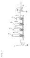
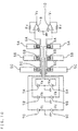
- FIG. 1 is a plan view that shows one example of a sensor main body in a vibration wave detector of the present invention.
- the sensor main body 1 formed on a semiconductor silicon substrate 20, is constituted by a diaphragm 2 for receiving an inputted sound wave, a transversal beam 3 that is connected to the diaphragm 2, a terminator 4 connected to the tip of the transversal beam 3, and a plurality (n number) of resonator beams 5 each of which has one end supported by the transversal beam 3, and all of these parts are made of semiconductor silicon.
- each resonator beam 5 is a resonator the length of which is adjusted so as to resonate at a specific frequency.
- the resonant frequency f of each resonator beam 5 is set at a desired value by changing its thickness a or its length X; thus, each resonator beam 5 has an inherent resonant frequency.
- the thickness a of all the resonator beams 5 is constant, and the length X thereof is successively increased from the right side (the diaphragm 2 side) toward the left side (the terminator 4 side); therefore, the resonant frequency at which each resonant beam 5 inherently vibrates is high at the right side (the diaphragm 2 side) and is gradually reduced toward the left side (the terminator 4 side).
- Table 1 shows one example of specific specifications of the sensor main body 1 including n number of resonator beams 5.
- the thicknesses of the diaphragm 2, the transversal beam 3 and the terminator 4 are the same as the thickness (a) of the resonator beam 5.
- Parameter Value Number of resonator beams 5 (n) 29 Thickness (a) 10 ⁇ m Length of resonator beam 5 (X i ) 2450r i-29 ⁇ m Width of resonator beam 5 (b) 80 ⁇ m Pitch of resonator beam 5 (d) 120 ⁇ m Width of transversal beam 3 (Z i ) 60r 29-i ⁇ m r 2 1/48 ⁇ 1.0145
- the sensor main body 1 having the above-mentioned arrangement is formed on the semiconductor silicon substrate 20 by using a micromachining technique.
- the diaphragm 2 is allowed to vibrate, and the vibrating wave representing the sound wave is transmitted to the transversal beam 3, and further transferred to the terminator 4 with the resonator beams 5, each of which has one end supported by the transversal beam 3, being successively allowed to resonate at their specific frequencies.
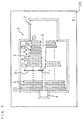
- FIG. 2 shows a circuit diagram that shows a vibration wave detector of the present invention in which such a sensor main body 1 is used.
- These plural piezoresistors 6 are connected in parallel with one another, and one end of the parallel circuit is connected to a DC power supply 7 (voltage V 0 ), and the other end thereof is connected to the minus input terminal of an operational amplifier 8.
- the operational amplifier 8 has its plus input terminal connected to ground.
- the DC power supply 7 commonly applies a bias voltage V 0 to all the resonant beams 5.
- V 0 bias voltage
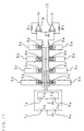
- FIG. 3 is a plan view that shows another example of the sensor main body 1 in the vibration wave detector of the present invention.
- a plurality of resonator beams 5, the length of which is adjusted so as to resonate in response to a specific frequency, are placed only on one side of the transversal beam 3
- n number of pairs of the resonator beams 5 having the same resonant frequency are placed on both sides of the transversal beam 3.
- each pair of the resonator beams 5, 5, which are connected to the same position of the transversal beam 3 in the length direction have the same length and the same resonant frequency.
- the other members such as the diaphragm 2, the transversal beam 3 and the terminator 4 have the same arrangement as those of the first embodiment.
- the actual specifications are also the same as those of the embodiment 1 (Table 1). That is, in the same manner as the embodiment 1, the thickness a of all the resonator beams 5 is constant, and the length X thereof is successively lengthened from the right side (the diaphragm 2 side) toward the left side (the terminator 4 side), with the result that the diaphragm 2 side forms a high-frequency side in the resonant frequency.
- FIG. 4 is a circuit diagram that shows a vibration wave detector of the present invention in which such a sensor main body 1 is used.
- the same members as those of FIG. 2 are indicated by the same reference numerals.
- pairs of the resonator beams 5, 5, each pair having the same resonant frequency are provided (that is, the fishbone structure); therefore, two pairs of parallel circuits to which the piezoresistors 6 are connected are provided, DC power supplies 7 and 9 for applying DC bias voltages V 0 and - V 0 to the respective parallel circuits are provided, and operational amplifiers 8 and 10 for getting output signals from the respective parallel circuits are provided.
- twice as much output is obtained by adding the output signals from the two parallel circuits.
- the arrangement shown in FIG. 4 makes it possible to provide an output signal having a corresponding frequency component by using the other resonator beam 5 paired by the resonator beam 5 having the abnormality, and consequently to prevent the detection error.
- the reasons that the piezoresistors 6 are used as a method for converting a mechanical vibration into an electric signal are because they are easily manufactured, because they have a linear conversion characteristic and because they have a high conversion efficiency.
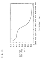
- FIG. 5 is a graph that shows the results of an FEM analysis in which the amplitude at the tip of each resonator beam 5 is simulated when a sound wave of 0.1 Pa is inputted to the diaphragm 2.
- the resonator beams 5 in the graph are successively numbered from the diaphragm 2 side. As can be seen from the graph, it is confirmed that the sensor main body 1 of the present invention has a superior frequency selectivity.
- each resonator beam 5 When such a resonance occurs in each resonator beam 5, the resistance value of the piezoresistor 6 formed in each resonator beam 5 is changed due to the strain.
- a constant bias voltage V 0 is applied to the respective parallel-connected piezoresistors 6 so that the changes in the resistance value of the piezoresistors 6, caused by the strain in each resonator beam 5, are added as electric currents flowing through one signal line.
- the output voltage V + of the operational amplifier 8 is represented by the following equation (3).
- the second term represents a variant voltage caused by a vibration.
- equations (5) and (6) show that the contribution ratio and the variant voltage can be controlled independently by the shape (W i /L i ) of the piezoresistor 6 in each resonator beam 5, and can also be controlled in a constant manner by the bias voltage V 0 with respect to all the resonator beams 5.
- the gain of the variant voltage is dependent on the shape of the piezoresistor 6, it is possible to adjust the output gain for each of the resonator beams 5 by changing the shape of the piezoresistor 6 formed in the resonator beam 5, that is, by changing the resistance value of the piezoresistor 6.
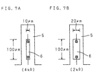
- the width W i of the rectangular piezoresistor 6 it is possible to change the resistance value from 4 k ⁇ to 2 k ⁇ .
- FIGS. 8A through 8D are drawings that show another example of the change in the resistance value.
- a slit 21 (FIG. 8B) is formed in a direction orthogonal to the direction of strain by using, for example, laser trimming, in one portion of the rectangular piezoresistor 6 (FIG. 8A) formed in each resonator beam 5.
- FIG. 8C shows an equivalent electric circuit prior to the formation of the slit 21, and
- FIG. 8D shows an equivalent electric circuit after the formation of the slit 21.
- the resistance R' at the bottleneck portion formed by the slit 21 is apparently connected in series with the resistance R + ⁇ R so that the resistance value as a whole is changed.
- the value of resistance R' can be adjusted by the length of the slit 21, and since the slit width is so small that the value of resistance R + ⁇ R is regarded as constant independent of the formation of the slit 21, it is possible to control the output gain of the resonator beam 5 by using the value of resistance R', that is, depending on how the slit 21 is formed.
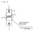
- FIG. 9 is a drawing that shows still another example of the change in the resistance value.
- two slits 21, 21 are formed so that the direction of a current flowing through the bottleneck portion is made orthogonal to the direction of strain.
- the bottleneck portion through which the current flows in the direction orthogonal to the direction of strain has no change in its specific resistivity due to the strain.
- the bottleneck portion, which forms an additional resistor can be changed in both its length and width depending on how the slits 21, 21 are formed; therefore, it becomes possible to provide a greater degree of freedom in adjusting the value of resistance R' as compared with the aforementioned example.
- the width of the bottleneck portion forms a parameter of the value of resistance R', and the width needs to be extremely narrowed so as to increase the value, resulting in a greater limitation to the machining process.
- the length and width of the bottleneck portion form the parameters of the value of resistance R', it is possible to widen the control range of the output gain in the resonator beam 5.
- the slit 21 as shown in FIG. 8B and FIG. 9 may be formed by using a photolithography technique during the manufacturing process of the sensor, or may be formed by using laser trimming or focused ion-beam irradiation after the manufacturing process of the sensor. In either case, the gain adjustment can be carried out by applying laser trimming or focused ion-beam irradiation to the manufactured sensor.
- the contribution ratio and the variant voltage are controlled by a bias voltage V 0 to be applied to the piezoresistor 6 of each resonator beam 5 based upon equations (5) and (6).
- V 0 bias voltage
- the gain of the variant voltage is dependent on the bias voltage V 0 to the piezoresistor 6, the output gain can be adjusted for each resonator beam 5 by changing the bias voltage V 0 .
- FIG. 10 is a circuit diagram that shows one example of a vibration wave detector of the present invention in which the bias voltage to the piezoresistor 6 in each resonator beam 5 is changed.
- the same members as those of FIG. 4 are indicated by the same reference numerals.
- one end of the piezoresistor 6 of each resonator beam 5 is connected to an independent power supply so that a bias voltage having a different magnitude is applied to each of the piezoresistors 6.
- piezoresistors 6A, 6B and 6C formed in three resonator beams 5A, 5B and 5C respectively, have their one end connected to respectively independent DC power supplies 7A, 7B and 7C (9A, 9B and 9C), and have their other end formed into a common output terminal; thus, different bias voltages V A (-V A ), V B (-V B ) and V C (-V C ) are applied to the respective piezoresistors 6A, 6B and 6C.
- the magnitudes of the bias voltages to be applied to the respective piezoresistors 6A, 6B and 6C are determined in accordance with gains that are desirably set in the respective resonator beams 5A, 5B and 5C.
- FIG. 11 is a circuit diagram that shows still another example of a vibration wave detector in which a bias voltage to the piezoresistor 6 in each resonator beam 5 is changed.
- the same members as those of FIG. 4 are indicated by the same reference numerals.
- all the resonator beams 5 are divided into a plurality of blocks, each having a specific frequency band that is to be set at the same desired gain, and in each block, the piezoresistors 6 in the respective resonator beams 5 are connected in parallel with one another, and one end of each parallel circuit is connected to an independent power supply corresponding to the desired gain to be set so that bias voltages having the same magnitude are applied to the piezoresistors 6 included in the same block.
- four resonator beams 5 are divided into two blocks, that is, one block on the high resonant frequency side including two resonator beams 5a and 5b and another block on the low resonant frequency side including two resonator beams 5c and 5d. Then, in the respective two blocks, the piezoresistors 6a and 6b are connected and the piezoresistors 6c and 6d are connected.
- each parallel circuit is connected to respectively independent DC power supplies 7a and 7c (9a and 9c), and the other ends are formed into a common output terminal,
- a bias voltage V a (-V a ) is applied from the DC power supply 7a (9a) to the piezoresistors 6a and 6b on the high frequency side
- a bias voltage V c (-V c ) is applied from the DC power supply 7c (9c) to the piezoresistors 6c and 6d on the low frequency side.
- the magnitudes of the bias voltages V a (-V a ) and V c (-V c ) to be applied to the respective parallel circuits are determined for each block (for each frequency band) in accordance with the desired gain to be set.
- a sensor main body 1 having a transversal beam 3 on both sides of which two pairs of the resonator beams 5, each pair having 29 resonator beams, are formed the resonator beams 5 of the two pairs, each consisting of 25 resonator beams S except the respective two located at the ends, are divided into 8 blocks for each of predetermined frequency bands. As shown in FIG.
- a bias voltage of 5 V is applied to the four blocks on the low-frequency side (the resonator beams 5 from the 27th to 16th: the resonant frequency of the 16th resonator beam 5 is 3400 Hz), and a bias voltage of 0 V is applied to the four blocks (the resonator beams 5 from the 3 rd to 15th) on the high-frequency side.
- FIG. 13 shows the results of a simulation carried out on the frequency and the amplitude of the variant voltage in this state.
- the magnitude of the variant voltage decreases with 3400 Hz being a turning point; this confirms that a frequency response applicable as an LPF (Low-Pass Filter) has been achieved.
- LPF Low-Pass Filter
- a bias voltage that varies with time may be applied to the vibration sensors of the first and second embodiments.
- an AC voltage is used as the bias voltage, it becomes possible to obtain a signal in which the amplitude of the vibration is modulated.
- FIG. 14 is a perspective view that shows the third embodiment of the vibration wave detector of the present invention.
- the arrangement of the sensor main body 1 shown in FIG. 14 is substantially the same as that of the first embodiment; therefore, the same members are indicated by the same reference numerals and the description thereof is omitted.
- Electrodes 11 are formed on the semiconductor silicon substrate 20 at positions facing the tips of the respective resonator beams 5 so that a capacitor is formed by the tip of each resonator beam 5 and each electrode 11 facing it.
- the tip of each resonator beam 5 is a movable electrode the position of which is raised and lowered in response to the vibration, while the electrode 11, formed on the semiconductor silicon substrate 20 is a fixed electrode the position of which is not allowed to move.
- the resonator beam 5 vibrates at a specific frequency, the distance between the two electrodes varies, with the result that the capacity of the capacitor is changed.
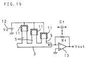
- FIG. 15 is a circuit diagram that explains the third embodiment.
- a plurality of electrodes 11 are connected in parallel with one another, and one end of the parallel circuit is connected to a DC power supply 12 (voltage V 0 ).
- the transversal beam 3 is connected to the minus input terminal of an operational amplifier 13.
- the plus input terminal of the operational amplifier 13 is connected to ground.
- the voltage V 0 is commonly applied to all the electrodes 11 by the DC power supply 12.
- resonance of the respective resonator beams 5 is outputted as the sum of variations.
- resonance of the respective resonator beams 5 is outputted as the sum of velocities.
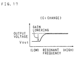
- FIG. 16 is a plan view that shows an example in which the capacitor C i is changed, and the area of an electrode 11C that corresponds to the longest resonator beam 5C among the three resonator beams 5A, 5B and 5C is made smaller than the area of each of electrodes 11A and 11B that relate to the other two resonator beams 5A and 5B.
- FIG. 17 shows the relationship between the resonant frequency and the output voltage V out , in the above-mentioned case.
- the gain in the low-frequency area can be selectively made lower than the gains in the other frequency areas.
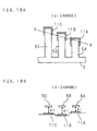
- FIG. 18A is a plan view that shows an example in which the distance d i is changed
- FIG. 18B is a cross-sectional view taken along line X-X of FIG. 18A.
- the distance between the shortest resonator beam 5A among the three resonator beams 5A, 5B and 5C and the corresponding electrode 11A is made shortest, and the distance between the resonator beam 5B having an intermediate length and the corresponding electrode 11B is made longest.
- FIG. 19 shows the relationship between the resonant frequency and the output voltage V out in the above-mentioned case.
- the gain in the high-frequency area can be made highest, and the gain in the intermediate-frequency area can be made lowest.
- FIG. 20 is a plan view that shows an example in which the minute change ⁇ d i of the distance is changed.
- electrodes 11A and 11B corresponding to the two of the resonator beams 5A and 5B among the three resonator beams 5A, 5B and 5C are formed so as to face the tips of the resonator beams 5A and 5B, while an electrode 11C corresponding to the longest resonator beam 5C is formed so as to face the base end of the resonator beam 5C.
- FIG. 21 shows the relationship between the resonant frequency and the output voltage V out in the above-mentioned case.
- a bias voltage that varies with time to the vibration sensors of the third embodiment.
- an AC voltage is used as the bias voltage, it is possible to obtain a signal in which the amplitude of vibration is modulated.
- the arrangement in which n number of pairs of the resonator beams 5, each pair having the same resonant frequency, are formed on both sides of the transversal beam 3 may of course be adopted, with the same effect that the gain adjustment of each resonator beam 5 can be carried out by changing the capacitor C i , the distance d i and the minute change ⁇ d i in the distance.
- the gain of the electric output is controlled by making the conditions (the area, shape, installation position, etc.) of the detector (the piezoresistors 6 and the electrodes 11) variable; however, these conditions may be respectively set for each resonator beam 5 at the time of installing the detector during the manufacturing process of the vibration wave detector, or the condition setting may be changed after the detector has been installed.
- a plurality of resonators having respectively different resonant frequencies are formed into an array, and in response to an inputted vibration wave, each resonator is allowed to respond selectively with its resonant frequency so that upon detecting the intensity of each frequency component of the vibration wave, the detection gain in each resonator can be adjusted; thus, it becomes possible to realize a vibration wave sensor by which a desired frequency characteristic is obtained.
Applications Claiming Priority (4)
| Application Number | Priority Date | Filing Date | Title |
|---|---|---|---|
| JP14191598 | 1998-05-22 | ||
| JP14191598 | 1998-05-22 | ||
| JP12530399 | 1999-04-30 | ||
| JP12530399A JP3348686B2 (ja) | 1998-05-22 | 1999-04-30 | 振動波検出方法及び装置 |
Publications (3)
| Publication Number | Publication Date |
|---|---|
| EP0959333A2 true EP0959333A2 (fr) | 1999-11-24 |
| EP0959333A3 EP0959333A3 (fr) | 2003-01-15 |
| EP0959333B1 EP0959333B1 (fr) | 2008-01-02 |
Family
ID=26461771
Family Applications (1)
| Application Number | Title | Priority Date | Filing Date |
|---|---|---|---|
| EP99110076A Expired - Lifetime EP0959333B1 (fr) | 1998-05-22 | 1999-05-22 | Méthode et dispositif por détecter des ondes de vibrations |
Country Status (8)
| Country | Link |
|---|---|
| US (1) | US6079274A (fr) |
| EP (1) | EP0959333B1 (fr) |
| JP (1) | JP3348686B2 (fr) |
| KR (1) | KR100354976B1 (fr) |
| AU (1) | AU746037B2 (fr) |
| DE (1) | DE69937858T2 (fr) |
| DK (1) | DK0959333T3 (fr) |
| TW (1) | TWI243238B (fr) |
Cited By (6)
| Publication number | Priority date | Publication date | Assignee | Title |
|---|---|---|---|---|
| DE10129456A1 (de) * | 2001-06-19 | 2003-01-09 | Fraunhofer Ges Forschung | Vorrichtung und Verfahren zur Erfassung und Analyse von Schallsignalen |
| WO2006105528A1 (fr) * | 2005-03-31 | 2006-10-05 | Intel Corporation | Reseau de capteurs de spectre de vibrations micro-usines ultrasensibles en silicium (vssa) |
| US7600429B2 (en) | 2006-04-20 | 2009-10-13 | Intel Corporation | Vibration spectrum sensor array having differing sensors |
| EP2442445A1 (fr) * | 2010-10-12 | 2012-04-18 | Nxp B.V. | Oscillateur MEMS |
| EP2986024A1 (fr) * | 2014-08-13 | 2016-02-17 | Samsung Electronics Co., Ltd | Dispositif de détection audio et procédé d'acquisition d'informations de fréquence |
| EP3972128A1 (fr) * | 2020-09-17 | 2022-03-23 | Samsung Electronics Co., Ltd. | Interface de capteur comprenant un résonateur et un amplificateur différentiel |
Families Citing this family (18)
| Publication number | Priority date | Publication date | Assignee | Title |
|---|---|---|---|---|
| JP3348687B2 (ja) * | 1998-05-22 | 2002-11-20 | 住友金属工業株式会社 | 振動波検出方法及び装置 |
| US6360611B1 (en) * | 2000-04-21 | 2002-03-26 | Kohji Toda | Device for ultrasound radiation into a material |
| US6600389B2 (en) * | 2001-05-30 | 2003-07-29 | Intel Corporation | Tapered structures for generating a set of resonators with systematic resonant frequencies |
| KR20050059075A (ko) * | 2002-08-20 | 2005-06-17 | 더 리전트 오브 더 유니버시티 오브 캘리포니아 | 진동 검출기, 음 검출기, 보청기, 와우각 이식물 및 이와관련된 방법 |
| KR100583103B1 (ko) | 2002-12-31 | 2006-05-23 | 주식회사 하이닉스반도체 | 반도체 소자의 제조 방법 |
| US7088031B2 (en) * | 2003-04-22 | 2006-08-08 | Infinite Power Solutions, Inc. | Method and apparatus for an ambient energy battery or capacitor recharge system |
| US20080178682A1 (en) * | 2005-01-10 | 2008-07-31 | The Regents Of The University Of California | Resonator circuit having reduced effects of parasitic feed-through capacitance |
| JP2006200976A (ja) * | 2005-01-19 | 2006-08-03 | Denso Corp | 超音波センサ |
| JP4539920B2 (ja) * | 2006-05-12 | 2010-09-08 | 国立大学法人 東京大学 | 振動波検出方法及び装置 |
| JP2008008683A (ja) * | 2006-06-27 | 2008-01-17 | Univ Of Tokyo | 振動波検出方法及び装置 |
| JP2008139136A (ja) * | 2006-12-01 | 2008-06-19 | Matsushita Electric Ind Co Ltd | 力学量センサおよびその製造方法 |
| KR100999838B1 (ko) | 2008-05-09 | 2010-12-09 | 한국과학기술원 | 다중외팔보 mems 센서의 제조방법 및 다중외팔보 mems 센서를 이용한 음원위치 추정방법 |
| US9105751B2 (en) | 2011-11-11 | 2015-08-11 | International Business Machines Corporation | Integrated semiconductor devices with single crystalline beam, methods of manufacture and design structure |
| US8546240B2 (en) | 2011-11-11 | 2013-10-01 | International Business Machines Corporation | Methods of manufacturing integrated semiconductor devices with single crystalline beam |
| US8629036B2 (en) | 2011-11-11 | 2014-01-14 | International Business Machines Corporation | Integrated semiconductor devices with amorphous silicon beam, methods of manufacture and design structure |
| KR102454950B1 (ko) * | 2015-12-11 | 2022-10-14 | 삼성전자주식회사 | 분광기 및 분광기를 포함하는 이미지 센서 |
| JP7030331B2 (ja) * | 2018-03-28 | 2022-03-07 | リバーエレテック株式会社 | Aeセンサ素子及びaeセンサ |
| KR20200059379A (ko) * | 2018-11-20 | 2020-05-29 | 삼성전자주식회사 | 공진기, 이를 포함하는 공진기 시스템 및 공진기 제조 방법 |
Citations (2)
| Publication number | Priority date | Publication date | Assignee | Title |
|---|---|---|---|---|
| US4885781A (en) * | 1987-09-17 | 1989-12-05 | Messerschmitt-Bolkow-Blohm Gmbh | Frequency-selective sound transducer |
| US5001933A (en) * | 1989-12-26 | 1991-03-26 | The United States Of America As Represented By The Secretary Of The Army | Micromechanical vibration sensor |
Family Cites Families (2)
| Publication number | Priority date | Publication date | Assignee | Title |
|---|---|---|---|---|
| US3614678A (en) * | 1967-08-11 | 1971-10-19 | Gen Electric | Electromechanical filters with integral piezoresistive output and methods of making same |
| US5856722A (en) * | 1996-01-02 | 1999-01-05 | Cornell Research Foundation, Inc. | Microelectromechanics-based frequency signature sensor |
-
1999
- 1999-04-30 JP JP12530399A patent/JP3348686B2/ja not_active Expired - Fee Related
- 1999-05-20 TW TW089107773A patent/TWI243238B/zh not_active IP Right Cessation
- 1999-05-21 AU AU31218/99A patent/AU746037B2/en not_active Ceased
- 1999-05-21 US US09/316,586 patent/US6079274A/en not_active Expired - Fee Related
- 1999-05-21 KR KR1019990018516A patent/KR100354976B1/ko not_active IP Right Cessation
- 1999-05-22 DE DE69937858T patent/DE69937858T2/de not_active Expired - Lifetime
- 1999-05-22 EP EP99110076A patent/EP0959333B1/fr not_active Expired - Lifetime
- 1999-05-22 DK DK99110076T patent/DK0959333T3/da active
Patent Citations (2)
| Publication number | Priority date | Publication date | Assignee | Title |
|---|---|---|---|---|
| US4885781A (en) * | 1987-09-17 | 1989-12-05 | Messerschmitt-Bolkow-Blohm Gmbh | Frequency-selective sound transducer |
| US5001933A (en) * | 1989-12-26 | 1991-03-26 | The United States Of America As Represented By The Secretary Of The Army | Micromechanical vibration sensor |
Non-Patent Citations (1)
| Title |
|---|
| "DISCRETE FOURIER TRANSFORM USING CAPACITIVE CANTILEAVERS" IBM TECHNICAL DISCLOSURE BULLETIN, IBM CORP. NEW YORK, US, vol. 40, no. 10, 1 October 1997 (1997-10-01), pages 53-55, XP000739420 ISSN: 0018-8689 * |
Cited By (12)
| Publication number | Priority date | Publication date | Assignee | Title |
|---|---|---|---|---|
| DE10129456A1 (de) * | 2001-06-19 | 2003-01-09 | Fraunhofer Ges Forschung | Vorrichtung und Verfahren zur Erfassung und Analyse von Schallsignalen |
| WO2006105528A1 (fr) * | 2005-03-31 | 2006-10-05 | Intel Corporation | Reseau de capteurs de spectre de vibrations micro-usines ultrasensibles en silicium (vssa) |
| US7559242B2 (en) | 2005-03-31 | 2009-07-14 | Intel Corporation | Silicon micromachined ultra-sensitive vibration spectrum sensor array (VSSA) |
| US7600429B2 (en) | 2006-04-20 | 2009-10-13 | Intel Corporation | Vibration spectrum sensor array having differing sensors |
| EP2442445A1 (fr) * | 2010-10-12 | 2012-04-18 | Nxp B.V. | Oscillateur MEMS |
| US8564377B2 (en) | 2010-10-12 | 2013-10-22 | Nxp B.V. | MEMS oscillator |
| EP2986024A1 (fr) * | 2014-08-13 | 2016-02-17 | Samsung Electronics Co., Ltd | Dispositif de détection audio et procédé d'acquisition d'informations de fréquence |
| KR20160020287A (ko) * | 2014-08-13 | 2016-02-23 | 삼성전자주식회사 | 음향 센싱 소자 및 주파수 정보 획득 방법 |
| US9479884B2 (en) | 2014-08-13 | 2016-10-25 | Samsung Electronics Co., Ltd. | Audio sensing device and method of acquiring frequency information |
| US10225662B2 (en) | 2014-08-13 | 2019-03-05 | Samsung Electronics Co., Ltd. | Audio sensing device and method of acquiring frequency information |
| EP3972128A1 (fr) * | 2020-09-17 | 2022-03-23 | Samsung Electronics Co., Ltd. | Interface de capteur comprenant un résonateur et un amplificateur différentiel |
| US11770658B2 (en) | 2020-09-17 | 2023-09-26 | Samsung Electronics Co., Ltd. | Sensor interface including resonator and differential amplifier |
Also Published As
| Publication number | Publication date |
|---|---|
| DK0959333T3 (da) | 2008-05-13 |
| AU746037B2 (en) | 2002-04-11 |
| KR100354976B1 (ko) | 2002-10-05 |
| US6079274A (en) | 2000-06-27 |
| DE69937858D1 (de) | 2008-02-14 |
| EP0959333B1 (fr) | 2008-01-02 |
| KR19990088491A (ko) | 1999-12-27 |
| AU3121899A (en) | 1999-12-02 |
| JP2000046639A (ja) | 2000-02-18 |
| DE69937858T2 (de) | 2009-01-02 |
| TWI243238B (en) | 2005-11-11 |
| EP0959333A3 (fr) | 2003-01-15 |
| JP3348686B2 (ja) | 2002-11-20 |
Similar Documents
| Publication | Publication Date | Title |
|---|---|---|
| EP0959333A2 (fr) | Méthode et dispositif por détecter des ondes de vibrations | |
| US6223601B1 (en) | Vibration wave detecting method and vibration wave detector | |
| US4940914A (en) | Vibration absorbing apparatus | |
| US20030127944A1 (en) | Tunable piezoelectric micro-mechanical resonator | |
| US5113698A (en) | Vibrating beam transducer drive system | |
| JPH053536B2 (fr) | ||
| US6281618B1 (en) | Vibrating gyroscope | |
| US6810737B2 (en) | Resonant element and vibration adjusting method therefor | |
| JP3353728B2 (ja) | 音響振動センサ | |
| Scheibner et al. | Characterization and self-test of electrostatically tunable resonators for frequency selective vibration measurements | |
| US5606214A (en) | Smart actuator for active surface control | |
| JP3230347B2 (ja) | 角速度センサ | |
| JP2000205940A (ja) | センサ素子及び振動波センサ | |
| US6012341A (en) | Force sensor having an adjustable distance between an operating point and a point of mechanical instability | |
| US11770658B2 (en) | Sensor interface including resonator and differential amplifier | |
| US8614609B2 (en) | Resonant filter based on an N/MEMS matrix | |
| US20220326188A1 (en) | Multi frequency acoustic emission micromachined transducers for non-destructive evaluation of structural health | |
| JPH06249873A (ja) | 加速度センサ | |
| Chen et al. | Vibration signature analysis sensors for predictive diagnostics | |
| Suzuki et al. | An optical diffraction microphone with active grating diaphragm | |
| JPH01312425A (ja) | 力学量センサ | |
| JPH0526130B2 (fr) | ||
| JPH01107161A (ja) | 振動加速度センサ |
Legal Events
| Date | Code | Title | Description |
|---|---|---|---|
| PUAI | Public reference made under article 153(3) epc to a published international application that has entered the european phase |
Free format text: ORIGINAL CODE: 0009012 |
|
| AK | Designated contracting states |
Kind code of ref document: A2 Designated state(s): AT BE CH CY DE DK ES FI FR GB GR IE IT LI LU MC NL PT SE |
|
| AX | Request for extension of the european patent |
Free format text: AL;LT;LV;MK;RO;SI |
|
| PUAL | Search report despatched |
Free format text: ORIGINAL CODE: 0009013 |
|
| AK | Designated contracting states |
Kind code of ref document: A3 Designated state(s): AT BE CH CY DE DK ES FI FR GB GR IE IT LI LU MC NL PT SE |
|
| AX | Request for extension of the european patent |
Free format text: AL;LT;LV;MK;RO;SI |
|
| 17P | Request for examination filed |
Effective date: 20030220 |
|
| AKX | Designation fees paid |
Designated state(s): CH DE DK FR GB IT LI NL |
|
| RAP1 | Party data changed (applicant data changed or rights of an application transferred) |
Owner name: TOKYO ELECTRON LIMITED |
|
| 17Q | First examination report despatched |
Effective date: 20041221 |
|
| GRAP | Despatch of communication of intention to grant a patent |
Free format text: ORIGINAL CODE: EPIDOSNIGR1 |
|
| GRAS | Grant fee paid |
Free format text: ORIGINAL CODE: EPIDOSNIGR3 |
|
| GRAA | (expected) grant |
Free format text: ORIGINAL CODE: 0009210 |
|
| AK | Designated contracting states |
Kind code of ref document: B1 Designated state(s): CH DE DK FR GB IT LI NL |
|
| REG | Reference to a national code |
Ref country code: GB Ref legal event code: FG4D |
|
| REG | Reference to a national code |
Ref country code: CH Ref legal event code: EP |
|
| REF | Corresponds to: |
Ref document number: 69937858 Country of ref document: DE Date of ref document: 20080214 Kind code of ref document: P |
|
| REG | Reference to a national code |
Ref country code: CH Ref legal event code: NV Representative=s name: ISLER & PEDRAZZINI AG |
|
| REG | Reference to a national code |
Ref country code: DK Ref legal event code: T3 |
|
| ET | Fr: translation filed | ||
| PLBE | No opposition filed within time limit |
Free format text: ORIGINAL CODE: 0009261 |
|
| STAA | Information on the status of an ep patent application or granted ep patent |
Free format text: STATUS: NO OPPOSITION FILED WITHIN TIME LIMIT |
|
| 26N | No opposition filed |
Effective date: 20081003 |
|
| PGFP | Annual fee paid to national office [announced via postgrant information from national office to epo] |
Ref country code: IT Payment date: 20100522 Year of fee payment: 12 |
|
| PG25 | Lapsed in a contracting state [announced via postgrant information from national office to epo] |
Ref country code: IT Free format text: LAPSE BECAUSE OF NON-PAYMENT OF DUE FEES Effective date: 20110522 |
|
| PGFP | Annual fee paid to national office [announced via postgrant information from national office to epo] |
Ref country code: NL Payment date: 20120523 Year of fee payment: 14 Ref country code: DK Payment date: 20120510 Year of fee payment: 14 Ref country code: DE Payment date: 20120516 Year of fee payment: 14 Ref country code: CH Payment date: 20120514 Year of fee payment: 14 |
|
| PGFP | Annual fee paid to national office [announced via postgrant information from national office to epo] |
Ref country code: GB Payment date: 20120516 Year of fee payment: 14 Ref country code: FR Payment date: 20120608 Year of fee payment: 14 |
|
| REG | Reference to a national code |
Ref country code: NL Ref legal event code: V1 Effective date: 20131201 |
|
| REG | Reference to a national code |
Ref country code: CH Ref legal event code: PL |
|
| GBPC | Gb: european patent ceased through non-payment of renewal fee |
Effective date: 20130522 |
|
| PG25 | Lapsed in a contracting state [announced via postgrant information from national office to epo] |
Ref country code: CH Free format text: LAPSE BECAUSE OF NON-PAYMENT OF DUE FEES Effective date: 20130531 Ref country code: LI Free format text: LAPSE BECAUSE OF NON-PAYMENT OF DUE FEES Effective date: 20130531 Ref country code: DE Free format text: LAPSE BECAUSE OF NON-PAYMENT OF DUE FEES Effective date: 20131203 |
|
| REG | Reference to a national code |
Ref country code: DK Ref legal event code: EBP Effective date: 20130531 |
|
| REG | Reference to a national code |
Ref country code: DE Ref legal event code: R119 Ref document number: 69937858 Country of ref document: DE Effective date: 20131203 |
|
| PG25 | Lapsed in a contracting state [announced via postgrant information from national office to epo] |
Ref country code: NL Free format text: LAPSE BECAUSE OF NON-PAYMENT OF DUE FEES Effective date: 20131201 |
|
| REG | Reference to a national code |
Ref country code: FR Ref legal event code: ST Effective date: 20140131 |
|
| PG25 | Lapsed in a contracting state [announced via postgrant information from national office to epo] |
Ref country code: DK Free format text: LAPSE BECAUSE OF NON-PAYMENT OF DUE FEES Effective date: 20130531 Ref country code: GB Free format text: LAPSE BECAUSE OF NON-PAYMENT OF DUE FEES Effective date: 20130522 |
|
| PG25 | Lapsed in a contracting state [announced via postgrant information from national office to epo] |
Ref country code: FR Free format text: LAPSE BECAUSE OF NON-PAYMENT OF DUE FEES Effective date: 20130531 |