EP0951145B1 - Schaltung zur Erfassung von analogen binären Signalen - Google Patents
Schaltung zur Erfassung von analogen binären Signalen Download PDFInfo
- Publication number
- EP0951145B1 EP0951145B1 EP99400879A EP99400879A EP0951145B1 EP 0951145 B1 EP0951145 B1 EP 0951145B1 EP 99400879 A EP99400879 A EP 99400879A EP 99400879 A EP99400879 A EP 99400879A EP 0951145 B1 EP0951145 B1 EP 0951145B1
- Authority
- EP
- European Patent Office
- Prior art keywords
- circuit
- input
- schmitt
- logic
- output
- Prior art date
- Legal status (The legal status is an assumption and is not a legal conclusion. Google has not performed a legal analysis and makes no representation as to the accuracy of the status listed.)
- Expired - Lifetime
Links
- 238000012360 testing method Methods 0.000 claims description 14
- 238000001514 detection method Methods 0.000 claims description 8
- 238000013475 authorization Methods 0.000 claims description 6
- 230000000295 complement effect Effects 0.000 claims 1
- 235000021183 entrée Nutrition 0.000 description 29
- 238000010586 diagram Methods 0.000 description 11
- 230000006978 adaptation Effects 0.000 description 4
- 238000005516 engineering process Methods 0.000 description 4
- 238000001914 filtration Methods 0.000 description 4
- 230000010354 integration Effects 0.000 description 3
- 238000000034 method Methods 0.000 description 3
- 230000035945 sensitivity Effects 0.000 description 3
- 238000012512 characterization method Methods 0.000 description 2
- 230000000694 effects Effects 0.000 description 2
- 230000005764 inhibitory process Effects 0.000 description 2
- 230000003044 adaptive effect Effects 0.000 description 1
- 230000003042 antagnostic effect Effects 0.000 description 1
- 230000009194 climbing Effects 0.000 description 1
- 230000003247 decreasing effect Effects 0.000 description 1
- 231100001261 hazardous Toxicity 0.000 description 1
- 238000004519 manufacturing process Methods 0.000 description 1
- 238000012986 modification Methods 0.000 description 1
- 230000004048 modification Effects 0.000 description 1
- 230000002093 peripheral effect Effects 0.000 description 1
- 230000000750 progressive effect Effects 0.000 description 1
- 230000000630 rising effect Effects 0.000 description 1
- 230000001052 transient effect Effects 0.000 description 1
- 230000007704 transition Effects 0.000 description 1
Images


Classifications
-
- G—PHYSICS
- G11—INFORMATION STORAGE
- G11C—STATIC STORES
- G11C27/00—Electric analogue stores, e.g. for storing instantaneous values
- G11C27/02—Sample-and-hold arrangements
- G11C27/024—Sample-and-hold arrangements using a capacitive memory element
-
- H—ELECTRICITY
- H03—ELECTRONIC CIRCUITRY
- H03K—PULSE TECHNIQUE
- H03K3/00—Circuits for generating electric pulses; Monostable, bistable or multistable circuits
- H03K3/02—Generators characterised by the type of circuit or by the means used for producing pulses
- H03K3/027—Generators characterised by the type of circuit or by the means used for producing pulses by the use of logic circuits, with internal or external positive feedback
- H03K3/037—Bistable circuits
- H03K3/0377—Bistables with hysteresis, e.g. Schmitt trigger
-
- H—ELECTRICITY
- H03—ELECTRONIC CIRCUITRY
- H03K—PULSE TECHNIQUE
- H03K5/00—Manipulating of pulses not covered by one of the other main groups of this subclass
- H03K5/01—Shaping pulses
- H03K5/08—Shaping pulses by limiting; by thresholding; by slicing, i.e. combined limiting and thresholding
-
- H—ELECTRICITY
- H03—ELECTRONIC CIRCUITRY
- H03K—PULSE TECHNIQUE
- H03K5/00—Manipulating of pulses not covered by one of the other main groups of this subclass
- H03K5/125—Discriminating pulses
- H03K5/1252—Suppression or limitation of noise or interference
Definitions
- the present invention as defined in the claims relates to the acquisition of signals binary analog at the input of a digital integrated circuit.
- Schmitt triggers which present a tilt hysteresis with two distinct thresholds: a high threshold at the climb and a low threshold on the descent.
- the Schmitt trigger input digital stage is realized in a cell of the digital integrated circuit.
- it has the disadvantage of having its electrical characteristics, therefore its thresholds of tilting, frozen during the characterization of its integration cell.
- cell characterization is an expensive operation that we try to avoid as much as possible. It is as is usual to define the architecture of an integrated circuit digital ASIC (Application Specific Integrated Circuit in language Anglo-Saxon) prediffused or precharacterized, from a combination of precharacterized cells of various types, established in advance and grouped together in library.
- ASIC Application Specific Integrated Circuit in language Anglo-Saxon
- the designer of an ASIC circuit has therefore, to discretize a binary analog signal, that a choice among a game reduced by several types of digital trigger input stages Schmitt with fixed characteristics, game often limited to two types, one TTL standard, the other CMOS standard. It sometimes happens that among the set of Schmitt trigger input digital stages none are really suitable so unless you do develop a specific cell, which is expensive, the designer of a ASIC circuit must opt for an available type of input stage Schmitt trigger digital with high tilt thresholds and that are not the ones you want but just theirs relatives. The digital integrated circuit obtained then manifests a more high sensitivity to noise or requires a more adaptive stage complex.
- the object of the present invention is to combat this disadvantage by increasing, for an integrated circuit designer digital ASIC, the possibilities of choice of threshold levels of up and down of an input digital stage despite the limitation imposed by a reduced number of digital stage types input to Schmitt trigger precharacterized in library.
- Its object is a circuit for the acquisition of a signal binary analog with multiple Schmitt triggers as input with different tilt thresholds, connected in parallel by their inputs, and followed by at least one logic discretization circuit deducing the state of the binary analog signal from the combination of states output of input Schmitt triggers.
- the discretization logic circuit comprises feedback means allowing a temporary forcing of the level signal input from Schmitt triggers.
- the discretization logic circuit can be used to increase or decrease the apparent hysteresis of two Schmitt triggers having stepped high and low tilt thresholds.
- it When used to increase the apparent hysteresis, it includes a logical rocker changing state on the one hand, during the transition to logical level 1 of the Schmitt trigger having the highest high tilt threshold and on the other hand when switching to logic level 0 of the Schmitt trigger having the lowest tipping threshold.
- Schmitt trigger When used for decrease the apparent hysteresis of two Schmitt triggers having stepped high and low tilt thresholds, it includes a toggle logic changing state on the one hand, when passing to logic level 0 of the Schmitt trigger having the highest low tilt threshold and, on the other hand, when switching to logic level 1 of the Schmitt trigger having the lowest high tilting threshold and means for feedback forcing the Schmitt trigger to a high threshold for a short time highest tilting when crossing its high threshold dice crossing up the upper threshold of the other Schmitt trigger by the input signal, and the Schmitt trigger at the low threshold of lowest tipping when crossing its low threshold as soon as crossing down from the low threshold of the other Schmitt trigger by the input signal.
- the discretization logic circuit by allowing select one of the input Schmitt triggers for crossing at the rise of its high threshold and another for crossing at the lowering of its low threshold while ensuring, when it turns out necessary, a feedback guaranteeing the sensitivity of these two Schmitt triggers at the crossings of these two thresholds does more than double the freedom of choice of the digital integrated circuit designer ASIC, this freedom of choice being all the greater as the number of types of input Schmitt trigger is high.
- the circuit for the acquisition of a signal binary analog is part of a digital integrated circuit in a case and has its various input Schmitt triggers connected as an input to a same connection pin of the digital integrated circuit box.
- the digital integrated circuit in a housing contains several copies of circuit for signal acquisition binary analog each having their different Schmitt triggers input connected to the same pin of the circuit box integrated digital and individual test means of each of the thresholds triggers based on logical door chains of the "no and" type each connected at the outputs of the same type of Schmitt triggers.
- the circuit for the acquisition of a signal binary analog includes, in addition to Schmitt triggers with different switching thresholds, connected in parallel by their inputs, and of the discretization logic circuit which is connected to the outputs of the Schmitt triggers and which deduces the state of the analog signal binary of the combination of the exit states of the Schmitt triggers, a digital output filter eliminating transient noise caused by the asynchronous operations of the various Schmitt triggers.
- the circuit for the acquisition of a signal binary analog includes, in addition to Schmitt triggers with different switching thresholds, connected in parallel by their inputs, and of the discretization logic circuit which is connected to the outputs of the Schmitt triggers and which deduces the state of the analog signal binary of the combination of the exit states of the Schmitt triggers, failure detection means detecting prohibited combinations between the output states of the various Schmitt triggers.
- the circuit for the acquisition of a signal binary analog includes, in addition to Schmitt triggers with different switching thresholds, connected in parallel by their inputs, and of the discretization logic circuit which is connected to the outputs of the Schmitt triggers and which deduces the state of the analog signal binary of the combination of the exit states of the Schmitt triggers, failure detection means detecting prohibited combinations between the output states of the various Schmitt triggers and triggering only when prohibited combinations between states of exit of the various Schmitt triggers beyond a certain duration.
- the circuit for the acquisition of a signal binary analog has several discretization logic circuits different and a circuit for selecting the output of one of your choice discretization logic circuits.
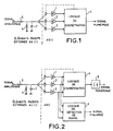
- the circuit for the acquisition of a binary analog signal which will be described, is integrated on the chip of an ASIC digital circuit. It is represented in FIG. 1 behind a purely passive analog stage, outside the ASIC digital integrated circuit chip, bringing the range voltage variation of the binary analog signal across the voltage variation range allowed by the digital integrated circuit ASIC. It essentially comprises, an entrance floor consisting of a bank of Schmitt triggers 1, 2, 3 of different types including inputs are connected in parallel, and an output stage consisting of a circuit discretization logic 4 deducing the state of the binary analog signal of the combination of the output states of the Schmitt trigger bank input 1, 2, 3 and possibly acting on the input signal (dotted feedback connection) to raise awareness of triggers Schmitt.
- the passive analog input stage which is outside the circuit integrated digital ASIC, is constituted, in the usual way by a voltage divider bridge with two resistors 5, 6 supplemented by a filtering capacity 7. It serves, as indicated above, to adapt the voltage variation range of the binary analog signal, which is often several tens of volts, at the voltage variation range allowed by the integrated circuit ASIC, which is generally between 0 and 5 volts and sometimes less.
- the Schmitt trigger bank 1, 2, 3 placed at the entrance to the the actual circuit for acquiring a binary analog signal is made up of at least two different types of Schmitt triggers including the cells in the ASIC digital integrated circuit were precharacterized and are part of a cell library at the layout of the integrated circuit designer. These two types are by example the CMOS type with a hysteresis value of around 1.9 volts between the high and low trigger thresholds of a trigger, and the TTL type with a hysteresis value of approximately 0.6 volts between the thresholds of up and down switching of a trigger. Of course, there can be other types of Schmitt trigger with different values hysteresis. It suffices for this that these other types have been precharacterized and appear in the cell library available from the ASIC designer.
- the discretization logic circuit 4 is a logic circuit combinatorial and / or sequential, possibly even of memory type, which deduces the state of the binary analog signal from the combination of states output of the different Schmitt triggers 1, 2, 3. It can be, as shown in Figure 2 followed by a digital noise filter 8 and doubled by a fault detection circuit 9.
- the digital noise filter eliminates transients due to asynchronous operations of the different triggers by Schmitt.
- the filtering capacity 7 of the passive analog stage input then acts as an anti-aliasing filter necessary for good operation of this digital noise filter.
- the fault detection circuit 9 is a logic circuit combinatorial and / or sequential, possibly even of memory type, which locates the prohibited combinations of the output states of the triggers of Schmitt 1, 2, 3 for fault detection purposes. It emits a signal alarm when it finds that a prohibited combination between the output states of the various Schmitt triggers beyond one certain duration.
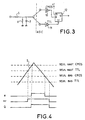
- FIG. 3 illustrates a practical embodiment of a circuit for the acquisition of a binary analog signal in the frequent case, where the cell library available to the circuit designer integrated ASIC contains only two types of Schmitt trigger, one at CMOS standard, the other TTL standard and where you want to increase hysteresis.
- the input Schmitt trigger bank consists of a CMOS 10 Schmitt trigger and a Schmitt trigger to TTL 11 standard and the logic circuit discretization by a storage register 12 active on level.
- the storage register 12 has a given input D carried to the level logic + 1, a registration authorization input e connected to the output of the CMOS standard Schmitt 10 trigger, an additional input priority reset nr connected at the output of the Schmitt trigger 11 to TTL standard and a given Q output.
- the Q output of the storage 12 goes to logic level 1 each time the signal binary analog input crosses the high standard threshold on the rise CMOS and logic level 0 whenever the analog signal entry crosses the lower threshold of the TTL standard when descending.
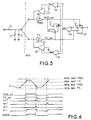
- the digital circuits of output 27, 28 impose their output level + 1 or 0 on the inputs of the Schmitt triggers 20, 21 due to non-zero output impedance of the analog input stage used for range scaling variation of the binary analog input signal.
- the first storage circuit 22 of the logic circuit of discretization which delivers the output signal on its data output Q, goes to logic level 1 each time the Schmitt trigger 21 at standard TTL switches to high state and logic level 0 each time that the CMOS standard Schmitt 20 trigger switches to the low state.
- the two Schmitt triggers 20, 21 must be CMOS and TTL standards are sensitive to passing one of its threshold low when the high threshold of the other has been crossed, the other of its high threshold when the other's low threshold has been crossed, which implies that they have previously seen the binary analog input signal crossing their other threshold in the opposite direction.
- the first logic gate 24 detects the instants during which the binary analog input signal has crossed by increasing the TTL high threshold but has not yet crossed the CMOS high threshold, or crossed below the low CMOS threshold but did not cross the threshold low TTL. Its output signal "sa1" thus identifies the instants or a forcing may be necessary so as to make it later one of the triggers sensitive to the crossing of its antagonistic threshold.
- the second storage register 23 identifies that of the Schmitt triggers 20, 21 which is likely to be forced. If its release of data Q is at logic level 0, is that the amplitude of the signal binary analog input went below the TTL low threshold without be passed again above the high CMOS threshold and the threshold at force is possibly the high CMOS threshold. If its data output Q is at logic level 1, is that the amplitude of the analog signal input binary passed above the high CMOS threshold without being again passed below the low TTL threshold and the threshold to be forced is possibly the low TTL threshold.
- the second logic gate 25 combines a logic level 0 in output of the second storage register 23 and a logic level 1 at the output of the first logic gate 24 to cause a forcing temporary amplitude of the binary analog input signal beyond from the high trigger switch threshold to the CMOS standard.
- the third logic gate 26 combines a logic level 1 in output of the second storage register 23 and a logic level 1 at the output of the first logic gate 24 to cause a forcing temporary amplitude of the binary analog input signal in below the low threshold for triggering the TTL standard trigger.
- the diagrams in Figure 6 illustrate the shape of the different signals found at different points in the diagram in Figure 5 for a binary analog input signal S 'evolving between the high threshold CMOS switching threshold and TTL low switching threshold, without achieve so far.
- the CMOS_out curve illustrates the shape of the signal in output of the CMOS standard Schmitt 20 trigger taking into account effects of forcing circuits.
- the TTL_out curve illustrates the shape of the signal at the output of the Schmitt 21 trigger in TTL standard taking into account effects of forcing circuits.
- the curve sa1 illustrates the shape of the output signal of the first logic gate 24. We notice that it goes to logic level 1 each time a forcing in one direction or in the other may be necessary.
- the curve sa2 illustrates the shape of the second logic gate 25 output signal. goes to logic level 1 each time a signal forcing analog binary input beyond the high CMOS switchover threshold may be necessary.
- the curve sa3 illustrates the shape of the signal output of the third logic gate 26. We notice that it goes to the logic level 1 whenever a binary analog signal is forced entry below the low TTL tilt threshold may be necessary.
- the curve sl1 illustrates the shape of the signal on the output of data Q of the second storage register 23 and the OUTPUT curve the form of the signal at the output of the discretization logic circuit.
- first storage register 22 could be replaced by a logic gate of type "or".
- the precise constitution of the circuit discretization logic depends on the result we are looking for, that is to say of the two combinations of Schmitt trigger output states of the input stage which one wishes to associate with the two states of the signal binary analog. It is even possible, when the signal analog binary input can be exchanged, provide a choice between several different selections of high and low thresholds by connecting several different discretization logic circuits in parallel on the outputs of the input trigger bank and having a selector circuit at the outputs of the different discretization logic circuits.
- FIG 7 there is shown very schematically the chip of an integrated circuit 30 on its housing 31 to illustrate the wire connections between connection pins 32 of the box 31 and the connection pads 33, 34 or "pads" of the chip 30.
- the inputs of Schmitt's triggers are in parallel so it's possible to connect their connection pads 33, 34 to the same pin 32, which limits the number of pins connection of the integrated circuit box.
- the technique of logical door chains of type "no and” called technique of "nand tree” in Anglo-Saxon language.
- Figure 8 illustrates the implementation of the technique of "nand tree" in the case of an ASIC digital integrated circuit containing three circuits for the acquisition of a binary analog signal 40, respectively 41 and 42 of the same type as that of FIG. 3, having each the inputs of their two Schmitt triggers wired to a same connection terminal 400, respectively 401 and 402 of the housing of the ASIC digital integrated circuit.
- the chain for testing CMOS-type Schmitt triggers presents a first logic gate 50 of type "no and” to two inputs with one input raised to logic level + 1 and the other connected to a specific connection terminal 500 on the circuit box integrated ASIC via a Schmitt trigger.
- first logic gate 50 there comes a second logic gate 51 type "no and” with two inputs, with one input connected to the output of the first logic gate 50 and an input connected to the output of the CMOS-type Schmitt trigger of a first acquisition circuit 40.
- the chain for testing TTL type Schmitt triggers has a similar structure with different "non” type logic gates and "with two inputs 60, 61, 62, 63, and two connection terminals individual on the case of the integrated circuit ASIC, one 600 for its entry and the other 601 for its exit.
Landscapes
- Physics & Mathematics (AREA)
- Nonlinear Science (AREA)
- Manipulation Of Pulses (AREA)
Claims (12)
- Schaltung zur Erfassung eines analogen binären Signals, dadurch gekennzeichnet, daß es am Eingang mindestens zwei Schmitt-Trigger (10, 11) mit hohen und niedrigen gestuften Schaltschwellen umfaßt, die mit ihren Eingängen parallel geschaltet und am Ausgang von mindestens einer Diskretisierungslogikschaltung (4) gefolgt sind, die einerseits beim Übergang zum Logikpegel 1 des Schmitt-Triggers (10) mit der höheren hohen Schaltschwelle und andererseits beim Übergang zum Logikpegel 0 des Schmitt-Triggers (11) mit der niedrigeren niedrigen Schaltschwelle den Zustand ändert.
- Schaltung nach Anspruch 1, dadurch gekennzeichnet, daß die Diskretisierungslogikschaltung (4) ein Logikgatter des Typs "UND" ist.
- Schaltung nach Anspruch 1, dadurch gekennzeichnet, daß die Diskretisierungslogikschaltung (4) ein Speicherregister (12) mit einem auf den Logikpegel +1 gesetzten Dateneingang D, einem mit dem Ausgang eines (10) der Schmitt-Trigger verbundenen Schreibberechtigungseingang e und einem mit dem Ausgang des anderen (11) der Schmitt-Trigger verbundenen komplementierten Nullstellungseingang nr ist.
- Schaltung zur Erfassung eines analogen binären Signals, dadurch gekennzeichnet, daß es am Eingang mindestens zwei Schmitt-Trigger (20, 21) mit hohen und niedrigen gestuften Schaltschwellen umfaßt, die mit ihren Eingängen parallel geschaltet und am Ausgang von mindestens einer Diskretisierungslogikschaltung (4) gefolgt sind, die einerseits beim Übergang zum Logikpegel 0 des Schmitt-Triggers (20) mit der höheren niedrigen Schaltschwelle und andererseits beim Übergang zum Logikpegel 1 des Schmitt-Triggers (21) mit der niedrigeren hohen Schaltschwelle den Zustand ändert, und Rückkopplungsmittel (23, 24, 25, 26, 27, 28), die kurzzeitig den Schmitt-Trigger (20) mit der höheren hohen Schaltschwelle bei Überschreitung seiner hohen Schwelle nach der Überschreitung der hohen Schaltschwelle des anderen Schmitt-Triggers (21) durch das Eingangssignal bei seinem Anstieg und den Schmitt-Trigger (21) mit der niedrigeren niedrigen Schaltschwelle bei Überschreitung seiner niedrigen Schwelle nach der Überschreitung der niedrigen Schaltschwelle des anderen Schmitt-Triggers (20) durch das Eingangssignal bei seinem Abstieg setzt.
- Schaltung nach Anspruch 4, dadurch gekennzeichnet, daß die Diskretisierungslogikschaltung (4) ein Logikgatter des Typs "ODER" ist.
- Schaltung nach Anspruch 4, dadurch gekennzeichnet, daß die Diskretisierungslogikschaltung (4) ein Speicherregister (22) mit einem auf den Logikpegel +1 gesetzten Dateneingang D, einem mit dem Ausgang eines (21) der Schmitt-Trigger verbundenen Schreibberechtigungseingang e und einem mit dem Ausgang des anderen (20) der Schmitt-Trigger verbundenen komplementierten Nullstellungseingang nr ist.
- Schaltung nach Anspruch 1 oder Anspruch 4, die Teil einer integrierten Schaltung in einem Gehäuse ist, dadurch gekennzeichnet, daß ihre unterschiedlichen Eingangs-Schmitt-Trigger am Eingang mit einem gleichen Verbindungsstift des Gehäuses der digitalen integrierten Schaltung verbunden sind.
- Schaltung nach Anspruch 1 oder Anspruch 4, deren mehrere Exemplare Teil einer gleichen integrierten Schaltung im Gehäuse bilden, dadurch gekennzeichnet, daß die integrierte Schaltung im Gehäuse mit Mitteln zum Einzeltest jedes der Schwellen der Schmitt-Trigger der verschiedenen Exemplare der Schaltung ausgerüstet ist, wobei die Testmittel hauptsächlich Ketten von Logikgattern des Typs "NICHT-UND" sind, die jeweils mit dem Ausgang eines selben Typs von Schmitt-Triggern verbunden sind.
- Schaltung nach Anspruch 1 oder Anspruch 4, dadurch gekennzeichnet, daß sie auch ein mit dem Ausgang der Diskretisierungslogikschaltung (4) verbundenes digitales Rauschfilter (8) umfaßt.
- Schaltung nach Anspruch 1 oder Anspruch 4, dadurch gekennzeichnet, daß sie auch eine Störungserkennungslogikschaltung (9) umfaßt, die am Eingang parallel zu der Diskretisierungslogikschaltung (4) geschaltet ist und die verbotene Kombinationen zwischen Ausgangszuständen der verschiedenen Eingangs-Schmitt-Trigger (1, 2, 3) erkennt.
- Schaltung nach Anspruch 10, dadurch gekennzeichnet, daß die Störungserkennungslogikschaltung (9) ein Alarmsignal erzeugt, wenn verbotene Kombinationen zwischen Ausgangszuständen der verschiedenen Eingangs-Schmitt-Trigger (1, 2, 3) über eine gewisse Dauer hinaus anhalten.
- Schaltung nach Anspruch 1 oder Anspruch 4, dadurch gekennzeichnet, daß sie mehrere unterschiedliche Diskretisierungslogikschaltungen (4) umfaßt, die parallel mit den Ausgängen der Eingangs-Schmitt-Trigger (1, 2, 3) verbunden sind und von einer Auswahlschaltung des Ausgangssignals von einer unter ihnen gefolgt sind.
Applications Claiming Priority (2)
| Application Number | Priority Date | Filing Date | Title |
|---|---|---|---|
| FR9804859 | 1998-04-17 | ||
| FR9804859A FR2777717B1 (fr) | 1998-04-17 | 1998-04-17 | Circuit pour l'acquisition de signaux analogiques binaires |
Publications (2)
| Publication Number | Publication Date |
|---|---|
| EP0951145A1 EP0951145A1 (de) | 1999-10-20 |
| EP0951145B1 true EP0951145B1 (de) | 2004-03-03 |
Family
ID=9525386
Family Applications (1)
| Application Number | Title | Priority Date | Filing Date |
|---|---|---|---|
| EP99400879A Expired - Lifetime EP0951145B1 (de) | 1998-04-17 | 1999-04-09 | Schaltung zur Erfassung von analogen binären Signalen |
Country Status (5)
| Country | Link |
|---|---|
| US (1) | US6204786B1 (de) |
| EP (1) | EP0951145B1 (de) |
| CA (1) | CA2267535A1 (de) |
| DE (1) | DE69915155D1 (de) |
| FR (1) | FR2777717B1 (de) |
Families Citing this family (22)
| Publication number | Priority date | Publication date | Assignee | Title |
|---|---|---|---|---|
| FR2822319B1 (fr) * | 2001-03-16 | 2003-05-30 | Thomson Csf | Commutateur de trames d'informations de taille variable pour reseaux securitaires embarques |
| DE10135798B4 (de) * | 2001-07-23 | 2008-10-16 | Robert Bosch Gmbh | Verfahren und Vorrichtung zur Diagnose diskreter Endstufen über Digitaleingänge |
| FR2828046B1 (fr) * | 2001-07-27 | 2003-10-10 | Thales Sa | Procede de gestion de taches pour un automate de routage d'un commutateur de paquets faisant partie d'un reseau securise de transmission a commutation par paquets |
| US6805225B2 (en) * | 2002-04-08 | 2004-10-19 | Roberta Freedman | Combination travel and laundry bag |
| FR2840482B1 (fr) * | 2002-05-28 | 2004-10-15 | Thales Sa | Procede de reconstitution de messages achemines par un ou plusieurs reseaux de transmission par paquets |
| JP3809585B2 (ja) * | 2004-02-10 | 2006-08-16 | 日本テキサス・インスツルメンツ株式会社 | ヒステリシス型入力回路 |
| FR2900749B1 (fr) * | 2006-05-05 | 2008-07-25 | Thales Sa | Procede et dispositif de securisation de la memoire d'un calculateur a l'encontre des erreurs dues aux radiations |
| FR2933829B1 (fr) * | 2008-07-08 | 2015-08-07 | Thales Sa | Dispositif et procede de detection de l'origine numerique d'un signal analogique |
| FR2977045B1 (fr) * | 2011-06-23 | 2015-12-11 | Thales Sa | Dispositif de memoire corrigeant l'effet de collisions de particules a hautes energie. |
| US8901955B2 (en) * | 2012-11-05 | 2014-12-02 | Sandisk Technologies Inc. | High speed buffer with high noise immunity |
| ITTO20130307A1 (it) | 2013-04-17 | 2014-10-18 | Itt Italia Srl | Metodo per realizzare un elemento frenante, in particolare una pastiglia freno, sensorizzato, pastiglia freno sensorizzata, impianto frenante di veicolo e metodo associato |
| TWI498572B (zh) * | 2013-05-07 | 2015-09-01 | Wistron Corp | 自動測量dvb-s接收裝置的調諧器的輸出電壓的方法、轉接器及dvb-s接收裝置 |
| US9939035B2 (en) | 2015-05-28 | 2018-04-10 | Itt Italia S.R.L. | Smart braking devices, systems, and methods |
| ITUB20151184A1 (it) * | 2015-05-28 | 2016-11-28 | Itt Italia Srl | Condizionatore del segnale elettrico proveniente da almeno un sensore piezoceramico di un dispositivo frenante per veicoli |
| MX387883B (es) * | 2015-05-28 | 2025-03-19 | Itt Italia Srl | Dispositivo de frenado para vehiculos que comprende un acondicionador para acondicionar la señal electrica procedente de al menos un sensor piezoceramico del dispositivo de frenado. |
| ITUB20153709A1 (it) | 2015-09-17 | 2017-03-17 | Itt Italia Srl | Dispositivo di analisi e gestione dei dati generati da un sistema frenante sensorizzato per veicoli |
| ITUB20153706A1 (it) | 2015-09-17 | 2017-03-17 | Itt Italia Srl | Dispositivo frenante per veicolo pesante e metodo di prevenzione del surriscaldamento dei freni in un veicolo pesante |
| ITUA20161336A1 (it) | 2016-03-03 | 2017-09-03 | Itt Italia Srl | Dispositivo e metodo per il miglioramento delle prestazioni di un sistema antibloccaggio e antiscivolamento di un veicolo |
| IT201600077944A1 (it) | 2016-07-25 | 2018-01-25 | Itt Italia Srl | Dispositivo per il rilevamento della coppia residua di frenatura in un veicolo equipaggiato con freni a disco |
| CN109445347A (zh) * | 2018-11-16 | 2019-03-08 | 美钻深海能源科技研发(上海)有限公司 | 一种现场采集信号的数字显示单元及其显示方法 |
| IT201900015839A1 (it) | 2019-09-06 | 2021-03-06 | Itt Italia Srl | Pastiglia freno per veicoli e suo processo di produzione |
| WO2022248114A1 (en) | 2021-05-25 | 2022-12-01 | Itt Italia S.R.L. | A method and a device for estimating residual torque between the braked and braking elements of a vehicle |
Family Cites Families (8)
| Publication number | Priority date | Publication date | Assignee | Title |
|---|---|---|---|---|
| JPS5461863A (en) * | 1977-10-27 | 1979-05-18 | Fujitsu Ltd | Waveform shaping circuit |
| US4418332A (en) * | 1981-06-24 | 1983-11-29 | Harris Corporation | Noise insensitive comparator |
| JP2693198B2 (ja) * | 1988-06-16 | 1997-12-24 | ローベルト ボツシユ ゲゼルシヤフト ミツト ベシユレンクテル ハフツング | 伝送線の上のスイツチの状態検出装置 |
| DE3837821A1 (de) * | 1988-11-08 | 1990-05-10 | Asea Brown Boveri | Cmos-praezisions-schmitt-trigger |
| DE4141547A1 (de) * | 1991-12-17 | 1993-06-24 | Bosch Gmbh Robert | Schaltungsanordnung zur erzeugung einer drehzahlabhaengigen signalfolge |
| US5341046A (en) * | 1992-12-07 | 1994-08-23 | Ncr Corporation | Threshold controlled input circuit for an integrated circuit |
| US5563532A (en) * | 1994-01-24 | 1996-10-08 | Advanced Micro Devices, Inc. | Double filtering glitch eater for elimination of noise from signals on a SCSI bus |
| JP3527814B2 (ja) * | 1996-10-03 | 2004-05-17 | 沖電気工業株式会社 | 集積回路 |
-
1998
- 1998-04-17 FR FR9804859A patent/FR2777717B1/fr not_active Expired - Fee Related
-
1999
- 1999-04-09 EP EP99400879A patent/EP0951145B1/de not_active Expired - Lifetime
- 1999-04-09 DE DE69915155T patent/DE69915155D1/de not_active Expired - Lifetime
- 1999-04-14 US US09/291,044 patent/US6204786B1/en not_active Expired - Fee Related
- 1999-04-15 CA CA002267535A patent/CA2267535A1/fr not_active Abandoned
Also Published As
| Publication number | Publication date |
|---|---|
| FR2777717A1 (fr) | 1999-10-22 |
| CA2267535A1 (fr) | 1999-10-17 |
| DE69915155D1 (de) | 2004-04-08 |
| EP0951145A1 (de) | 1999-10-20 |
| FR2777717B1 (fr) | 2002-12-06 |
| US6204786B1 (en) | 2001-03-20 |
Similar Documents
| Publication | Publication Date | Title |
|---|---|---|
| EP0951145B1 (de) | Schaltung zur Erfassung von analogen binären Signalen | |
| US11302591B2 (en) | Scan testable through silicon VIAs | |
| KR101027170B1 (ko) | 차동 감지 방식을 이용하여 저 전압으로 프로그램 가능한eFUSE | |
| EP0080394A1 (de) | Bistabile Kippschaltung mit energieunabhängiger Haltbarkeit und statischer Rücksetzung | |
| EP0318363A1 (de) | Verfahren zum Testen von Zellen von elektrisch programmierbaren Speichern und entsprechende integrierte Schaltung | |
| FR2681180A1 (fr) | Circuit de regulation de tension de programmation, pour memoires programmables. | |
| FR2728689A1 (fr) | Circuit d'etalonnage de resistances | |
| EP2779221A1 (de) | Verfahren, Vorrichtung und automatisches Erkennungssystem von Störungen in TSV-Durchgangslöchern | |
| EP0459863B1 (de) | Integrierter Schaltkreis mit Anschlussstift zur Modusfeststellung | |
| EP3623827B1 (de) | Elektronischer chip mit analogen eingängen/ausgängen mit selbsttestmitteln | |
| EP0080395A1 (de) | Bistabile Kippschaltung mit energieunabhängiger Haltbarkeit und dynamischer Rücksetzung | |
| EP0972207B1 (de) | Verbindungstestverfahren | |
| FR3112004A1 (fr) | Détection d'une impulsion électromagnétique | |
| US20100105155A1 (en) | Digital trimming in a microelectronic device | |
| EP1560032B1 (de) | Verfahren zur Absicherung des Testmodus einer integrierten Schaltung mittels Eindringungserkennung | |
| EP0424222A1 (de) | Integrierte Logikschaltung mit einstellbaren Àbergangszeiten | |
| EP1688753B1 (de) | Sicherung des Testmodus eines integrierten Schaltkreises | |
| FR2676844A1 (fr) | Dispositif de memoire a semiconducteurs avec redondance. | |
| EP2069814B1 (de) | Parametrisches scan-register, digitale schaltung und verfahren zum prüfen einer digitalen schaltung unter verwendung eines solchen registers | |
| EP3614156A1 (de) | Elektronischer schaltkreis | |
| EP1877811A1 (de) | Integrierte schaltung mit einem sicheren prüfmodus, der integrierte-schaltungs-konfigurierbare zellenkettenstatusdetektion verwendet | |
| FR2773652A1 (fr) | Circuit de generation d'un signal d'activation commande | |
| FR2793088A1 (fr) | Procede et dispositif de collecte des valeurs logiques de sortie d'une unite logique dans un circuit electronique | |
| FR2888330A1 (fr) | Circuit integre comportant un mode de test securise par detection de l'etat d'un signal de commande | |
| FR2666902A1 (fr) | Circuit integre avec registre de test peripherique. |
Legal Events
| Date | Code | Title | Description |
|---|---|---|---|
| PUAI | Public reference made under article 153(3) epc to a published international application that has entered the european phase |
Free format text: ORIGINAL CODE: 0009012 |
|
| AK | Designated contracting states |
Kind code of ref document: A1 Designated state(s): DE FR GB IT |
|
| AX | Request for extension of the european patent |
Free format text: AL;LT;LV;MK;RO;SI |
|
| RAP1 | Party data changed (applicant data changed or rights of an application transferred) |
Owner name: THOMSON-CSF SEXTANT |
|
| 17P | Request for examination filed |
Effective date: 20000126 |
|
| AKX | Designation fees paid |
Free format text: DE FR GB IT |
|
| RAP1 | Party data changed (applicant data changed or rights of an application transferred) |
Owner name: THALES AVIONICS S.A. |
|
| GRAP | Despatch of communication of intention to grant a patent |
Free format text: ORIGINAL CODE: EPIDOSNIGR1 |
|
| GRAS | Grant fee paid |
Free format text: ORIGINAL CODE: EPIDOSNIGR3 |
|
| GRAA | (expected) grant |
Free format text: ORIGINAL CODE: 0009210 |
|
| AK | Designated contracting states |
Kind code of ref document: B1 Designated state(s): DE FR GB IT |
|
| PG25 | Lapsed in a contracting state [announced via postgrant information from national office to epo] |
Ref country code: IT Free format text: LAPSE BECAUSE OF FAILURE TO SUBMIT A TRANSLATION OF THE DESCRIPTION OR TO PAY THE FEE WITHIN THE PRESCRIBED TIME-LIMIT;WARNING: LAPSES OF ITALIAN PATENTS WITH EFFECTIVE DATE BEFORE 2007 MAY HAVE OCCURRED AT ANY TIME BEFORE 2007. THE CORRECT EFFECTIVE DATE MAY BE DIFFERENT FROM THE ONE RECORDED. Effective date: 20040303 Ref country code: GB Free format text: LAPSE BECAUSE OF FAILURE TO SUBMIT A TRANSLATION OF THE DESCRIPTION OR TO PAY THE FEE WITHIN THE PRESCRIBED TIME-LIMIT Effective date: 20040303 |
|
| REG | Reference to a national code |
Ref country code: GB Ref legal event code: FG4D Free format text: NOT ENGLISH |
|
| PGFP | Annual fee paid to national office [announced via postgrant information from national office to epo] |
Ref country code: FR Payment date: 20040408 Year of fee payment: 6 |
|
| REF | Corresponds to: |
Ref document number: 69915155 Country of ref document: DE Date of ref document: 20040408 Kind code of ref document: P |
|
| PG25 | Lapsed in a contracting state [announced via postgrant information from national office to epo] |
Ref country code: DE Free format text: LAPSE BECAUSE OF FAILURE TO SUBMIT A TRANSLATION OF THE DESCRIPTION OR TO PAY THE FEE WITHIN THE PRESCRIBED TIME-LIMIT Effective date: 20040604 |
|
| GBV | Gb: ep patent (uk) treated as always having been void in accordance with gb section 77(7)/1977 [no translation filed] |
Effective date: 20040303 |
|
| PLBE | No opposition filed within time limit |
Free format text: ORIGINAL CODE: 0009261 |
|
| STAA | Information on the status of an ep patent application or granted ep patent |
Free format text: STATUS: NO OPPOSITION FILED WITHIN TIME LIMIT |
|
| 26N | No opposition filed |
Effective date: 20041206 |
|
| PG25 | Lapsed in a contracting state [announced via postgrant information from national office to epo] |
Ref country code: FR Free format text: LAPSE BECAUSE OF NON-PAYMENT OF DUE FEES Effective date: 20051230 |
|
| REG | Reference to a national code |
Ref country code: FR Ref legal event code: ST Effective date: 20051230 |