EP0949837B1 - ATM Koppelfeld - Google Patents
ATM Koppelfeld Download PDFInfo
- Publication number
- EP0949837B1 EP0949837B1 EP99301545A EP99301545A EP0949837B1 EP 0949837 B1 EP0949837 B1 EP 0949837B1 EP 99301545 A EP99301545 A EP 99301545A EP 99301545 A EP99301545 A EP 99301545A EP 0949837 B1 EP0949837 B1 EP 0949837B1
- Authority
- EP
- European Patent Office
- Prior art keywords
- wavelength
- atm switch
- cell
- signal
- cells
- Prior art date
- Legal status (The legal status is an assumption and is not a legal conclusion. Google has not performed a legal analysis and makes no representation as to the accuracy of the status listed.)
- Expired - Lifetime
Links
Images


Classifications
-
- H—ELECTRICITY
- H04—ELECTRIC COMMUNICATION TECHNIQUE
- H04L—TRANSMISSION OF DIGITAL INFORMATION, e.g. TELEGRAPHIC COMMUNICATION
- H04L12/00—Data switching networks
- H04L12/54—Store-and-forward switching systems
- H04L12/56—Packet switching systems
- H04L12/5601—Transfer mode dependent, e.g. ATM
-
- H—ELECTRICITY
- H04—ELECTRIC COMMUNICATION TECHNIQUE
- H04B—TRANSMISSION
- H04B10/00—Transmission systems employing electromagnetic waves other than radio-waves, e.g. infrared, visible or ultraviolet light, or employing corpuscular radiation, e.g. quantum communication
- H04B10/80—Optical aspects relating to the use of optical transmission for specific applications, not provided for in groups H04B10/03 - H04B10/70, e.g. optical power feeding or optical transmission through water
- H04B10/801—Optical aspects relating to the use of optical transmission for specific applications, not provided for in groups H04B10/03 - H04B10/70, e.g. optical power feeding or optical transmission through water using optical interconnects, e.g. light coupled isolators, circuit board interconnections
-
- H—ELECTRICITY
- H04—ELECTRIC COMMUNICATION TECHNIQUE
- H04L—TRANSMISSION OF DIGITAL INFORMATION, e.g. TELEGRAPHIC COMMUNICATION
- H04L49/00—Packet switching elements
- H04L49/15—Interconnection of switching modules
- H04L49/1553—Interconnection of ATM switching modules, e.g. ATM switching fabrics
-
- H—ELECTRICITY
- H04—ELECTRIC COMMUNICATION TECHNIQUE
- H04L—TRANSMISSION OF DIGITAL INFORMATION, e.g. TELEGRAPHIC COMMUNICATION
- H04L49/00—Packet switching elements
- H04L49/30—Peripheral units, e.g. input or output ports
- H04L49/3081—ATM peripheral units, e.g. policing, insertion or extraction
-
- H—ELECTRICITY
- H04—ELECTRIC COMMUNICATION TECHNIQUE
- H04L—TRANSMISSION OF DIGITAL INFORMATION, e.g. TELEGRAPHIC COMMUNICATION
- H04L49/00—Packet switching elements
- H04L49/45—Arrangements for providing or supporting expansion
- H04L49/455—Provisions for supporting expansion in ATM switches
-
- H—ELECTRICITY
- H04—ELECTRIC COMMUNICATION TECHNIQUE
- H04Q—SELECTING
- H04Q11/00—Selecting arrangements for multiplex systems
- H04Q11/0001—Selecting arrangements for multiplex systems using optical switching
- H04Q11/0005—Switch and router aspects
-
- H—ELECTRICITY
- H04—ELECTRIC COMMUNICATION TECHNIQUE
- H04L—TRANSMISSION OF DIGITAL INFORMATION, e.g. TELEGRAPHIC COMMUNICATION
- H04L12/00—Data switching networks
- H04L12/54—Store-and-forward switching systems
- H04L12/56—Packet switching systems
- H04L12/5601—Transfer mode dependent, e.g. ATM
- H04L2012/5603—Access techniques
- H04L2012/5604—Medium of transmission, e.g. fibre, cable, radio
- H04L2012/5605—Fibre
-
- H—ELECTRICITY
- H04—ELECTRIC COMMUNICATION TECHNIQUE
- H04L—TRANSMISSION OF DIGITAL INFORMATION, e.g. TELEGRAPHIC COMMUNICATION
- H04L12/00—Data switching networks
- H04L12/54—Store-and-forward switching systems
- H04L12/56—Packet switching systems
- H04L12/5601—Transfer mode dependent, e.g. ATM
- H04L2012/5672—Multiplexing, e.g. coding, scrambling
-
- H—ELECTRICITY
- H04—ELECTRIC COMMUNICATION TECHNIQUE
- H04L—TRANSMISSION OF DIGITAL INFORMATION, e.g. TELEGRAPHIC COMMUNICATION
- H04L12/00—Data switching networks
- H04L12/54—Store-and-forward switching systems
- H04L12/56—Packet switching systems
- H04L12/5601—Transfer mode dependent, e.g. ATM
- H04L2012/5678—Traffic aspects, e.g. arbitration, load balancing, smoothing, buffer management
- H04L2012/5681—Buffer or queue management
-
- H—ELECTRICITY
- H04—ELECTRIC COMMUNICATION TECHNIQUE
- H04Q—SELECTING
- H04Q11/00—Selecting arrangements for multiplex systems
- H04Q11/0001—Selecting arrangements for multiplex systems using optical switching
- H04Q11/0005—Switch and router aspects
- H04Q2011/0007—Construction
- H04Q2011/0016—Construction using wavelength multiplexing or demultiplexing
-
- H—ELECTRICITY
- H04—ELECTRIC COMMUNICATION TECHNIQUE
- H04Q—SELECTING
- H04Q11/00—Selecting arrangements for multiplex systems
- H04Q11/0001—Selecting arrangements for multiplex systems using optical switching
- H04Q11/0005—Switch and router aspects
- H04Q2011/0052—Interconnection of switches
-
- H—ELECTRICITY
- H04—ELECTRIC COMMUNICATION TECHNIQUE
- H04Q—SELECTING
- H04Q11/00—Selecting arrangements for multiplex systems
- H04Q11/0001—Selecting arrangements for multiplex systems using optical switching
- H04Q11/0005—Switch and router aspects
- H04Q2011/0052—Interconnection of switches
- H04Q2011/006—Full mesh
Definitions
- the present invention generally relates to an ATM switch, and, more particularly, to technologies in which a plurality of ATM switches are interconnected to realize a large-scale ATM switch.
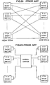
- Fig.28 is a block diagram of an ATM switch in which basic switches are interconnected.
- output ports of basic switches #11-#1N at a front stage are connected to input ports of basic switches #21-#2N at a back stage in a mesh manner.
- the number of the output ports of the basic switches #11-#1N is the same as the number of the input ports of the basic switches #21-#2N, such that the output ports are in a one-to-one correspondence with the input ports, and each of the basic switches #11-#1N selects an output port for a cell which is entered into one of the basic switches #11-#1N so that a basic switch among the basic switches #21-#2N is decided for the cell to be sent out to.
- an ATM switch of 64 inputs by 64 outputs as a whole can be realized by interconnecting 8 basic switches #11-#18 in the first stage and 8 basic switches #21-#28 in the back stage.
- Fig.29 is a block diagram showing an ATM switch in which basic switches are interconnected in a multistage manner.
- the basic switches are interconnected via WDM (wavelength division multiplexing) links by using a barrel shifter which switches signals in the WDM links according to wavelength, and, in the basic switches of the front stage, destinations of signals are determined by selecting wavelengths by which the signals are sent.
- WDM wavelength division multiplexing
- Each basic switch in the back stage is connected to every basic switch in the front stage by logical links of different wavelengths. According to the above-mentioned configuration, a number of physical links between the basic switches can be eliminated.
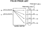
- Fig.30 shows how optical signals are switched within the barrel shifter.
- Fig.30 shows an example in which the barrel shifter has 2 input lines I0, I1 and 4 output lines 00-03.
- optical signals of wavelengths ⁇ 0 - ⁇ 3 are transmitted on each of the input lines I0, I1, and optical signals of wavelengths ⁇ 0 , ⁇ 1 , ⁇ 2 , ⁇ 3 on the input lines I0 are respectively sent to the output lines O0, O1, O2, O3.
- optical signals of wavelengths ⁇ 0 , ⁇ 1 , ⁇ 2 , ⁇ 3 on the input line I1 are respectively sent to the output lines O1, O2, O3, O0.
- a wavelength which goes to the output line O1 is ⁇ 1 among the wavelengths ⁇ 0 , ⁇ 1 , ⁇ 2 , ⁇ 3 which are transmitted on the input line I0
- a wavelength which goes to the output line O1 is ⁇ 0 among the wavelengths ⁇ 0 , ⁇ 1 ⁇ 1 , ⁇ 2 , ⁇ 3 which are transmitted on the input line I1.
- the barrel shifter is one of optical devices called "Arrayed Waveguide Grating (AWG)."
- AWG Arrayed Waveguide Grating
- FIG.31 The conceptual diagram of the AWG is shown in FIG.31.
- the AWG is made as a wavelength multiplexer-and-demultiplexer, and is an integrated on-board circuit which includes input/output waveguides and slab waveguides which act as collimators/light-gathering lenses.
- the AWG includes a plurality of different-length waveguides which are arranged at regular intervals. Similar to a diffraction grating, phase differences between the waveguides cause dispersion. Therefore, a wavelength-multiplexed signal from the input waveguide is demultiplexed, and the demultiplexed signals are extracted from different output waveguides. If the AWG is used in the reverse direction, the AWG acts as a wavelength multiplexer. Because the slab waveguide has the shape of a sector which has a center of curvature at the endpoint of the waveguide and the axis of the waveguide points to the center of curvature, the slab waveguide has a light-gathering function in a manner similar to a concave mirror. Generally, taper waveguides are inserted between the waveguides and the slab waveguide in order to decrease connection losses.
- an ordinary diffraction grating it is necessary to decrease the size of the pitch in order to increase the resolution. Therefore, the resolution is limited by the technology of the pitch making. But, regarding the AWG, a high resolution can be easily realized by increasing the diffraction order by increasing the length of the waveguide. This is the main difference between the AWG and the ordinary diffraction grating.
- a plurality of central wavelengths may exist in the AWG because the m can take any number.
- the bandwidth which can be used without overlapping is 13 nm
- WDM wavelength division multiplexing
- the barrel shifter used here is the AWG which utilizes a characteristic that same wavelength signals per bandwidth which is usable without overlapping are cyclically output as shown in FIG.32.
- FIG.33 shows an 8-input by 8-output barrel shifter.
- the barrel shifter can be used for interconnecting the above-mentioned front stage and the back stage, each of which stages includes 8 basic 8x8 switches.
- the basic switches of successive stages can be interconnected so that each switch in each stage is connected to all of the switches in the successive stage.
- FIG. 1 Another ATM switch arrangement is disclosed in the "OPTIMA: TB/S ATM Switching System Architecture based on Highly Statistical Optical WDM Interconnection" paper referred to above.
- Another known ATM switch is disclosed in WO95/24812A.
- the dynamic controller provides buffering for input data to allow data to be input while appropriate bandwidth for transfer of the data is allocated together with a connection admission control which provides information regarding available bandwidth to the dynamic bandwidth controller and the end station producing the input data to prevent cells being input to the system at too high a rate for the available bandwidth.
- the above-mentioned interconnecting part further includes a part, which is provided at each input port, for passing cells that are destined for a desired destination selectively among other cells.
- the above-mentioned interconnecting part further includes a part, which is provided at each output port, for passing cells that are destined for a desired destination selectively among other cells.
- an output port of a basic switch at the (s-1)th stage is connected to an input port of each of M basic switches belonging to a group of basic switches at the sth stage. Therefore, basic switches each of which basic switches has N (the number of groups of a stage) output ports, can be used for the ATM switch. In this way, the ATM switch which has MN 2 inputs by MN 2 outputs can be realized while each basic switch having N outputs by N outputs.
- an output port of a basic switch at the (s-1)th stage is connected to M input ports, each of which input ports belongs to each of M basic switches in a group at the sth stage, there is a connection relationship of 1:M between the output port and the input ports.
- a cell output from the output port is distributed to the M input ports. Therefore, a part for determining whether the distributed cell arriving at a basic switch is destined for the basic switch or not may be provided. The part may receive the cell if the cell is destined for the basic switch and discard the cell if not.
- the above-mentioned interconnecting part further includes a part for converting an electronic-signal cell which is output from the output port into a first wavelength-multiplexed optical signal which includes a plurality of optical signals which have different wavelengths and outputting the first wavelength-multiplexed optical signal;
- the ATM switch of the invention can be realized easily and at a low cost.
- the above-mentioned ATM switch may have a part for converting each electronic-signal cell output from the output port into an optical-signal cell which has a wavelength corresponding to the destination of the electronic-signal cell, so that a basic switch of the receiving side does not need to determine whether the arriving cell is destined for the basic switch.
- the above-mentioned ATM switch further includes a speed-conversion part for converting the speed of electronic-signal cells output from the output port. According to the invention, by decreasing the cell transmitting rate, the ATM switch can be realized at a low cost because expensive hardware for high-speed cell transmission is not necessary.
- the speed-conversion part may include at least a cell buffer, and a part for controlling the ratio between the writing clock speed of the cell buffer and a reading clock speed of the cell buffer.
- the speed-conversion part may include at least a cell buffer, and a part for controlling the ratio between the number of bit expansion data at the input side of the cell buffer and the number of bit expansion data at the output side of the cell buffer.
- the cell transmitting rate can be decreased.
- the ATM switch may include a monitoring part for monitoring the arriving rate of the electronic-signal cells output from the output port, and a part for converting the speed of the electronic-signal cells according to the arriving rate.
- a burst of cells can be distributed to cells at an average cell rate. Therefore, the capacity of a cell buffer downstream from the cell buffer having the monitoring part can be decreased by avoiding receiving the burst of cells.
- the ATM switch may further includes a detecting part for detecting traffic congestion of a route between the basic switches by using the monitored cell rate, and a part for prohibiting the ATM switch from establishing an ATM connection on the route in which the traffic congestion is detected.
- discarded cells can be decreased within the ATM switch because an ATM connection is not established on a congested route.
- the monitoring part and the detecting part may be provided at the input port of the basic switch.
- the ATM switch may further include:
- information of congestion can be transmitted within the ATM switch without using a link specifically for the information.
- the ATM connections can be controlled within the whole ATM switch, and the destination of the information of congestion can be limited to the input port. Therefore, the transmission can be performed easily.
- the ATM switch of MN 2 inputs by MN 2 outputs can be realized easily and at a low cost without increasing the number of ports of the basic switch and the number of the wavelengths. Further, by decreasing the cell transmission rate using the speed-conversion part, by converting incoming cells at unbalanced intervals into cells at balanced intervals, and by establishing routes according to ATM service classes, and so on, the hardware configuration can be more simple and can be realized at a lower cost.
- an ATM switch according to the present invention has M ⁇ N basic switches #111-#1MN at a front stage and M ⁇ N basic switches #211-#2MN at a back stage, and each basic switch has N input ports and N output ports. Then, the basic switches #111-#1MN and the basic switches #211-#2MN are interconnected, which results in forming the ATM switch of M ⁇ N 2 inputs by M ⁇ N 2 outputs.
- the M ⁇ N basic switches #111-#1MN at the front stage are divided into N switch groups A1-N1, where each group has M basic switches
- the M ⁇ N basic switches #211-#2MN at the back stage are divided into N switch groups A2-N2, where each group also has M basic switches.
- the ATM switch includes 512 sender ports 10 each of which sender ports is connected to each output port of each basic switch at the front stage, 512 receiver ports 20, each of which receiver ports is connected to each input port of each basic switch at the back stage, and 64 barrel shifters 30-1 to 30-64, each of which barrel shifters is provided between 8 sender ports connected to the jth output ports of the basic switch #lki (each of j and k is an integer, 1 j,k 8) belonging to the ith (i is an integer, 1 i 8) group of the front stage and 8 receiver ports connected to ith input ports of the basic switch #2kj belonging to the jth group of the back stage.
- the sender port 10 converts an electronic-signal cell sent out from the output port into 8 optical-signal cells having 8 different wavelengths, and wavelength-multiplexes the optical-signal cells into wavelength-multiplexed optical signal .
- the receiver port 20 demultiplexes the arriving wavelength-multiplexed optical signal into 8 optical-signal cells having 8 different wavelengths, and converts each of the 8 optical-signal cells into an electronic-signal cell.
- the barrel shifter receives 8 wavelength-multiplexed optical signals from 8 sender ports, and switches wavelengths of the wavelength-multiplexed optical signals, then sends 8 wavelength-switched-optical signals to the 8 receiver ports.
- Fig.3 shows a wavelength switching table.
- 8 ⁇ 8 (8-input by 8-output) basic switches #111-#288 are interconnected by using 8 ⁇ 8 (8-input by 8-output) barrel shifters 30-1 to 30-64.
- 64 basic switches #111-#188 of the front stage and 64 basic switches #211-#288 of the back stage are interconnected by using 64 barrel shifters 30-1 to 30-64.
- the basic switches #111-#188 are divided into 8 groups (A1-H1), each of which groups includes 8 basic switches, and the basic switches #211-#288 are similarly divided into 8 groups (A2-H2), each of which groups includes 8 basic switches.
- a cell which is entered into an input port of a basic switch at the front stage is routed to one of the groups (A2-H2) at the back stage according to the position of the output port of the basic switch at the front stage, where the cell routes through the output port.
- one of the groups (A2-H2) of the basic switches #211-#288 at the back stage can be selected for the cell.
- a wavelength-multiplexed optical signal which includes 8 wavelengths is sent out from the sender port 10 which is connected to the jth output port of the basic switch #1ki at the front stage, and the wavelength-multiplexed optical signal is entered into the barrel shifter 30-((j-1)X8+i). Then, optical signals of the wavelength-multiplexed optical signal are switched according to wavelength within the barrel shifter according to the table shown in Fig.3 and divided into 8 wavelength-multiplexed optical signals. After that, the 8 wavelength-multiplexed optical signals are sent to the basic switches #21j-#28j at the back stage respectively. Finally, each of the receiver ports 20 connected to the input ports of the basic switches #21j-#28j receives one of the 8 wavelength-multiplexed optical signals.
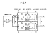
- Fig.4 is a block diagram of sender ports according to the first embodiment of the present invention.
- the sender port 10 converts an electronic-signal cell sent out from the output port into 8 optical-signal cells having 8 different wavelengths, wavelength-multiplexes the optical-signal cells into wavelength-multiplexed optical signal, and then outputs the signal through an optical fiber.
- the electronic-signal cell sent out from the output port of the basic switch #lki at the front stage is divided into 8 electronic-signal cells after entering into the sender port 10, and each of the 8 electronic-signal cells is converted into the optical-signal cell having its own wavelength by an E/O converter 11.
- the 8 optical-signal cells are wavelength-multiplexed by a wavelength multiplexer 12, and then the wavelength-multiplexed optical signal is sent out through the optical fiber.
- a laser diode is used for the E/O converter 11, but various known converters can be used.
- various known multiplexers can be used for the 8-wavelength multiplexer 12, various known multiplexers can be used.
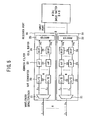
- Fig.5 is a block diagram of the receiver ports.
- the receiver port 20 demultiplexes the arriving 8-wavelength-multiplexed optical signal into 8 optical-signal cells having 8 different wavelengths, converts the 8 optical-signal cells into 8 electronic-signal cells, and then selects a cell destined for the connected input port of the basic switch #2kj among the 8 cells and sends out the selected cell to the input port.
- the receiver port 20 includes an 8-wavelength demultiplexer 21, O/E converters 22, address filters 23, cell buffers 24, and a cell-arbiter 25.
- O/E converters Various known wavelength demultiplexers can be used for the wavelength demultiplexer 21.
- a laser diode is used for the O/E converter 22 in the embodiment, but various converters can be used.
- the incoming 8-wavelength-multiplexed optical signal is wavelength-demultiplexed into 8 optical-signal cells having 8 different wavelengths by the wavelength demultiplexer 21, and the optical-signal cells are converted into electronic-signal cells by the O/E converters 22, then a cell destined for the connected input port of the basic switch #2kj is selected by the address filters 23 among the cells.
- the selected cell is stored in the cell buffer 24, and, then, the cell-arbiter 25 arbitrates the cell buffers 24 and sends out the cell to the input port of the basic switch #2kj at the back stage.
- a cell which is destined for the basic switch #211 which cell is outgoing from a port which is destined for group A2 determines the port by checking out routing-bits within the cells.
- the top port of the basic switch #118 shown in Fig.2 corresponds to the port.
- the cell sent from the top port is divided into 8 signals each of which has a different wavelength at the barrel shifter, the 8 signals go to the bottom input ports of the 8 basic switches #211-#281, and, then, only the basic switch #211 gets the cell through the address filter 23.
- Fig.6 is a block diagram of sender ports 10 according to the second embodiment of the present invention.
- the sender port 10 has a wavelength-selection switch 13 for selecting a wavelength by which the electronic-signal cell incoming from the connected output port of the basic switch #lki is converted into the optical-signal cell.
- the wavelength-selection-switch 13 After receiving the electronic-signal cell, the wavelength-selection-switch 13 reads information of the destination of the cell, and, then, the wavelength-selection-switch 13 outputs the cell to the E/O converter 11 which uses a wavelength corresponding to the destination. In this way, the electronic-signal cell is converted to an optical-signal cell having the wavelength corresponding to the desired destination.
- Fig.7 is a block diagram of the receiver ports 20 according to the second embodiment of the present invention.
- the incoming 8-wavelength-multiplexed optical signal is wavelength-demultiplexed into 8 optical-signal cells having 8 different wavelengths by the wavelength demultiplexer 21, and the optical-signal cells are converted into electronic-signal cells by the O/E converters.
- a wavelength corresponding to a cell's destination has been assigned to each cell. In other words, only cells destined for an input port to which the receiver port 20 is connected enter into the receiver port. Therefore, the cell switch 26 simply outputs the electronic-signal-sells in sequence to the input port.
- a cell which is destined for the basic switch #211 determines a port which is destined for group A2 by checking out its routing-bits within the cells. Further, within the sender port 10, a wavelength ⁇ 1 which is used for a channel to the basic switch #211 of the group A2 is assigned to the cell. Then, the cell converted into an optical-signal cell of the wavelength ⁇ 1 is routed to the basic switch #211.
- the sender port 10 has speed-conversion buffers 40.
- Fig.8 shows the sender port which includes the speed-conversion-buffers 40 in the sender port of the first embodiment
- Fig.9 shows the sender port which includes the speed-conversion-buffers 40 in the sender port of the second embodiment.
- the speed-conversion-buffer includes a write controller 41, a clock converter 42, a read controller 43 and a cell buffer 44.
- the transmission rate of the cells written into and read out of the cell buffer 44 is converted by controlling a writing clock and a reading clock.
- Another example of the speed-conversion-buffer 40 includes a read-write controller 45 and the cell buffer 44.
- the transmission rate of the cells is converted by controlling the number of bit expansion data at the input side and the output side of the cell buffer 44. More precisely, the read-write controller 45 replaces headers of incoming 16 bit expansion data with new headers, then, 4 bit expansion data is sent out from the cell buffer 44, and, as a result, the rate is converted.
- an ATM switch can be realized at a low cost without using any hardware for a high-speed cell transmission.
- Fig.12 is a diagram of a 3-stage ATM switch according to an embodiment of the present invention.
- One of the reasons for increasing the number of stages is that the number of available connections increases so as to distribute cell-traffic within the ATM switch.
- the 3-stage-ATM switch it is possible to select a route among various routes per each ATM connection.
- an ATM cell sent out from line unit (LU) 100 is transferred to an LU102 through one of a plurality of routes shown in Fig.12.
- the ATM connections are configured so as to equalize the cell rate of each wavelength channel. For example, if the bandwidth of a port is 10 Gbps, the equalized average cell rate at which each wavelength signal transmits the cells is 1.25-Gbps. The configuration will be described more precisely later.
- Fig.13 shows a part of the output port 104 shown in Fig.12. Also, the figure shows a part of the wavelength-selection switch and the speed-conversion buffer of the sender port shown in Fig.9.
- an incoming signal at a rate of 10 Gbps is divided, and the divided signals are entered into each of buffers 108-115.
- the rate of each signal is converted in the above-mentioned way, and goes out at a rate of 2.5 Gbps.
- Fig.15 is a block diagram of the speed-conversion buffer of the fourth embodiment of the present invention
- Fig.16 is a diagram showing an operation of the fourth embodiment of the present invention.
- a traffic monitor 46 is provided at the input side of the cell buffer 44.
- the traffic monitor 46 monitors the rate of the incoming cells and sends cell rate information to the read-write controller 45. According to the cell rate information, the read-write controller 45 converts the rate of the cells in such a way described in the third embodiment.
- the traffic monitor detects the unbalance, and, then, the read-write controller 45 controls the rate of the cells so that the cell buffer 44 sends the cells at balanced intervals.
- the buffer capacity of the cell buffer 24 of the receiver port 20 which receives the cells from the sender port 10 having the speed-conversion-buffer 40 can be decreased.
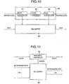
- Fig.17 is a block diagram of the fifth embodiment of the present invention
- Fig.18 is a diagram showing a 3-stage ATM switch according to the fifth embodiment of the present invention.
- a connection-route managing part 47 which is connected to the traffic monitor 46 is provided.
- the above-mentioned cell rate information is sent to the connection-route managing part 47 from the traffic monitor 46, and the connection-route-managing-part 47 manages the configuration of each connection within the ATM switch.
- the connection-route-managing-part 47 manages the traffic so that the cells are distributed equally to each ATM connection within the ATM switch.
- the rate of the cells can be decreased as a whole because the cells are not gathered intensively at a few ATM connections. According to the above configuration, by decreasing the rate of the cells, an ATM switch can be realized at a low cost without using any hardware for a high-speed cell transmission.
- the cells within a multistage (in this case, 3-stage) ATM switch can be distributed among the ATM connections by performing the configuration management of the ATM connections with the traffic monitor 46 and the connection-route managing part 47 being provided, for example, at each sender port.
- At least one sender port that has the speed-conversion buffer 40 (hereinafter, called a first sender port) is used in combination with at least one sender port that does not have it (hereinafter, called a second sender port), in which the sum of the number of the sender ports is 8, which sender ports are to be connected to a basic switch at the front stage.
- a first sender port At least one sender port that has the speed-conversion buffer 40
- a second sender port in which the sum of the number of the sender ports is 8, which sender ports are to be connected to a basic switch at the front stage.
- an ATM connection transmitting cells at a high peak cell rate uses the high-speed route
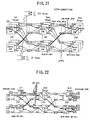
- an ATM connection transmitting cells at a low peak cell rate uses the low-speed route. Therefore, as shown in Fig.21, even in the case of various existing cell rates each of which rates is different according to an ATM service class, by setting up routes according to the cell rates, an ATM switch being adapted efficiently to various ATM service classes can be realized.
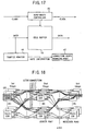
- Fig.22 is a diagram of a 3-stage ATM switch for explaining transmission of RM (Resource Management) cells within the 3-stage-ATM switch.
- the 3-stage-ATM switch has line units (LUs) connected to each input port of each basic switch at the first stage and to each output port of each basic switch at the third stage on a one-by-one basis.
- a line unit at the first stage periodically sends the RM cells to a line unit at the third stage through various routes, and, then, after it receives the RM cells, it sends back the RM cells to the line unit at the first stage.
- the connection-route managing part 47 at each basic switch on each route can obtain information on the incoming cell rate of each basic switch.
- every basic switch associated with an ATM connection can distribute the cells of the ATM connection equally to various routes in close liaison with each other, which is different from in the case of the fifth embodiment in which each basic switch autonomously distributes the cells of an ATM connection associated with the basic switch.
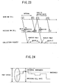
- Fig.23 is a diagram for explaining route management of ATM connections at the line unit.
- the line unit provided at the input port (of the first stage of a multistage ATM switch as shown in Fig.22) monitors traffic of routes connected to the input port, and, if the line unit detects a congested route, the line unit replaces headers of incoming cells so as to route the cells through another route.
- the line unit reads out information on the congestion, and rewrites an inside-header adding table according to the information so that a header representing the congested route should not be added to the incoming cells, and, then, the line unit can establish a route alternative to the congested route.
- the RM cells are sent out from the line unit at established intervals to each route, and, as shown in (b), for example, if the line unit detects that a route B is congested, it rewrites the inside-header adding table so as to avoid the congested route as shown in (c).
- Fig.24 is a diagram for explaining a relationship between a residual bandwidth and a threshold
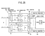
- Fig.25 is a block diagram showing the case in which the traffic monitors are provided at input ports.
- a threshold of a residual bandwidth of a port is established. If the residual bandwidth is lower than the threshold, the line unit decides that traffic congestion occurs, and, then, the line unit sends the RM cell with the congestion information so as to avoid establishing an ATM connection on the congested route.
- the traffic monitor may be provided at an input port side of the back stage.
- a congested condition of a route also can be detected as in the case of providing the traffic monitor at an output port side as shown in Fig.17.
- FIG.26 A tenth embodiment of the present invention will be described with reference to Fig.26 and Fig.27 in the following.
- FIG.26 and Fig.27 is a block diagram of receiver ports which are realized by CMOS LSI circuits.
- the receiver port uses a shared buffer instead of a cell switch 26 shown in Fig.25 and includes a traffic monitor 46 within the receiver port.
- Cell-identifying parts 51, the shared buffer 50 and the traffic monitor 46 can be realized by a CMOS LSI circuit.
- the cell-identifying part 51 has not been shown in the figures so far for the sake of simplicity, but it is necessary to provide it next to the O/E converter 22.
- the shared buffer 50 temporarily stores the electronic-signal cells and the cells are successively read out from the shared buffer 50.
- the circuit size can be reduced by using such a shared buffer.
- a receiver port may have the shared buffer 50 instead of the cell buffers 24 and the arbiter 25 of the receiver port shown in Fig.5.
- the cell-identifying parts 51, the address filters 23 and the shared buffer 50 can also be realized by a CMOS LSI circuit.
- the ATM switch it is possible to increase routes of cells by converting a cell being output from each output port of each basic switch #1ki at the front stage into a wavelength-multiplexed signal including the same number of wavelengths as the number of basic switches of one group at the back stage. Therefore, the number of basic switches which can be connected can be increased.
- the size of the ATM switch is expanded to M times when compared to a conventional ATM switch. More precisely, in a conventional technology in which M ⁇ M basic switches and M-wavelength-multiplexing links are used, the number of ports can be expanded to M 2 at most. However, according to the present invention, it can be expanded to M 3 .
- the ATM switch having MN 2 inputs by MN 2 outputs can be realized by using N ⁇ N basic switches, in other words, because there is no need to change the number of ports of the basic switches, a large-scale ATM switch can be realized easily and at a low cost.
- the hardware configuration can be more simple and can be realized at a lower cost.
- the scale of an ATM switch can be expanded without increasing the number of ports of the basic switch and the number of the wavelengths.
- the hardware especially, the part situated at the back of the sender port, can be realized at a low cost.
- the size of buffers can be reduced, and a plurality of ATM connections of different ATM service classes are efficiently accommodated into the ATM switch. Furthermore, congestion in the ATM connections can be reduced.
Landscapes
- Engineering & Computer Science (AREA)
- Computer Networks & Wireless Communication (AREA)
- Signal Processing (AREA)
- Physics & Mathematics (AREA)
- Electromagnetism (AREA)
- Data Exchanges In Wide-Area Networks (AREA)
- Optical Communication System (AREA)
- Use Of Switch Circuits For Exchanges And Methods Of Control Of Multiplex Exchanges (AREA)
Claims (19)
- ATM-Koppelfeld mit S Stufen, wobei S eine ganze Zahl ist und 2 ≤ S gilt,
wobei die jeweilige Stufe eine Vielzahl von Grund-Koppelfeldern (#111-#1MN, #211-#2MN) enthält,
wobei das betreffende ATM-Koppelfeld M x N Grund-Koppelfelder pro jeweiliger Stufe enthält, wobei M und N jeweils eine positive ganze Zahl ist, die größer ist als 1, und eine Verbindungseinrichtung zur Verbindung der jeweiligen Stufen miteinander aufweist,
dadurch gekennzeichnet, dass die genannten M x N Grund-Koppelfelder N Gruppen aufweisen und dass die Verbindungseinrichtung einen j-ten Ausgangsanschluss (10) des jeweiligen Grund-Koppelfeldes, welches zu einer i-ten Gruppe in einer (s-1)-ten Stufe gehört, mit zumindest einem i-ten Eingangsanschluss (20) der Grund-Koppelfelder verbindet, die zu einer j-ten Gruppe in einer s-ten Stufe gehören,
wobei j, i und s positive ganze Zahlen sind und wobei 1 ≤ j ≤ N, 1 ≤ i ≤ N, 2 ≤ s ≤ S gilt. - ATM-Koppelfeld nach Anspruch 1,
dadurch gekennzeichnet, dass die genannte Verbindungseinrichtung eine Einrichtung (26) enthält, die an dem jeweiligen Eingangsanschluss zur Weiterleitung solcher Zellen vorgesehen ist, die selektiv unter anderen Zellen für ein gewünschtes Ziel bestimmt sind. - ATM-Koppelfeld nach Anspruch 1,
dadurch gekennzeichnet, dass die genannte Verbindungseinrichtung eine Einrichtung (13) enthält, die an dem jeweiligen Ausgangsanschluss zur Weiterleitung solcher Zellen vorgesehen ist, die selektiv unter anderen Zellen für ein gewünschtes Ziel bestimmt sind. - ATM-Koppelfeld nach Anspruch 1,
dadurch gekennzeichnet, dass die genannte Verbindungseinrichtung eine Einrichtung (11, 12) zur Umsetzung einer elektronischen Signalzelle, die von dem genannten Ausgangsanschluss abgegeben wird, in ein erstes optisches Wellenlängen-Multiplexsignal, welches eine Vielzahl von optischen Signalen enthält, die unterschiedliche Wellenlängen aufweisen, und zur Abgabe des ersten optischen Wellenlängen-Multiplexsignals,
eine Einrichtung (30) zur Erzeugung eines zweiten optischen Wellenlängen-Multiplexsignals durch Vermittlung von optischen Signalen und Abgabe des zweiten optischen Wellenlängen-Multiplexsignals
und eine Einrichtung (21-25) zur Umsetzung des genannten zweiten optischen Wellenlängen-Multiplexsignals in elektronische Signalzellen und zur Ein- bzw. Abgabe zumindest einer der betreffenden elektronischen Signalzellen an den Eingangsanschluss aufweist. - ATM-Koppelfeld nach Anspruch 1,
dadurch gekennzeichnet, dass die genannte Verbindungseinrichtung eine Einrichtung (11) zur Umsetzung einer ersten elektronischen Signalzelle, die von dem genannten Ausgangsanschluss abgegeben ist, in N optische Signalzellen, die unterschiedliche Wellenlängen aufweisen,
eine Wellenlängen-Multiplexeinrichtung (12) zur Erzeugung eines optischen Wellenlängen-Multiplexsignals durch Wellenlängen-Multiplexverarbeitung der genannten N optischen Signalzellen,
eine Wellenlängen-Demultiplexeinrichtung (21) zur Wellenlängen-Demultiplexverarbeitung eines optischen Wellenlängen-Multiplexsignals in N optische Signalzellen, die unterschiedliche Wellenlängen aufweisen,
eine Einrichtung (22) zur Umsetzung der genannten N optischen Signalzellen in N zweite elektronische Signalzellen,
eine Eingabe- bzw. Eingangseinrichtung (25) zur Ein- bzw. Abgabe zumindest einer der genannten zweiten elektronischen Signalzellen an den genannten Eingangsanschluss
und eine Wellenlängen-Vermittlungseinrichtung (30) zum Vermitteln von optischen Signalen der M optischen Wellenlängen-Multiplexsignale umfasst, die von der genannten Wellenlängen-Multiplexeinrichtung her eintreffen, und zur Abgabe der vermittelten optischen Wellenlängen-Multiplexsignale an die genannte Wellenlängen-Demultiplexeinrichtung,
wobei die genannte Wellenlängen-Vermittlungseinrichtung zwischen der genannten Wellenlängen-Multiplexeinrichtung, welche an den j-ten Ausgangsanschlüssen der genannten Grund-Koppelfelder angeschlossen ist, die zu der i-ten Gruppe in der (s-1)-ten Stufe gehören, und der genannten Wellenlängen-Demultiplexeinrichtung vorgesehen ist, die an den i-ten Eingangsanschlüssen der Grund-Koppelfelder angeschlossen sind, welche zu der genannten j-ten Gruppe in der s-ten Stufe gehören. - ATM-Koppelfeld nach Anspruch 5,
dadurch gekennzeichnet, dass die genannte Eingabe- bzw. Eingangseinrichtung eine Einrichtung (26) zur Weiterleitung lediglich solcher elektronischer Signalzellen umfasst, die selektiv aus den genannten elektronischen Signalzellen für ein gewünschtes Ziel bestimmt sind. - ATM-Koppelfeld nach Anspruch 5,
dadurch gekennzeichnet, dass es ferner eine Einrichtung (11, 12, 13) zur Umsetzung der von dem genannten Abgabe- bzw. Ausgangsanschluss abgegebenen jeweiligen elektronischen Signalzelle in eine optische Signalzelle umfasst, die eine dem Ziel der elektronischen Signalzelle entsprechende Wellenlänge aufweist. - ATM-Koppelfeld nach Anspruch 5,
dadurch gekennzeichnet, dass die genannte Wellenlängen-Vermittlungseinrichtung eine Schiebelogikschaltung (Barrel-Shifter) enthält, die imstande ist, ein optisches Signal einer p-ten Wellenlänge, wobei p=1,2...N gilt, in dem m-ten optischen Wellenlängen-Multiplexsignal, wobei m=1,2...M gilt, zu bzw. an einem (m+p)-ten Ausgang der Schiebelogikschaltung abzugeben, wobei in dem Fall, dass m+p gegeben ist mit k und k eine ganze Zahl ist, die größer ist als die Anzahl der genannten Wellenlängen-Demultiplexeinrichtungen, die betreffende Schiebelogikschaltung das optische Signal zu bzw. an einem ((m+p)-k)-ten Ausgang der Schiebelogikschaltung abgibt. - ATM-Koppelfeld nach Anspruch 1,
dadurch gekennzeichnet, dass es ferner eine Geschwindigkeits-Umsetzungseinrichtung (40) zur Umsetzung der Geschwindigkeit der von dem genannten Abgabe- bzw. Ausgangsanschluss abgegebenen elektronischen Signalzellen aufweist. - ATM-Koppelfeld nach Anspruch 9,
dadurch gekennzeichnet, dass die genannte Geschwindigkeits-Umsetzungseinrichtung zumindest einen Zellpuffer (44) und eine Einrichtung (42, 43) zur Steuerung des Verhältnisses zwischen der Schreibtaktgeschwindigkeit des Zellpuffers und der Lesetaktgeschwindigkeit des Zellpuffers aufweist. - ATM-Koppelfeld nach Anspruch 9,
dadurch gekennzeichnet, dass die genannte Geschwindigkeits-Umsetzungseinrichtung zumindest einen Zellpuffer (44) und eine Einrichtung (45) zur Steuerung des Verhältnisses zwischen der Anzahl von Bit-Dehnungsdaten auf der Eingangsseite des Zellpuffers und der Anzahl von Bit-Dehnungsdaten auf der Ausgangsseite des Zellpuffers aufweist. - ATM-Koppelfeld nach Anspruch 1,
dadurch gekennzeichnet, dass es ferner eine Einrichtung (46) zur Überwachung der Ankunftsrate der von dem genannten Abgabe- bzw. Ausgangsanschluss abgegebenen elektronischen Signalzellen und eine Einrichtung (44, 45) zur Umsetzung der Geschwindigkeit der elektronischen Signalzellen entsprechend der Ankunftsrate aufweist. - ATM-Koppelfeld nach Anspruch 1,
dadurch gekennzeichnet, dass es ferner zumindest einen Zellpuffer (44), der imstande ist, die von dem genannten Abgabe- bzw. Ausgangsanschluss abgegebenen elektronischen Signalzellen zwischenzuspeichern,
eine Einrichtung (46) zur Überwachung der Rate der betreffenden elektronischen Signalzellen, die an dem genannten Zellpuffer ankommen,
und eine Einrichtung (47) zur Festlegung bzw. Errichtung einer Vielzahl von ATM-Verbindungen zwischen den genannten Grund-Koppelfeldern aufweist, derart, dass die Zell-Übertragungsraten der ATM-Verbindungen durch Heranziehen der Ankunftsrate ausgeglichen werden. - ATM-Koppelfeld nach Anspruch 9,
dadurch gekennzeichnet, dass es ferner eine Einrichtung zur Festlegung bzw. Errichtung von Routen von ATM-Verbindungen enthält, die eine Vielzahl von Dienstklassen aufweisen. - ATM-Koppelfeld nach Anspruch 1,
dadurch gekennzeichnet, dass es ferner eine Überwachungseinrichtung (46) zur Überwachung der Ankunftsrate der genannten elektronischen Signalzellen,
eine Detektiereinrichtung (46) zur Ermittlung eines Verkehrsstaus auf einer Route zwischen den genannten Grund-Koppelfeldern durch Heranziehen der Ankunftsrate
und eine Einrichtung umfasst, welche das ATM-Koppelfeld daran hindert, eine ATM-Verbindung auf der Route festzulegen bzw. zu errichten, auf der der betreffende Verkehrsstau ermittelt ist. - ATM-Koppelfeld nach Anspruch 15,
dadurch gekennzeichnet, dass die Überwachungseinrichtung und die Detektiereinrichtung am Eingangsanschluss des Grund-Koppelfeldes vorgesehen sind. - ATM-Koppelfeld nach Anspruch 15,
dadurch gekennzeichnet, dass die Detektiereinrichtung eine Einrichtung zur Übertragung des Ergebnisses der Ermittlung zu zumindest einem Grund-Koppelfeld enthält. - ATM-Koppelfeld nach Anspruch 1,
dadurch gekennzeichnet, dass es ferner eine Überwachungseinrichtung (46) zur Überwachung der Restbandbreite eines Anschlusses des genannten Grund-Koppelfeldes,
eine Einrichtung (46) zur Aussendung einer RM- bzw. Ressourcen-Management-Zelle auf einer Vielzahl von Routen,
eine Rücksendeeinrichtung für den Empfang und die Rücksendung der RM-Zelle
und eine Unterbindungseinrichtung enthält, die das ATM-Koppelfeld an der Festlegung bzw. Errichtung einer ATM-Verbindung auf einer bestimmten Route entsprechend der zurückgesandten RM-Zelle hindert,
wobei in dem Fall, dass die betreffende Überwachungseinrichtung feststellt, dass die Restbandbreite kleiner ist als ein bestimmter Wert, die genannte Rücksendeeinrichtung eine Information bezüglich eines Verkehrsstaus in die RM-Zelle einschließt und die RM-Zelle zurücksendet,
und wobei die genannte Unterbindungseinrichtung das ATM-Koppelfeld an der Festlegung bzw. Errichtung einer ATM-Verbindung auf einer Route hindert, die durch den Inhalt der zurückgesandten RM-Zelle angegeben ist. - ATM-Koppelfeld nach Anspruch 18,
dadurch gekennzeichnet, dass die genannte Unterbindungseinrichtung eine Einrichtung enthält, die einen Header zur Meidung einer verstopften Route zu einer Zelle entsprechend dem Inhalt der RM-Zelle hinzufügt.
Priority Applications (1)
| Application Number | Priority Date | Filing Date | Title |
|---|---|---|---|
| EP05003631A EP1542413B1 (de) | 1998-03-05 | 1999-03-02 | Optische Verbindungen in einer ATM-Vermittlungsstelle |
Applications Claiming Priority (6)
| Application Number | Priority Date | Filing Date | Title |
|---|---|---|---|
| JP5381598 | 1998-03-05 | ||
| JP5381598 | 1998-03-05 | ||
| JP20078098 | 1998-07-15 | ||
| JP20078098 | 1998-07-15 | ||
| JP1877799 | 1999-01-27 | ||
| JP1877799 | 1999-01-27 |
Related Child Applications (1)
| Application Number | Title | Priority Date | Filing Date |
|---|---|---|---|
| EP05003631A Division EP1542413B1 (de) | 1998-03-05 | 1999-03-02 | Optische Verbindungen in einer ATM-Vermittlungsstelle |
Publications (3)
| Publication Number | Publication Date |
|---|---|
| EP0949837A2 EP0949837A2 (de) | 1999-10-13 |
| EP0949837A3 EP0949837A3 (de) | 2004-08-11 |
| EP0949837B1 true EP0949837B1 (de) | 2005-11-16 |
Family
ID=27282356
Family Applications (2)
| Application Number | Title | Priority Date | Filing Date |
|---|---|---|---|
| EP05003631A Expired - Lifetime EP1542413B1 (de) | 1998-03-05 | 1999-03-02 | Optische Verbindungen in einer ATM-Vermittlungsstelle |
| EP99301545A Expired - Lifetime EP0949837B1 (de) | 1998-03-05 | 1999-03-02 | ATM Koppelfeld |
Family Applications Before (1)
| Application Number | Title | Priority Date | Filing Date |
|---|---|---|---|
| EP05003631A Expired - Lifetime EP1542413B1 (de) | 1998-03-05 | 1999-03-02 | Optische Verbindungen in einer ATM-Vermittlungsstelle |
Country Status (3)
| Country | Link |
|---|---|
| US (1) | US6570874B1 (de) |
| EP (2) | EP1542413B1 (de) |
| DE (2) | DE69928315T2 (de) |
Families Citing this family (29)
| Publication number | Priority date | Publication date | Assignee | Title |
|---|---|---|---|---|
| US6580537B1 (en) | 1998-07-17 | 2003-06-17 | Regents Of The University Of California, The | High-throughput, low-latency next generation internet networks using optical label switching and high-speed optical header generation, detection and reinsertion |
| US6525850B1 (en) | 1998-07-17 | 2003-02-25 | The Regents Of The University Of California | High-throughput, low-latency next generation internet networks using optical label switching and high-speed optical header generation, detection and reinsertion |
| US6111673A (en) | 1998-07-17 | 2000-08-29 | Telcordia Technologies, Inc. | High-throughput, low-latency next generation internet networks using optical tag switching |
| US6519062B1 (en) | 2000-02-29 | 2003-02-11 | The Regents Of The University Of California | Ultra-low latency multi-protocol optical routers for the next generation internet |
| US6853635B1 (en) * | 2000-07-24 | 2005-02-08 | Nortel Networks Limited | Multi-dimensional lattice network |
| US6757497B2 (en) | 2001-01-30 | 2004-06-29 | The Regents Of The University Of California | Optical layer multicasting using a single sub-carrier header and a multicast switch with active header insertion via reflective single sideband optical processing |
| US6768871B2 (en) | 2001-01-30 | 2004-07-27 | The Regents Of The University Of California | Optical layer multicasting using a multicast switch to effect survivability and security |
| US6754450B2 (en) | 2001-01-30 | 2004-06-22 | The Regents Of The University Of California | Optical layer multicasting using a single sub-carrier header with active header detection, deletion, and new header insertion via opto-electrical processing |
| US6850515B2 (en) | 2001-01-30 | 2005-02-01 | The Regents Of The University Of California | Optical layer multicasting using a single sub-carrier header and a multicast switch with active header insertion via light circulation |
| US6819666B2 (en) | 2001-01-30 | 2004-11-16 | The Regents Of The University Of California | Optical layer multicasting using multiple sub-carrier headers with header detection, deletion, and insertion via reflective single sideband optical processing |
| US6813276B2 (en) | 2001-01-30 | 2004-11-02 | The Regents Of The University Of California | Optical layer multicasting using a single sub-carrier header with active header detection, deletion, and re-insertion via a circulating optical path |
| US6757496B2 (en) | 2001-01-30 | 2004-06-29 | The Regents Of The University Of California | Optical layer multicasting using a single sub-carrier header and an optical multicasting switch |
| US6850707B1 (en) | 2001-01-30 | 2005-02-01 | The Regents Of The University Of California | Secure optical layer multicasting to effect survivability |
| US6873797B2 (en) | 2001-01-30 | 2005-03-29 | The Regents Of The University Of California | Optical layer multicasting |
| US20020126349A1 (en) * | 2001-03-12 | 2002-09-12 | Mohsen Sarraf | Multiplexing information on multiple wavelengths in optical systems |
| US7174065B2 (en) | 2002-03-21 | 2007-02-06 | Avago Technologies Fiber Ip (Singapore) Pte. Ltd. | Optical switching fabric with an optical to electrical converter in the output plane |
| US20050031250A1 (en) * | 2003-08-07 | 2005-02-10 | Schroeder Dale W. | Multistage optical switch |
| JP4501697B2 (ja) * | 2005-01-21 | 2010-07-14 | 日本電気株式会社 | コアネットワークシステム及び光伝送装置 |
| JP4638754B2 (ja) * | 2005-03-18 | 2011-02-23 | 富士通株式会社 | 光装置および光クロスコネクト装置 |
| US20080247387A1 (en) * | 2007-04-09 | 2008-10-09 | Neilson David T | Scalable hybrid switch fabric |
| US20090324243A1 (en) * | 2008-06-30 | 2009-12-31 | Lucent Technologies Inc. | Scalable load-balanced interconnect switch based on an optical switch fabric having a bank of wavelength-selective switches |
| US20090324221A1 (en) * | 2008-06-30 | 2009-12-31 | Lucent Technologies Inc. | Scalable load-balanced interconnect switch based on an arrayed waveguide grating |
| US20080282550A1 (en) * | 2008-06-30 | 2008-11-20 | Andis Company | Blade assembly |
| US10491973B2 (en) | 2015-04-24 | 2019-11-26 | Rockley Photonics Limited | Optoelectronic switch |
| US9900672B2 (en) | 2015-04-24 | 2018-02-20 | Rockley Photonics Limited | Optoelectronic switch architectures |
| WO2016170357A1 (en) * | 2015-04-24 | 2016-10-27 | Rockley Photonics Limited | Optoelectronic switch architectures |
| CN107852261B (zh) * | 2015-04-24 | 2019-06-25 | 洛克利光子有限公司 | 光电开关架构 |
| CN108370279B (zh) | 2015-09-29 | 2020-04-14 | 洛克利光子有限公司 | 光电交换机 |
| KR20180042631A (ko) * | 2016-10-18 | 2018-04-26 | 한국전자통신연구원 | 포토닉 프레임 처리 장치 및 방법 |
Family Cites Families (7)
| Publication number | Priority date | Publication date | Assignee | Title |
|---|---|---|---|---|
| US5077483A (en) * | 1989-05-08 | 1991-12-31 | At&T Bell Laboratories | Network topology for reduced blocking and photonic system implementation thereof |
| JP3173551B2 (ja) | 1993-07-14 | 2001-06-04 | 日本電信電話株式会社 | 光周波数ルーチング型時分割ハイウェイスイッチ |
| JPH0787097A (ja) | 1993-09-13 | 1995-03-31 | Toshiba Corp | 光交換回路 |
| US5504744A (en) * | 1994-03-09 | 1996-04-02 | British Telecommunications Public Limited Company | Broadband switching network |
| JP2571025B2 (ja) * | 1994-10-13 | 1997-01-16 | 日本電気株式会社 | 網内光終端ノード |
| FR2735638B1 (fr) * | 1995-06-14 | 1997-07-11 | Cit Alcatel | Matrice de commutation a mode de transfert asynchrone, de grande capacite |
| JPH1013867A (ja) | 1996-06-26 | 1998-01-16 | Nippon Telegr & Teleph Corp <Ntt> | 光パケットスイッチ |
-
1999
- 1999-03-02 EP EP05003631A patent/EP1542413B1/de not_active Expired - Lifetime
- 1999-03-02 DE DE69928315T patent/DE69928315T2/de not_active Expired - Fee Related
- 1999-03-02 EP EP99301545A patent/EP0949837B1/de not_active Expired - Lifetime
- 1999-03-02 DE DE69933798T patent/DE69933798T2/de not_active Expired - Fee Related
- 1999-03-03 US US09/261,652 patent/US6570874B1/en not_active Expired - Fee Related
Also Published As
| Publication number | Publication date |
|---|---|
| EP1542413B1 (de) | 2006-10-25 |
| DE69928315D1 (de) | 2005-12-22 |
| DE69928315T2 (de) | 2006-08-03 |
| EP1542413A1 (de) | 2005-06-15 |
| DE69933798T2 (de) | 2007-09-13 |
| US6570874B1 (en) | 2003-05-27 |
| EP0949837A2 (de) | 1999-10-13 |
| DE69933798D1 (de) | 2006-12-07 |
| EP0949837A3 (de) | 2004-08-11 |
Similar Documents
| Publication | Publication Date | Title |
|---|---|---|
| EP0949837B1 (de) | ATM Koppelfeld | |
| JP3705851B2 (ja) | 光学式パケット切換システム | |
| US5208692A (en) | High bandwidth network based on wavelength division multiplexing | |
| EP0808045B1 (de) | ATM-Vermittlungsstelle | |
| EP0590877B1 (de) | Mehrstufiges optisches Paketverteilungsnetz mit Überbrückungsschalter | |
| EP1162860A2 (de) | Skalierbare WDM optische IP Router-Architektur | |
| US8009986B2 (en) | Optical node for mesh-type WDM optical network | |
| EP1445975B1 (de) | Optischer Hochkapazitätsrouter unter Verwendung eines elektrischen Pufferspeichers | |
| EP0642244B1 (de) | Netzwerk zum Verbinden mehrerer Knoten durch Verwendung mehreren Kanäle | |
| JPH09507996A (ja) | 大容量モジュールatmスイッチ | |
| JPH06268684A (ja) | パケット交換配置 | |
| US5043975A (en) | High bandwidth network based on wavelength division multiplexing | |
| CN100525163C (zh) | 波分复用光交换系统 | |
| JPH08211428A (ja) | 光スイッチ相互接続方法 | |
| US5648963A (en) | Input and output side conversion interfaces for an ATM exchange | |
| US20060104281A1 (en) | Packet routing | |
| US6744762B1 (en) | Node device, communication network having a plurality of node devices, and control method therefor | |
| KR100253517B1 (ko) | 스위칭 아키텍쳐를 갖는 패킷 스위치 | |
| US6650808B1 (en) | Optical high speed bus for a modular computer network | |
| JPH077509A (ja) | 光加入者線を非同期伝送モード通信網に接続するための光−電子混合技術型従局 | |
| JPH08102749A (ja) | Atmスイッチ及びatmスイッチによるパス張り替え方法 | |
| JP3186732B2 (ja) | Atmスイッチ | |
| GB2322053A (en) | Network for packet-oriented data-traffic | |
| US6700896B1 (en) | High-capacity WDM data network | |
| JP3476669B2 (ja) | Atm交換装置 |
Legal Events
| Date | Code | Title | Description |
|---|---|---|---|
| PUAI | Public reference made under article 153(3) epc to a published international application that has entered the european phase |
Free format text: ORIGINAL CODE: 0009012 |
|
| 17P | Request for examination filed |
Effective date: 19990315 |
|
| AK | Designated contracting states |
Kind code of ref document: A2 Designated state(s): AT BE CH CY DE DK ES FI FR GB GR IE IT LI LU MC NL PT SE |
|
| AX | Request for extension of the european patent |
Free format text: AL;LT;LV;MK;RO;SI |
|
| RIN1 | Information on inventor provided before grant (corrected) |
Inventor name: OKI, EIJI NIPPON TELEGRAPH AND TELEPHONE CORP. Inventor name: YAMANAKA, NAOAKI NIPPON TELEGRAPH & TELEPHONE COR Inventor name: NAKAI, KOHEI, NIPPON TELEGRAPH & TELEPHONE CORP. |
|
| RIN1 | Information on inventor provided before grant (corrected) |
Inventor name: OKI, EIJI, NIPPON TELEGRAPH AND TELEPHONE CORP. Inventor name: YAMANAKA, NAOAKI NIPPON TELEGRAPH & TELEPHONE COR Inventor name: NAKAI, KOHEI, NIPPON TELEGRAPH & TELEPHONE CORP. |
|
| PUAL | Search report despatched |
Free format text: ORIGINAL CODE: 0009013 |
|
| AK | Designated contracting states |
Kind code of ref document: A3 Designated state(s): AT BE CH CY DE DK ES FI FR GB GR IE IT LI LU MC NL PT SE |
|
| AX | Request for extension of the european patent |
Extension state: AL LT LV MK RO SI |
|
| RIC1 | Information provided on ipc code assigned before grant |
Ipc: 7H 04Q 11/00 B Ipc: 7H 04L 12/56 A |
|
| 17Q | First examination report despatched |
Effective date: 20041004 |
|
| AKX | Designation fees paid |
Designated state(s): DE GB |
|
| GRAP | Despatch of communication of intention to grant a patent |
Free format text: ORIGINAL CODE: EPIDOSNIGR1 |
|
| GRAS | Grant fee paid |
Free format text: ORIGINAL CODE: EPIDOSNIGR3 |
|
| GRAA | (expected) grant |
Free format text: ORIGINAL CODE: 0009210 |
|
| AK | Designated contracting states |
Kind code of ref document: B1 Designated state(s): DE GB |
|
| REG | Reference to a national code |
Ref country code: GB Ref legal event code: FG4D |
|
| REF | Corresponds to: |
Ref document number: 69928315 Country of ref document: DE Date of ref document: 20051222 Kind code of ref document: P |
|
| PLBE | No opposition filed within time limit |
Free format text: ORIGINAL CODE: 0009261 |
|
| STAA | Information on the status of an ep patent application or granted ep patent |
Free format text: STATUS: NO OPPOSITION FILED WITHIN TIME LIMIT |
|
| 26N | No opposition filed |
Effective date: 20060817 |
|
| PGFP | Annual fee paid to national office [announced via postgrant information from national office to epo] |
Ref country code: GB Payment date: 20090223 Year of fee payment: 11 |
|
| PGFP | Annual fee paid to national office [announced via postgrant information from national office to epo] |
Ref country code: DE Payment date: 20090320 Year of fee payment: 11 |
|
| GBPC | Gb: european patent ceased through non-payment of renewal fee |
Effective date: 20100302 |
|
| PG25 | Lapsed in a contracting state [announced via postgrant information from national office to epo] |
Ref country code: DE Free format text: LAPSE BECAUSE OF NON-PAYMENT OF DUE FEES Effective date: 20101001 |
|
| PG25 | Lapsed in a contracting state [announced via postgrant information from national office to epo] |
Ref country code: GB Free format text: LAPSE BECAUSE OF NON-PAYMENT OF DUE FEES Effective date: 20100302 |