EP0945752B1 - Substrat d'affichage à cristal liquide à circuit de contrôle intégré monté directement - Google Patents
Substrat d'affichage à cristal liquide à circuit de contrôle intégré monté directement Download PDFInfo
- Publication number
- EP0945752B1 EP0945752B1 EP98947955A EP98947955A EP0945752B1 EP 0945752 B1 EP0945752 B1 EP 0945752B1 EP 98947955 A EP98947955 A EP 98947955A EP 98947955 A EP98947955 A EP 98947955A EP 0945752 B1 EP0945752 B1 EP 0945752B1
- Authority
- EP
- European Patent Office
- Prior art keywords
- liquid crystal
- terminal
- integrated circuit
- electrode
- input
- Prior art date
- Legal status (The legal status is an assumption and is not a legal conclusion. Google has not performed a legal analysis and makes no representation as to the accuracy of the status listed.)
- Expired - Lifetime
Links
Images


Classifications
-
- G—PHYSICS
- G02—OPTICS
- G02F—OPTICAL DEVICES OR ARRANGEMENTS FOR THE CONTROL OF LIGHT BY MODIFICATION OF THE OPTICAL PROPERTIES OF THE MEDIA OF THE ELEMENTS INVOLVED THEREIN; NON-LINEAR OPTICS; FREQUENCY-CHANGING OF LIGHT; OPTICAL LOGIC ELEMENTS; OPTICAL ANALOGUE/DIGITAL CONVERTERS
- G02F1/00—Devices or arrangements for the control of the intensity, colour, phase, polarisation or direction of light arriving from an independent light source, e.g. switching, gating or modulating; Non-linear optics
- G02F1/01—Devices or arrangements for the control of the intensity, colour, phase, polarisation or direction of light arriving from an independent light source, e.g. switching, gating or modulating; Non-linear optics for the control of the intensity, phase, polarisation or colour
- G02F1/13—Devices or arrangements for the control of the intensity, colour, phase, polarisation or direction of light arriving from an independent light source, e.g. switching, gating or modulating; Non-linear optics for the control of the intensity, phase, polarisation or colour based on liquid crystals, e.g. single liquid crystal display cells
- G02F1/133—Constructional arrangements; Operation of liquid crystal cells; Circuit arrangements
- G02F1/1333—Constructional arrangements; Manufacturing methods
- G02F1/1345—Conductors connecting electrodes to cell terminals
- G02F1/13452—Conductors connecting driver circuitry and terminals of panels
-
- G—PHYSICS
- G02—OPTICS
- G02F—OPTICAL DEVICES OR ARRANGEMENTS FOR THE CONTROL OF LIGHT BY MODIFICATION OF THE OPTICAL PROPERTIES OF THE MEDIA OF THE ELEMENTS INVOLVED THEREIN; NON-LINEAR OPTICS; FREQUENCY-CHANGING OF LIGHT; OPTICAL LOGIC ELEMENTS; OPTICAL ANALOGUE/DIGITAL CONVERTERS
- G02F1/00—Devices or arrangements for the control of the intensity, colour, phase, polarisation or direction of light arriving from an independent light source, e.g. switching, gating or modulating; Non-linear optics
- G02F1/01—Devices or arrangements for the control of the intensity, colour, phase, polarisation or direction of light arriving from an independent light source, e.g. switching, gating or modulating; Non-linear optics for the control of the intensity, phase, polarisation or colour
- G02F1/13—Devices or arrangements for the control of the intensity, colour, phase, polarisation or direction of light arriving from an independent light source, e.g. switching, gating or modulating; Non-linear optics for the control of the intensity, phase, polarisation or colour based on liquid crystals, e.g. single liquid crystal display cells
- G02F1/133—Constructional arrangements; Operation of liquid crystal cells; Circuit arrangements
- G02F1/1333—Constructional arrangements; Manufacturing methods
- G02F1/1345—Conductors connecting electrodes to cell terminals
Definitions
- the present invention relates to a liquid crystal display substrate.
- a liquid crystal display device of the type having a liquid crystal driving integrated circuit mounted an a liquid crystal display substrate (generally known as a Chip-on-glass liquid crystal display device - hereinafter referred to as the "COG liquid crystal display device") has the problem that it requires a large press-contact area for connecting input electrodes to a flexible printed circuit (hereinafter abbreviated FPC) in order to input power and signals to the liquid crystal driving integrated circuit.
- FPC flexible printed circuit
- a lateral-lead type COG liquid crystal display device in which input terminals of a liquid crystal driving integrated circuit are arranged along a shorter side of a substantially rectangular integrated circuit chip, with an FPC press-contact area provided on the shorter side of the integrated circuit, and electrical conductors leading from electrodes on a liquid crystal display substrate are routed to the shorter side for connection to the input terminals.
- Figure 1 is a schematic diagram showing an input portion of the COG liquid crystal display device having a liquid crystal driving integrated circuit 720 mounted on a liquid crystal display substrate 723.
- an input electrode A 701 is an electrode for inputting a signal to the liquid crystal driving integrated circuit 720 via an input terminal A 711;
- an input electrode B 702 is an electrode for inputting a signal to the liquid crystal driving integrated circuit 720 via an input terminal B 712;
- an input electrode C 703 is an electrode for inputting a signal to the liquid crystal driving integrated circuit 720 via an input terminal C 713;
- an input electrode D 704 is an electrode for inputting a signal to the liquid crystal driving integrated circuit 720 via an input terminal D 714;
- an input electrode E 705 is an electrode for inputting a signal to the liquid crystal driving integrated circuit 720 via an input terminal E 715.
- a VDD electrode 707 is an electrode for supplying a high input voltage to the liquid crystal driving integrated circuit 720 via a VDD terminal 716; a VSS electrode 708 is an electrode for supplying a low input voltage to the liquid crystal driving integrated circuit 720 via a VSS terminal 717; and a VM electrode 709 is an electrode for supplying an intermediate input voltage to the liquid crystal driving integrated circuit 720 via a VM terminal 718.
- the intermediate input voltage refers to an intermediate-level voltage potential prepared separately from the high and low input voltages.
- An output terminal array 721 is provided to drive the liquid crystal.
- a press-contact area 724 provides a space for connecting the input electrodes to the FPC.
- liquid crystal driving integrated circuit when using more than one lateral-lead type liquid crystal driving integrated circuit, as many FPC press-contact areas have to be provided as there are liquid crystal driving integrated circuits.
- a liquid crystal display device of the type having a liquid crystal driving integrated circuit device mounted on a liquid crystal display substrate is for example known from the japanese patent application 8-262467 A (US patent US 5,712,493 ).
- the integrated circuit provides a plurality of terminal arrays. Two of those arrays, namely a first terminal array and a second terminal array, are arranged on opposite sides of the integrated circuit device. The terminal arrays are connected to each other.
- an object of the present invention is to simplify the arrangement of conductor leads brought out for connection to the power supply electrodes and signal electrodes while, at the same time, reducing the resistance of the conductor leads.
- Another object of the present invention is to provide an arrangement of power supply terminals and signal terminals that minimizes the FPC press-contact area.
- the liquid crystal display substrate of the present invention on which a liquid crystal driving integrated circuit is directly mounted comprises a plurality of power supply terminal arrays and a substantially rectangular integrated circuit chip containing the integrated circuit is divided into two halves along a line intersecting, at right angles, the longer sides of the chip.
- a first power supply terminal array is provided on one half of the integrated circuit chip
- a second power supply terminal array is provided on the other half thereof
- a third power supply terminal array is provided between the first power supply terminal array and the second power supply terminal array, wherein the terminal arrays are connected with one another.
- a first signal input terminal array may be provided an one half of the integrated circuit chip, and a second signal input terminal array may be provided on the other half thereof, wherein the terminal arrays are connected with each other.
- the power supply terminal arrays can each include a high voltage power Input terminal, a low voltage power Input terminal, and an intermediate voltage power input terminal.
- the first power supply terminal array and the first signal input terminal array can be arranged in a clustered fashion along a shorter side of the one half of the integrated circuit chip, and the second power supply terminal array and the second signal input terminal array can be arranged in a clustered fashion along a shorter side of the other half chip, wherein the first power supply terminal array is located outward of the first signal input terminal array, and the second power supply terminal array is located outward of the second signal input terminal array.
- the first and second power supply terminal arrays may each include a high voltage power input terminal, a low voltage power input terminal, and an intermediate voltage power input terminal
- the third power supply terminal array may include an intermediate voltage power input terminal
- first terminal arrays may be arranged along a shorter side of the one half chip, the first power supply terminal array being located outward of the first signal input terminal array, while the second terminal arrays are arranged along a shorter side of the other half chip, the second power supply terminal array being located outward of the second signal input terminal array.
- terminal arrays collectively refers to the power supply terminal array and signal input terminal array.
- the space that can be used for routing the conductors for connection to the input electrodes is limited, because inputs are supplied to the liquid crystal driving integrated circuit from only one side thereof.
- the arrangement of the conductors becomes complex, and also the conductor leads becomes thin, resulting in increased resistance. This adversely affects the power supply and input signals that require very accurate timing.
- the present invention alleviates the problem of the conductor arrangement and reduces the resistance, by providing the input terminals of the liquid crystal driving integrated circuit on both of the shorter sides of the integrated circuit chip.
- the VM, VDD, and VSS terminals for which low resistance is particularly needed are arranged on both of the shorter sides; this makes it possible to reduce the conductor length of the FPC press-contact area connecting the integrated circuit chip to the electrode leads.
- the configuration allows the conductors to be brought out from one side or from both sides as desired. Furthermore, when using more than one liquid crystal driving integrated circuit, the number of FPC electrodes can be reduced by interconnecting the liquid crystal driving integrated circuits by means of cascade electrodes.
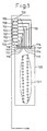
- Figure 2 shows an external view of a liquid crystal driving integrated circuit 101 according to one embodiment of the present invention.
- the integrated circuit chip containing the integrated circuit 101 is substantially rectangular in shape, having shorter and longer sides.
- a VDD input terminal 102 is a high voltage supply terminal
- a VSS input terminal 103 is a low voltage supply terminal
- a VM input terminal 130 is an intermediate voltage supply terminal.
- a signal A terminal 104 is an input terminal for inputting a signal A; a signal B terminal 105 is an input terminal for inputting a signal B; a signal C terminal 106 is an input terminal for inputting a signal C; a signal D terminal 107 is an input terminal for inputting a signal D; and a signal E terminal 108 is an input terminal for inputting a signal E.
- the signal input terminals are located inward of the power supply terminals. Input terminals for those signals for which the effect of the lead conductor resistance needs to be reduced are located close to an input edge 122.
- a VDD input terminal 112 like the VDD input terminal 102, is a high voltage supply terminal; a VSS input terminal 113, like the VSS input terminal 103, is a low voltage supply terminal; and a VM input terminal 131, like the VM input terminal 130, is an intermediate voltage supply terminal.
- a signal A terminal 114 is an input terminal for inputting the signal A; a signal B terminal 115, like the signal B terminal 105, is an input terminal for inputting the signal B; a signal C terminal 116, like the signal C terminal 106, is an input terminal for inputting the signal C; a signal D terminal 117, like the signal D terminal 107, is an input terminal for inputting the signal D; and a signal E terminal 118, like the signal E terminal 108, is an input terminal for inputting the signal E.
- the integrated circuit 101 is divided into two halves along a line 123 intersecting, at right angles, the longer sides of the substantially rectangular integrated circuit chip, and the terminals are arranged substantially symmetrical about the line 123.
- An output terminal array 120 consists of a plurality of output terminals arranged along an output edge 125.
- a VM terminal array 124 consists of a plurality of intermediate voltage supply terminals, and can be used to lower the input resistance in a structure where the FPC press-contact area is provided on the input edge 122 side.
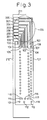
- Figure 3 shows a single-side lateral input type liquid crystal display substrate 211 having mounted thereon the liquid crystal driving integrated circuit 101 of the present invention shown in Figure 2 .
- an input electrode A 201 is an electrode for inputting a signal to the liquid crystal driving integrated circuit 101 via the input terminal A 104; an input electrode B 202 is an electrode for inputting a signal to the liquid crystal driving integrated circuit 101 via the input terminal B 105; an input electrode C 203 is an electrode for inputting a signal to the liquid crystal driving integrated circuit 101 via the input terminal C 106; an input electrode D 204 is an electrode for inputting a signal to the liquid crystal driving integrated circuit 101 via the input terminal D 107; and an input electrode E 205 is an electrode for inputting a signal to the liquid crystal driving integrated circuit 101 via the input terminal E 108.
- a VDD electrode 206 is an electrode for supplying power to the liquid crystal driving integrated circuit 101 via the VDD power supply terminal 102; a VSS electrode 207 is an electrode for supplying power to the liquid crystal driving integrated circuit 101 via the VSS terminal 103; and a VM electrode 208 is an electrode for supplying power to the liquid crystal driving integrated circuit 101 via the VM terminal 130.
- a press-contact area 224 provides a space for connecting the input electrodes to the FPC.
- the VM terminal 130 since the VM terminal 130 is located nearer to an input edge 212, the distance from the FPC becomes correspondingly shorter, reducing the resistance of the VM electrode 208.
- the input electrodes A 201 and B 202 are brought out of the liquid crystal driving integrated circuit 101 by being passed between the VM terminal 130 and the VDD terminal 102.
- the input electrodes C 203 and D 204 are brought out of the liquid crystal driving integrated circuit 101 by being passed between the VDD terminal 102 and the VSS terminal 103.
- the input electrode E 205 is brought out of the liquid crystal driving integrated circuit 101 by being passed alongside the VSS terminal 103.
- Figure 4 shows a liquid crystal display substrate 311 in an embodiment where the B signal, an input signal to the liquid crystal driving integrated circuit 101, is coupled to the VM power supply, the D signal is coupled to the VDD power supply, and the E signal is coupled to the VSS power supply.
- an input electrode A 301 is an electrode for inputting a signal to the liquid crystal driving integrated circuit 101 via the input terminal A 104
- an input electrode C 302 is an electrode for inputting a signal to the liquid crystal driving integrated circuit 101 via the input terminal C 106.
- the input electrode A 301 is brought out of the liquid crystal driving integrated circuit 101 by being passed between the VM terminal 130 and the VDD terminal 102.
- the input electrode C 302 is brought out of the liquid crystal driving integrated circuit 101 by being passed between the VDD terminal 102 and the VSS terminal 103.
- An input electrode B 303 is an electrode that connects the input terminal B 115 to the VM terminal 131
- an input electrode D 304 is an electrode that connects the input terminal D 117 to the VDD terminal 112
- an input electrode E 305 is an electrode that connects the input terminal E 118 to the VSS terminal 113.
- a VDD electrode 307 is an electrode for supplying power to the liquid crystal driving integrated circuit 101 via the VDD power supply terminal 102; a VSS electrode 308 is an electrode for supplying power to the liquid crystal driving integrated circuit 101 via the VSS terminal 103; and a VM electrode 309 is an electrode for supplying power to the liquid crystal driving integrated circuit 101 via the VM terminal 130.
- a press-contact area 324 provides a space for connecting the input electrodes to the FPC.
- the number of electrodes that must be brought out of a signal input area 320 is reduced to five, and the terminals to be set are located in a signal setting area 321. This arrangement serves to eliminate the problems associated with signal routing and permits the electrodes to be made thicker.
- Figure 5 shows a both-side lateral input type liquid crystal display substrate 411 having mounted thereon the liquid crystal driving integrated circuit 101 of the present invention shown in Figure 2 .
- an input electrode A 401 is an electrode for inputting a signal to the liquid crystal driving integrated circuit 101 via the input terminal A 114;
- an input electrode B 402 is an electrode for inputting a signal to the liquid crystal driving integrated circuit 101 via the input terminal B 105;
- an input electrode C 403 is an electrode for inputting a signal to the liquid crystal driving integrated circuit 101 via the input terminal C 116;
- an input electrode D 404 is an electrode for inputting a signal to the liquid crystal driving integrated circuit 101 via the input terminal D 107;
- an input electrode E 405 is an electrode for inputting a signal to the liquid crystal driving integrated circuit 101 via the input terminal E 118.
- a VDD electrode 406 is an electrode for supplying power to the liquid crystal driving integrated circuit 101 via the VDD power supply terminal 112; a VSS electrode 407 is an electrode for supplying power to the liquid crystal driving integrated circuit 101 via the VSS terminal 103; and a VM electrode 408 is an electrode for supplying power to the liquid crystal driving integrated circuit 101 via the VM terminal 130.
- a first press-contact area 424 and a second press-contact area 425 each provide a space for connecting the input electrodes to the FPC.
- the input electrode B 402 is brought out of the liquid crystal driving integrated circuit 101 by being passed between the VM terminal 130 and the VDD terminal 102, and the input electrode D 404 is brought out of the liquid crystal driving integrated circuit 101 by being passed between the VDD terminal 102 and the VSS terminal 103.
- the input electrode A 401 is brought out of the liquid crystal driving integrated circuit 101 by being passed alongside the VM terminal 131
- the input electrode C 403 is brought out of the liquid crystal driving integrated circuit 101 by being passed between the VDD terminal 112 and the VSS terminal 113
- the input electrode E 405 is brought out of the liquid crystal driving integrated circuit 101 by being passed alongside the VSS terminal 113.
- a VDD electrode 406 is an electrode for supplying power to the liquid crystal driving integrated circuit 101 via the VDD power supply terminal 112; a VSS electrode 407 is an electrode for supplying power to the liquid crystal driving integrated circuit 101 via the VSS terminal 103; and a VM electrode 408 is an electrode for supplying power to the liquid crystal driving integrated circuit 101 via the VM terminal 130.
- the number of electrodes that must be brought out of each of signal input areas 420 and 421 is as few as four since the electrodes are divided between the two sides. This arrangement serves to eliminate the problems associated with signal routing and permits the electrodes to be made thicker.
- Figure 6 shows a common input type liquid crystal display substrate 511 having mounted thereon the liquid crystal driving integrated circuit 101 of the present invention shown in Figure 2 .
- an input electrode A 501 is an electrode for inputting a signal to the liquid crystal driving integrated circuit 101 via the input terminal A 114;
- an input electrode B 502 is an electrode for inputting a signal to the liquid crystal driving integrated circuit 101 via the input terminal B 105;
- an input electrode C 503 is an electrode for inputting a signal to the liquid crystal driving integrated circuit 101 via the input terminal C 116;
- an input electrode D 504 is an electrode for inputting a signal to the liquid crystal driving integrated circuit 101 via the input terminal D 107;
- an input electrode E 505 is an electrode for inputting a signal to the liquid crystal driving integrated circuit 101 via the input terminal E 118.
- a VDD electrode 506 is an electrode for supplying power to the liquid crystal driving integrated circuit 101 via the VDD power supply terminal 112; a VSS electrode 507 is an electrode for supplying power to the liquid crystal driving integrated circuit 101 via the VSS terminal 103; and a VM electrode 508 is an electrode for supplying power to the liquid crystal driving integrated circuit 101 via the VM terminal array 124.
- a press-contact area 524 provides a space for connecting the input electrodes to the FPC.
- the VM electrode 508 is formed wide, the VM power is supplied to the integrated circuit 101 through a low resistance path.
- Figure 7 shows a lateral input type liquid crystal display substrate 611 having mounted thereon the liquid crystal driving integrated circuit 101 of the present invention shown in Figure 2 and a second liquid crystal driving integrated circuit 600, one connected in cascade with the other.
- an input electrode A 601 is an electrode for inputting a signal to the liquid crystal driving integrated circuit 101 via the input terminal A 104;
- an input electrode B 602 is an electrode for inputting a signal to the liquid crystal driving integrated circuit 101 via the input terminal B 105;
- an input electrode C 603 is an electrode for inputting a signal to the liquid crystal driving integrated circuit 101 via the input terminal C 106;
- an input electrode D 604 is an electrode for inputting a signal to the liquid crystal driving integrated circuit 101 via the input terminal D 107;
- an input electrode E 605 is an electrode for inputting a signal to the liquid crystal driving integrated circuit 101 via the input terminal E 108.
- a cascade electrode A 621 is an electrode that connects the signal A terminal 114 on the liquid crystal driving integrated circuit 101 to a signal A terminal 614 on the liquid crystal driving integrated circuit 600.
- a cascade electrode B 622 is an electrode that connects the signal B terminal 115 on the liquid crystal driving integrated circuit 101 to a signal B terminal 615 on the liquid crystal driving integrated circuit 600.
- a cascade electrode C 623 is an electrode that connects the signal C terminal 116 on the liquid crystal driving integrated circuit 101 to a signal C terminal 616 on the liquid crystal driving integrated circuit 600.
- a cascade electrode D 624 is an electrode that connects the signal D terminal 117 on the liquid crystal driving integrated circuit 101 to a signal D terminal 617 on the liquid crystal driving integrated circuit 600.
- a cascade electrode E 625 is an electrode that connects the signal E terminal 118 on the liquid crystal driving integrated circuit 101 to a signal E terminal 618 on the liquid crystal driving integrated circuit 600.
- a VDD electrode 607 is an electrode for supplying power to the liquid crystal driving integrated circuit 101 via the VDD power supply terminal 102; a VSS electrode 608 is an electrode for supplying power to the liquid crystal driving integrated circuit 101 via the VSS terminal 103; and a VM electrode 609 is an electrode for supplying power to the liquid crystal driving integrated circuit 101 via the VM terminal 130.
- a cascade VDD electrode 627 is an electrode that connects the VDD terminal 112 on the liquid crystal driving integrated circuit 101 to a VDD terminal 612 on the liquid crystal driving integrated circuit 600.
- a cascade VSS electrode 628 is an electrode that connects the VSS terminal 113 on the liquid crystal driving integrated circuit 101 to a VSS terminal 613 on the liquid crystal driving integrated circuit 600.
- a cascade VM electrode 629 is an electrode that connects the VM terminal 131 on the liquid crystal driving integrated circuit 101 to a VM terminal 631 on the liquid crystal driving integrated circuit 600.
- a press-contact area 624 provides a space for connecting the input electrodes to the FPC.
- Signal A is input to the liquid crystal driving integrated circuit 600 via the signal A electrode 601, the signal A terminal 104, a conductor within the liquid crystal driving integrated circuit 101, the signal A terminal 114, the cascade electrode A 621, and the signal A terminal 614.
- Signal B is input to the liquid crystal driving integrated circuit 600 via the signal B electrode 602, the signal B terminal 105, a conductor within the liquid crystal driving integrated circuit 101, the signal B terminal 115, the cascade electrode B 622, and the signal B terminal 615.
- Signal C is input to the liquid crystal driving integrated circuit 600 via the signal C electrode 603, the signal C terminal 106, a conductor within the liquid crystal driving integrated circuit 101, the signal C terminal 116, the cascade electrode C 623, and the signal C terminal 616.
- Signal D is input to the liquid crystal driving integrated circuit 600 via the signal D electrode 604, the signal D terminal 107, a conductor within the liquid crystal driving integrated circuit 101, the signal D terminal 117, the cascade electrode D 624, and the signal D terminal 617.
- Signal E is input to the liquid crystal driving integrated circuit 600 via the signal E electrode 605, the signal E terminal 108, a conductor within the liquid crystal driving integrated circuit 101, the signal E terminal 118, the cascade electrode E 625, and the signal E terminal 618.
- VDD power is input to the liquid crystal driving integrated circuit 600 via the VDD electrode 607, the VDD terminal 102, a conductor within the liquid crystal driving integrated circuit 101, the VDD terminal 112, the cascade VDD electrode 627, and the VDD input terminal 612.
- VSS power is input to the liquid crystal driving integrated circuit 600 via the VSS electrode 608, the VSS terminal 103, a conductor within the liquid crystal driving integrated circuit 101, the VSS terminal 113, the cascade VSS electrode 628, and the VSS terminal 613.
- VM power is input to the liquid crystal driving integrated circuit 600 via the VM electrode 609, the VM terminal 130, a conductor within the liquid crystal driving integrated circuit 101, the VM terminal 131, the cascade VM electrode 629, and the VM input terminal 631.
- liquid crystal driving integrated circuit 101 by supplying inputs laterally to one side of the liquid crystal driving integrated circuit 101, more than one liquid crystal driving integrated circuit can be driven.
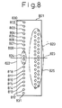
- FIG. 8 shows an external view of a liquid crystal driving integrated circuit 801 according to another embodiment of the present invention.
- the input terminals are arranged along a longer side of a substantially rectangular integrated circuit chip.
- a VDD terminal 802 is a high voltage supply terminal
- a VSS terminal 803 is a low voltage supply terminal
- a VM terminal 830 is an intermediate voltage supply terminal.
- a signal A terminal 804 is an input terminal for inputting a signal A; a signal B terminal 805 is an input terminal for inputting a signal B; a signal C terminal 806 is an input terminal for inputting a signal C; a signal D terminal 807 is an input terminal for inputting a signal D; and a signal E terminal 808 is an input terminal for inputting a signal E.
- the signal input terminals are located inward of the power supply terminals, and input terminals for those signals for which the effect of the lead conductor resistance needs to be reduced are located close to the shorter sides of the liquid crystal driving integrated circuit 801.
- a VDD terminal 812 like the VDD terminal 802, is a high voltage supply terminal; a VSS terminal 813, like the VSS terminal 803, is a low voltage supply terminal; and a VM terminal 831, like the VM terminal 830, is an intermediate voltage supply terminal.
- a signal A terminal 814 is an input terminal for inputting the signal A; a signal B terminal 815, like the signal B terminal 805, is an input terminal for inputting the signal B; a signal C terminal 816, like the signal C terminal 806, is an input terminal for inputting the signal C; a signal D terminal 817, like the signal D terminal 807, is an input terminal for inputting the signal D; and a signal E terminal 818, like the signal E terminal 808, is an input terminal for inputting the signal E.
- the integrated circuit 801 is divided into two halves along a line 823 intersecting at right angles with the longer sides of the substantially rectangular integrated circuit chip, and the terminals are arranged substantially symmetrical about the line 823.
- An output terminal array 820 consists of a plurality of output terminals arranged along an output edge 825.
- a VM terminal array 824 consists of a plurality of intermediate voltage supply terminals, and can be used to lower the input resistance in a structure where the FPC press-contact area is provided on the input edge 822 side.
- Figure 9 shows an embodiment where the B signal, an input signal to the liquid crystal driving integrated circuit 801, is coupled to the VM power supply and the E signal is coupled to the VSS power supply.
- an input electrode A 901 is an electrode for inputting a signal to the liquid crystal driving integrated circuit 801 via the input terminal A 804, and an input electrode C 902 is an electrode for inputting a signal to the liquid crystal driving integrated circuit 801 via the input terminal C 806.
- the input electrode A 901 is connected to the signal A terminal 804 by being passed through a press-contact area 924 and over the shorter side of the liquid crystal driving integrated circuit 801.
- the input electrode C 902 is connected to the signal C terminal 806 by being passed through the press-contact area 924 and over the shorter side of the liquid crystal driving integrated circuit 801.
- An input electrode B 903 is an electrode that connects the input terminal B 805 to the VM terminal array 824.
- An input electrode D 804 is an electrode that connects the input terminal D 817 to the VDD terminal 812.
- An input electrode E 905 is an electrode that connects the input terminal E 818 to the VSS terminal 813.
- a VDD electrode 907 is an electrode for supplying power to the liquid crystal driving integrated circuit 801 via the VDD power supply terminal 802.
- a VSS electrode 908 is an electrode for supplying power to the liquid crystal driving integrated circuit 801 via the VSS power supply terminal 803.
- a VM electrode 909 is an electrode for supplying power to the liquid crystal driving integrated circuit 801 via the VM terminal 830.
- a press-contact area 924 provides a space for connecting the input electrodes to the FPC.
- the number of electrodes that must be brought out of the press-contact area 924 serving as a signal input area is reduced to five, and the terminals for connection are located in a signal setting area 921.
- This arrangement serves to eliminate the problems associated with signal routing and permits the electrodes to be made thicker.
- the integrated circuit 801 is also applicable to any one of the first to sixth embodiments of the integrated circuit 101.
Landscapes
- Physics & Mathematics (AREA)
- Nonlinear Science (AREA)
- Mathematical Physics (AREA)
- Chemical & Material Sciences (AREA)
- Crystallography & Structural Chemistry (AREA)
- General Physics & Mathematics (AREA)
- Optics & Photonics (AREA)
- Liquid Crystal (AREA)
- Devices For Indicating Variable Information By Combining Individual Elements (AREA)
Abstract
Claims (8)
- Un substrat d'affichage à cristaux liquides sur lequel un circuit intégré de contrôle à cristaux liquides (101 ; 801) est monté directement, dans lequel le circuit intégré comprend une pluralité de rangées à bornes d'alimentation en énergie, une puce électronique de circuit intégré sensiblement rectangulaire, contenant le circuit intégré, est divisée en deux moitiés suivant une ligne (123 ; 823) coupant, à angle droit, les côtés longs de ladite puce électronique, et une première rangée à bornes d'alimentation en énergie (102, 103, 130 ; 802, 803, 830) est prévue sur une première moitié de la puce électronique de circuit intégré et une deuxième rangée à bornes d'alimentation en énergie (112, 113, 131 ; 812, 813, 831) est prévue sur l'autre moitié de celle-ci, caractérisé en ce qu'une troisième rangée à bornes d'alimentation en énergie (124 ; 824) est prévue entre la première rangée à bornes d'alimentation en énergie et la deuxième rangée à bornes d'alimentation en énergie, et les rangées à bornes sont connectées les unes aux autres.
- Le substrat d'affichage à cristaux liquides selon la revendication 1, caractérisé en ce qu'une première rangée à bornes d'entrée de signal (104 à 108 ; 804 à 808) est prévue sur une première moitié de la puce électronique de circuit intégré, et une deuxième rangée à bornes d'entrée de signal (114 à 118 ; 814 à 818) est prévue sur l'autre moitié de celle-ci, et les rangées à bornes sont connectées les unes aux autres.
- Le substrat d'affichage à cristaux liquides selon la revendication 1 ou 2, caractérisé en ce que les première et deuxième rangées à bornes d'alimentation en énergie comprennent chacune une borne d'entrée d'énergie à haute tension (102, 112; 802, 812), une borne d'entrée d'énergie à basse tension (103, 113 ; 803, 813) et une borne d'entrée d'énergie à tension intermédiaire (130, 131 ; 830, 831) et la troisième rangée à bornes d'alimentation en énergie (124 ; 824) comprend une borne d'entrée d'énergie à tension intermédiaire.
- Le substrat d'affichage à cristaux liquides selon la revendication 2, caractérisé en ce que les premières rangées à bornes sont agencées sur un côté court de la première moitié de puce électronique, la première rangée à bornes d'alimentation en énergie (102, 103, 130) étant située à l'extérieur de la première rangée à bornes d'entrée de signal (104, 105, 106, 107, 108), tandis que les deuxièmes rangées à bornes sont agencées le long d'un côté court de l'autre moitié de puce électronique, la deuxième rangée à bornes d'alimentation en énergie (112, 113, 131) étant située à l'extérieur de la deuxième rangée à bornes d'entrée de signal (114, 115, 116, 117, 118).
- Le substrat d'affichage à cristaux liquides selon la revendication 2, caractérisé en ce que la première rangée à bornes d'alimentation en énergie (102, 103, 130) et la première rangée à bornes d'entrée de signal (104, 106) sont connectées à des conducteurs électriques (301, 302, 307, 308, 309) introduits par un côté court de la première moitié de puce électronique, et la deuxième rangée à bornes d'entrée de signal (115, 117, 118) est connectée à la deuxième rangée à bornes d'alimentation en énergie (112, 113, 131).
- Le substrat d'affichage à cristaux liquides selon la revendication 2, caractérisé en ce que la première rangée à bornes d'alimentation en énergie et la première rangée à bornes d'entrée de signal) sont connectées à des conducteurs électriques introduits par un côté court de la première moitié de puce électronique, et la deuxième rangée à bornes d'entrée de signal (805) est connectée à la troisième rangée à bornes d'alimentation en énergie (824).
- Le substrat d'affichage à cristaux liquides selon la revendication 2, caractérisé en ce que certaines des bornes de la première rangée à bornes d'alimentation en énergie (103, 130) et de la première rangée à bornes d'entrée de signal (105, 107) sont connectées à des conducteurs électriques (402, 404, 407, 408) introduits par un côté court de la première moitié de puce électronique, tandis que les bornes d'alimentation en énergie (112) et les bornes d'entrée de signal (114, 116, 118) se trouvant dans les deuxièmes rangées à bornes, qui correspondent aux bornes d'alimentation en énergie et aux bornes d'entrée de signal se trouvant dans les premières rangées à bornes qui ne sont pas connectées aux conducteurs électriques introduits par un côté court de la première moitié de puce électronique, sont connectées à des conducteurs électriques (401, 403, 405, 406) introduits par un côté court de l'autre moitié de puce électronique.
- Le substrat d'affichage à cristaux liquides selon la revendication 1 ou 2, caractérisé en ce que la troisième rangée à bornes d'alimentation en énergie est connectée à des conducteurs électriques introduits par un côté plus long de la puce électronique de circuit intégré.
Applications Claiming Priority (3)
| Application Number | Priority Date | Filing Date | Title |
|---|---|---|---|
| JP28674397 | 1997-10-20 | ||
| JP28674397 | 1997-10-20 | ||
| PCT/JP1998/004740 WO1999021050A1 (fr) | 1997-10-20 | 1998-10-20 | Circuit integre assurant l'entrainement du cristal liquide |
Publications (3)
| Publication Number | Publication Date |
|---|---|
| EP0945752A1 EP0945752A1 (fr) | 1999-09-29 |
| EP0945752A4 EP0945752A4 (fr) | 2005-04-06 |
| EP0945752B1 true EP0945752B1 (fr) | 2011-02-23 |
Family
ID=17708463
Family Applications (1)
| Application Number | Title | Priority Date | Filing Date |
|---|---|---|---|
| EP98947955A Expired - Lifetime EP0945752B1 (fr) | 1997-10-20 | 1998-10-20 | Substrat d'affichage à cristal liquide à circuit de contrôle intégré monté directement |
Country Status (7)
| Country | Link |
|---|---|
| US (1) | US6329969B1 (fr) |
| EP (1) | EP0945752B1 (fr) |
| JP (1) | JP3838669B2 (fr) |
| CN (1) | CN1178093C (fr) |
| DE (1) | DE69842138D1 (fr) |
| TW (1) | TW505803B (fr) |
| WO (1) | WO1999021050A1 (fr) |
Families Citing this family (16)
| Publication number | Priority date | Publication date | Assignee | Title |
|---|---|---|---|---|
| US6744713B1 (en) * | 1998-06-15 | 2004-06-01 | Samsung Electronics Co., Ltd. | Recording medium for storing write protection information and write protection method thereof |
| KR100601598B1 (ko) * | 1998-06-15 | 2006-07-14 | 삼성전자주식회사 | 기록 방지 정보를 저장하는 기록 매체와 기록 방지 방법 |
| WO2002021199A1 (fr) * | 2000-09-08 | 2002-03-14 | Citizen Watch Co., Ltd. | Affichage a cristaux liquides |
| KR101022278B1 (ko) * | 2003-12-15 | 2011-03-21 | 삼성전자주식회사 | 구동 칩 및 이를 갖는 표시장치 |
| KR101051013B1 (ko) * | 2003-12-16 | 2011-07-21 | 삼성전자주식회사 | 구동 칩 및 이를 갖는 표시장치 |
| JP4920204B2 (ja) * | 2005-06-24 | 2012-04-18 | 富士電機株式会社 | 半導体装置 |
| TW200737109A (en) * | 2006-03-30 | 2007-10-01 | Au Optronics Corp | Display module |
| JP4198736B2 (ja) * | 2007-07-26 | 2008-12-17 | 三菱電機株式会社 | ソース線駆動回路及びそのソース線駆動回路を備えた表示装置 |
| JP4874209B2 (ja) * | 2007-10-11 | 2012-02-15 | 京セラ株式会社 | 液晶表示装置 |
| TWI373107B (en) * | 2008-04-24 | 2012-09-21 | Hannstar Display Corp | Chip having a driving integrated circuit and liquid crystal display having the same |
| US8299631B2 (en) * | 2008-09-01 | 2012-10-30 | Sharp Kabushiki Kaisha | Semiconductor element and display device provided with the same |
| WO2012176402A1 (fr) * | 2011-06-21 | 2012-12-27 | 株式会社村田製作所 | Module de circuit |
| JP5655845B2 (ja) * | 2012-11-13 | 2015-01-21 | 三菱電機株式会社 | 表示装置およびic |
| CN110610657A (zh) * | 2018-06-14 | 2019-12-24 | 格科微电子(上海)有限公司 | 用于便携式电子装置的显示面板的驱动芯片设计方法 |
| CN110221462B (zh) * | 2019-06-19 | 2024-05-17 | 深圳天德钰科技股份有限公司 | 显示面板、驱动器及软性电路板 |
| CN111679467A (zh) * | 2020-06-29 | 2020-09-18 | 武汉华星光电技术有限公司 | 显示面板及显示装置 |
Family Cites Families (8)
| Publication number | Priority date | Publication date | Assignee | Title |
|---|---|---|---|---|
| GB2166899B (en) * | 1984-11-09 | 1987-12-16 | Hitachi Ltd | Liquid crystal display device |
| JPH02166492A (ja) * | 1988-12-20 | 1990-06-27 | Fujitsu Ltd | ディスプレイパネル |
| JP2863363B2 (ja) * | 1992-01-24 | 1999-03-03 | シャープ株式会社 | 表示装置 |
| JP2994163B2 (ja) * | 1993-01-28 | 1999-12-27 | シャープ株式会社 | 平面型表示装置 |
| TW340192B (en) * | 1993-12-07 | 1998-09-11 | Sharp Kk | A display board having wiring with three-layered structure and a display device including the display board |
| JP3556315B2 (ja) * | 1995-03-20 | 2004-08-18 | 株式会社東芝 | 表示装置及び半導体素子 |
| JPH09101496A (ja) * | 1995-10-04 | 1997-04-15 | Sharp Corp | 表示装置駆動用電圧発生装置 |
| JP3541625B2 (ja) * | 1997-07-02 | 2004-07-14 | セイコーエプソン株式会社 | 表示装置及びアクティブマトリクス基板 |
-
1998
- 1998-10-20 WO PCT/JP1998/004740 patent/WO1999021050A1/fr active Application Filing
- 1998-10-20 DE DE69842138T patent/DE69842138D1/de not_active Expired - Lifetime
- 1998-10-20 JP JP52152299A patent/JP3838669B2/ja not_active Expired - Fee Related
- 1998-10-20 US US09/319,593 patent/US6329969B1/en not_active Expired - Lifetime
- 1998-10-20 EP EP98947955A patent/EP0945752B1/fr not_active Expired - Lifetime
- 1998-10-20 CN CNB988015501A patent/CN1178093C/zh not_active Expired - Fee Related
- 1998-10-20 TW TW087117311A patent/TW505803B/zh not_active IP Right Cessation
Also Published As
| Publication number | Publication date |
|---|---|
| WO1999021050A1 (fr) | 1999-04-29 |
| JP3838669B2 (ja) | 2006-10-25 |
| US6329969B1 (en) | 2001-12-11 |
| EP0945752A4 (fr) | 2005-04-06 |
| EP0945752A1 (fr) | 1999-09-29 |
| DE69842138D1 (de) | 2011-04-07 |
| TW505803B (en) | 2002-10-11 |
| CN1178093C (zh) | 2004-12-01 |
| CN1242840A (zh) | 2000-01-26 |
Similar Documents
| Publication | Publication Date | Title |
|---|---|---|
| EP0945752B1 (fr) | Substrat d'affichage à cristal liquide à circuit de contrôle intégré monté directement | |
| US5585666A (en) | Semiconductor device with chip layout having inner electrode configuration and liquid crystal display apparatus employing the semiconductor device | |
| US6839046B1 (en) | Display driving device and manufacturing method thereof and liquid crystal module employing the same | |
| EP0617311B1 (fr) | Dispositif d'affichage à cristal liquide | |
| US6344754B1 (en) | Semiconductor chip, semiconductor device package, probe card and package testing method | |
| US4142226A (en) | Multi-contact electrical edge connector for display panels | |
| JP2001188517A5 (fr) | ||
| KR930005378B1 (ko) | 액정표시용 집적회로 및 액정표시장치 | |
| US6459417B1 (en) | Display driving device and liquid crystal module using the same | |
| US6707440B2 (en) | Semiconductor device | |
| JPH05249927A (ja) | 駆動回路 | |
| US20020171638A1 (en) | Electrode driving apparatus and electronic equipment | |
| EP0369405A2 (fr) | Circuit intégré d'attaque de bus et circuit d'inversion rythmé | |
| US6731365B2 (en) | Array circuit of a liquid crystal display wherein common electrodes isolated each other in different pixel regions | |
| KR100368699B1 (ko) | 반도체장치 | |
| JP3235893B2 (ja) | 液晶表示装置の駆動回路 | |
| CN114550635B (zh) | 显示面板 | |
| US6303875B1 (en) | IC packages replaceable by IC packages having a smaller pin count and circuit device using the same | |
| US5401988A (en) | Standard cell layout arrangement for an LSI circuit | |
| KR100474056B1 (ko) | 회로기판 및 평면표시장치 | |
| US6759732B1 (en) | Semiconductor device with circuit cell array and arrangement on a semiconductor chip | |
| JP3071622B2 (ja) | 表示装置およびその駆動方法およびその実装方法 | |
| US6104366A (en) | Driving device for liquid crystal display with a high yield | |
| JPH04336812A (ja) | デジタル回路装置 | |
| JP3286513B2 (ja) | 表示装置 |
Legal Events
| Date | Code | Title | Description |
|---|---|---|---|
| PUAI | Public reference made under article 153(3) epc to a published international application that has entered the european phase |
Free format text: ORIGINAL CODE: 0009012 |
|
| 17P | Request for examination filed |
Effective date: 19990609 |
|
| AK | Designated contracting states |
Kind code of ref document: A1 Designated state(s): DE FR GB |
|
| RAP1 | Party data changed (applicant data changed or rights of an application transferred) |
Owner name: CITIZEN WATCH CO. LTD. |
|
| A4 | Supplementary search report drawn up and despatched |
Effective date: 20050218 |
|
| RIC1 | Information provided on ipc code assigned before grant |
Ipc: 7G 02F 1/13 B Ipc: 7G 02F 1/1345 B Ipc: 7G 02F 1/1333 A |
|
| 17Q | First examination report despatched |
Effective date: 20050428 |
|
| REG | Reference to a national code |
Ref country code: HK Ref legal event code: WD Ref document number: 1021233 Country of ref document: HK |
|
| RAP1 | Party data changed (applicant data changed or rights of an application transferred) |
Owner name: CITIZEN HOLDINGS CO., LTD. |
|
| RTI1 | Title (correction) |
Free format text: LIQUID CRYSTAL DISPLAY SUBSTRATE WITH DIRECTLY MOUNTED INTEGRATED CIRCUIT FOR DRIVING |
|
| GRAP | Despatch of communication of intention to grant a patent |
Free format text: ORIGINAL CODE: EPIDOSNIGR1 |
|
| GRAS | Grant fee paid |
Free format text: ORIGINAL CODE: EPIDOSNIGR3 |
|
| GRAA | (expected) grant |
Free format text: ORIGINAL CODE: 0009210 |
|
| AK | Designated contracting states |
Kind code of ref document: B1 Designated state(s): DE FR GB |
|
| REG | Reference to a national code |
Ref country code: GB Ref legal event code: FG4D |
|
| REF | Corresponds to: |
Ref document number: 69842138 Country of ref document: DE Date of ref document: 20110407 Kind code of ref document: P |
|
| REG | Reference to a national code |
Ref country code: DE Ref legal event code: R096 Ref document number: 69842138 Country of ref document: DE Effective date: 20110407 |
|
| PLBE | No opposition filed within time limit |
Free format text: ORIGINAL CODE: 0009261 |
|
| STAA | Information on the status of an ep patent application or granted ep patent |
Free format text: STATUS: NO OPPOSITION FILED WITHIN TIME LIMIT |
|
| 26N | No opposition filed |
Effective date: 20111124 |
|
| REG | Reference to a national code |
Ref country code: DE Ref legal event code: R097 Ref document number: 69842138 Country of ref document: DE Effective date: 20111124 |
|
| REG | Reference to a national code |
Ref country code: DE Ref legal event code: R084 Ref document number: 69842138 Country of ref document: DE Effective date: 20120814 |
|
| PGFP | Annual fee paid to national office [announced via postgrant information from national office to epo] |
Ref country code: FR Payment date: 20121018 Year of fee payment: 15 |
|
| REG | Reference to a national code |
Ref country code: FR Ref legal event code: ST Effective date: 20140630 |
|
| PG25 | Lapsed in a contracting state [announced via postgrant information from national office to epo] |
Ref country code: FR Free format text: LAPSE BECAUSE OF NON-PAYMENT OF DUE FEES Effective date: 20131031 |
|
| REG | Reference to a national code |
Ref country code: GB Ref legal event code: 746 Effective date: 20140814 |
|
| PGFP | Annual fee paid to national office [announced via postgrant information from national office to epo] |
Ref country code: GB Payment date: 20141015 Year of fee payment: 17 Ref country code: DE Payment date: 20141014 Year of fee payment: 17 |
|
| REG | Reference to a national code |
Ref country code: DE Ref legal event code: R119 Ref document number: 69842138 Country of ref document: DE |
|
| GBPC | Gb: european patent ceased through non-payment of renewal fee |
Effective date: 20151020 |
|
| PG25 | Lapsed in a contracting state [announced via postgrant information from national office to epo] |
Ref country code: DE Free format text: LAPSE BECAUSE OF NON-PAYMENT OF DUE FEES Effective date: 20160503 Ref country code: GB Free format text: LAPSE BECAUSE OF NON-PAYMENT OF DUE FEES Effective date: 20151020 |