EP0942594A2 - Festkörperbildaufnahmevorrichtung - Google Patents
Festkörperbildaufnahmevorrichtung Download PDFInfo
- Publication number
- EP0942594A2 EP0942594A2 EP99301833A EP99301833A EP0942594A2 EP 0942594 A2 EP0942594 A2 EP 0942594A2 EP 99301833 A EP99301833 A EP 99301833A EP 99301833 A EP99301833 A EP 99301833A EP 0942594 A2 EP0942594 A2 EP 0942594A2
- Authority
- EP
- European Patent Office
- Prior art keywords
- photoelectric conversion
- image sensor
- memory
- conversion elements
- block
- Prior art date
- Legal status (The legal status is an assumption and is not a legal conclusion. Google has not performed a legal analysis and makes no representation as to the accuracy of the status listed.)
- Granted
Links
Images


Classifications
-
- H—ELECTRICITY
- H10—SEMICONDUCTOR DEVICES; ELECTRIC SOLID-STATE DEVICES NOT OTHERWISE PROVIDED FOR
- H10F—INORGANIC SEMICONDUCTOR DEVICES SENSITIVE TO INFRARED RADIATION, LIGHT, ELECTROMAGNETIC RADIATION OF SHORTER WAVELENGTH OR CORPUSCULAR RADIATION
- H10F39/00—Integrated devices, or assemblies of multiple devices, comprising at least one element covered by group H10F30/00, e.g. radiation detectors comprising photodiode arrays
- H10F39/10—Integrated devices
- H10F39/12—Image sensors
-
- H—ELECTRICITY
- H04—ELECTRIC COMMUNICATION TECHNIQUE
- H04N—PICTORIAL COMMUNICATION, e.g. TELEVISION
- H04N25/00—Circuitry of solid-state image sensors [SSIS]; Control thereof
- H04N25/70—SSIS architectures; Circuits associated therewith
- H04N25/76—Addressed sensors, e.g. MOS or CMOS sensors
Definitions
- the present invention relates to an image sensor which has a memory together with photoelectric conversion elements within an identical semiconductor chip.
- Fig. 1 shows a one-dimensional image sensor.
- numeral 1 denotes a photoelectric conversion pixel composed of a bipolar transistor 2 and a MOS transistor 3 for resetting the base of the transistor 2.
- a PN junction formed in the base-collection junction region of the transistor 2 is irradiated, and a signal voltage generated by accumulation of electric charges owing to the incident light and the corresponding increase of base potential is output from the emitter of the transistor 2.
- the plurality of pixels 1 are arranged over one line.
- Numeral 50 denotes a voltage supply source for resetting the base of the pixel 1
- numeral 4 denotes a pixel output line connected to the emitter of the transistor 2
- numeral 5 denotes a MOS transistor for resetting the line 4
- numeral 6 denotes a bipolar transistor the base of which is connected to the line 4.
- the emitter of each transistor 6 in each line is connected to an output line 7 in common.
- the transistor 6 acts as a means for detecting the maximum value of the photoelectric conversion output, whereby the voltage corresponding to the maximum output voltage of the pixel array is generated from the output line 7.
- Numeral 8 denotes a storage capacitor for storing the output voltage of the pixel
- numeral 9 denotes a switching MOS transistor for performing connection and disconnection between the pixel output line 4 and the capacitor 8
- numeral 10 denotes a MOS transistor switch for selecting the capacitor 8
- numeral 11 denotes a shift register for outputting the control signal to the gate of the switch 10 to sequentially select the plurality of switches 10
- numeral 12 denotes an output line for reading the charges from the selected capacitor 8
- numeral 13 denotes an amplifier to which the line 12 is input
- numeral 14 denotes an output terminal of the amplifier 13
- numeral 15 denotes a comparator for judging the magnitude of the output value from the line 7
- numeral 16 denotes a driving control circuit for driving the photoelectric conversion block and also controlling the signal from the comparator 15
- numeral 17 denotes a driving line for, e.g., a clock signal, an inverted clock signal and a start signal to drive the shift register 11.
- Numerals 18, 19 and 20 denote driving lines respectively for applying gate driving pulses to the gates of MOS transistors 3, 5 and 9, numeral 21 denotes a wiring for supplying a comparison potential to the comparator 15, and numeral 22 denotes a latch circuit for latching the output of the comparator 15.
- the pixel 1, the capacitor 8 and the latch circuit 22 are simultaneously reset. After then, the switch 9 is set to be conductive as maintaining the level of the line 20 high. As the signal charges are accumulated in the pixel 1, the potentials of the line 4 and the capacitor 8 increase. Then, if the output corresponding to the maximum value of the pixel output exceeds the reference potential determined by the wiring 21, the output of the comparator 15 is inverted to switch over the latch circuit 22. Thus, since the level of the line 20 is changed to be low and also the switch 9 is turned off, the signals accumulated up to this time are held by the capacitor 8.
- the output values of the blocks can be at about the same level by controlling the pixel signal accumulation time of each block to be different.
- the pixel of bipolar type is shown by way of example in Fig. 1, generally a photoelectric conversion pixel of any type may be used.
- monitoring of the pixel output is not limited to the maximum value detection. Namely, the detector of minimum value or the detector difference between the maximum and minimum values may be designed.
- any problem does not occur in a case where the number of photoelectric conversion blocks is small and each block is formed at the position separated from others.
- the number of blocks is large and thus it is necessary to array the photoelectric conversion blocks closely, there is the problem that it is impossible to allocate the space on which the driving control circuit 16 and the shift register 11 are arranged.
- An object of the present invention is to downsize an image sensor.
- an image sensor comprising: a plurality of photoelectric conversion elements; and a memory for storing control information to control signals sent from the plurality of photoelectric conversion elements, wherein the plurality of photoelectric conversion elements and the memory are formed in an identical semiconductor chip.
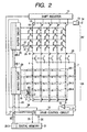
- numeral 1 denotes a photoelectric conversion pixel which is, like Fig. 1, composed of a reset MOS transistor and a bipolar transistor having a PN junction section of a photoelectric conversion element as its base.
- a pixel of other type such as MOS transistor amplification type pixel may be used.
- MOS transistor amplification type pixel may be used.
- Numeral 24 denotes a photoelectric conversion section in which four blocks 24-1, 24-2, 24-3 and 24-4 are formed.
- Numeral 25 denotes a drive line of the photoelectric conversion element, and
- numeral 26 denotes an analog memory cell corresponding to each photoelectric conversion pixel.
- the analog memory cell 26 is composed of a capacitor 8 acting as a memory and a switch 51, and is driven by a drive line 27 which is used to perform reading and writing of the memory by turning on/off the gate of the switch 51.
- the analog memory cells 26 the number of which is the same as that of the photoelectric conversion pixels 1 together form an analog memory section 26'.
- Numerals 28-1, 28-2 and 28-3 denote decoders through which the blocks are selected by address lines 32.
- Numeral 29 denotes a buffer circuit for selecting the driving line 25 in response to the output of the decoder 28-1
- numeral 30 denotes a buffer circuit for selecting the driving line 27 in response to the output of the decoder 28-2
- numeral 31 denotes a digital memory in which the control information for controlling the signal from the photoelectric conversion element has been written.
- the memory 31 is provided together with the photoelectric conversion section within one semiconductor chip, and is accessed in response to the output of the decoder 28-3.
- Numeral 33 denotes a wiring output from a driving control circuit 16 for driving the photoelectric conversion pixel blocks
- numeral 34 denotes a driving line also output from the circuit 16 for driving the analog memory blocks
- numeral 35 denotes a wiring for writing information into the digital memory 31
- numeral 36 denotes a wiring for reading the information stored in the memory 31.
- the photoelectric conversion section including the pixel 1 the analog memory section including the capacitor 8, and the digital memory section are all reset, and then the driving starts.
- the potential of the driving line 25 is set negative and a reset MOS transistor 3 is activated.
- the potential of the line 25 is set positive and the transistor 1 is activated, and simultaneously a MOS transistor 5 is turned on.
- the base current flows to reset the base of the transistor 1, and the line 25 is then returned to be ground level (GND), whereby the base-emitter junction at the transistor 1 becomes reversely biased.
- the switches 51 and 9 are turned on, whereby the potential at this section 8 is lowered to the ground potential through the MOS transistor 5.
- "1" or "0" is written at all memory bits.
- the address lines output from the driving control circuit 16 are changed over to repeatedly perform the reading of the photoelectric conversion blocks 24-1, 24-2, 24-3 and 24-4 in due order. In this operation, when each block is selected, the information of the digital memory 31 is also accessed.
- a comparator 51 is inverted by the output of, e.g., the block 24-2, i.e., if any one of the photoelectric conversion pixel output within the block 24-2 exceeds a threshold value obtained from a wiring 21, a pulse for writing into the block corresponding to the block 24-2 is applied to the wiring 34. Then, a pulse for turning on the transistor 51 in the corresponding line is output from the buffer circuit 30, whereby the signal of the block 24-2 is stored in the analog memory section 26'. Simultaneously, the information representing the signal transfer, the signal accumulation time of this block and the like is written at the address corresponding to the block 24-2 in the memory 31.
- the signal accumulation time represents the period of time from the accumulation start until the maximum photoelectric conversion signal in the block exceeds the threshold value.
- the driving control circuit 16 controls the driving lines 20 and 17 to turn off the switch 9. Also, the circuit 16 reads the output from the analog memory section by scanning the decoder 28-2 and causing the shift register 11.
- the signal accumulation time information recorded in the digital memory 31 is used in a signal process such as auto-focusing or the like.
- the driving information, the accumulation time information for each block, and the information representing whether or not the signal transfer was performed are recorded or stored as the control information for the signals sent from the photoelectric conversion elements.
- a random access memory RAM
- the digital memory 31 capable of writing and reading the control information for each block in the photoelectric conversion section and the analog memory section, it becomes possible to independently drive and control the plurality of closely arranged photoelectric conversion blocks 24-1, 24-2, 24-3 and 24-4, with the common driving control circuit, the common monitor circuit (i.e., maximum value detection circuit in the present embodiment), the common shift register and the like.
- the common driving control circuit i.e., maximum value detection circuit in the present embodiment
- the common shift register i.e., maximum value detection circuit in the present embodiment
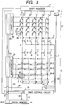
- Fig. 3 the difference from the first embodiment shown in Fig. 2 is as follows. That is, Fig. 2 shows that only the maximum value detection circuit for outputting the maximum photoelectric conversion charge in the block is provided, while Fig 3 shows that a minimum value detection circuit composed of parts 6' and 7' for outputting the minimum photoelectric conversion charge in the block is provided in addition to the maximum value detection circuit. Furthermore, in Fig. 3, the outputs from the maximum value detection circuit and the minimum value detection circuit are input to a different amplifier 45, and the gain of an amplifier 13 is controlled by a driving control circuit 16. Other points of the second embodiment are the same as those of the first embodiment shown in Fig. 2, whereby the explanations thereof are omitted.
- the operation to be performed until "1" or "0" is written at all the bits in the digital memory is the same as that in the first embodiment.
- the address lines output from the driving control circuit 16 are changed over to perform the reading of photoelectric conversion blocks 24-1, 24-2, 24-3 and 24-4 in due order.
- the signal accumulation time has been previously determined such that the respective blocks are read in the identical accumulation time.
- the driving control circuit 16 sends a pulse to a driving line 20 to turn on a transistor 9. Furthermore, the circuit 16 controls buffer circuits 29 and 30 and decoders 28-1, 28-2 and 28-3, whereby the photoelectric conversion charges in the photoelectric conversion section are sequentially signal-transferred to the analog memory section in the unit of block.
- the maximum photoelectric conversion charge in the block is output from the maximum value detection circuit to an output line 7, while the minimum photoelectric conversion charge in the block is output from the minimum value detection circuit to the output line 7'.
- the differential value between the maximum and minimum photoelectric conversion charges in each block is output from the differential amplifier 45.
- the obtained differential value is converted into the information concerning the gain of the amplifier at the time when the analog memory section finally outputs the signal, and the obtained information is recorded or stored in the digital memory section.
- the gain of the amplifier is set larger when the differential value is smaller, while smaller when the differential value is larger. For example, in case four different gains of the amplifier are set, each of the gains can be designated by digital information of two bits.
- the driving information and the information concerning the gain of the amplifier for each block are recorded in the digital memory unit.
- a random access memory (RAM) is used as the digital memory in the present embodiment.
- the common driving control circuit i.e., maximum value detection circuit and minimum value detection circuit in the present embodiment
- the common monitor circuit i.e., maximum value detection circuit and minimum value detection circuit in the present embodiment
- Fig. 4 shows the third embodiment of the present invention.
- Fig. 4 shows the block arrangement in which each of the first and third lines in the photoelectric conversion element array is divided into the two photoelectric conversion blocks, i.e., blocks 24-1-1 and 24-1-2 in the first line and blocks 24-3-1 and 24-3-2 in the third line. Further, Fig. 4 shows an address line 39 for discriminating the divided block in the line, while the address line 32 for designating the line is the same as that shown in Figs. 2 and 3.
- numeral 40 denotes a switching MOS transistor for connecting a maximum value detection circuit 6 and an output line 7 to each other.
- the transistor 40 is turned on/off by output lines 41 from a driving control circuit 16.
- Two driving lines 42 and 43 are provided to each of the first and third lines in the analog memory section so that the analog memory section has the block arrangement corresponding to that of the photoelectric conversion section.
- a driving line 25 is provided to each line in the same manner. By using the line 25, a pixel 1 is driven from a decoder 28-1 through a buffer circuit 29.
- the analog memory section having a storage capacity 8 is so constructed that the storage capacity is controllable from a decoder 28-2 through a buffer circuit 30 by selectively using the driving line 42 or 43 according to the corresponding line-divided photoelectric conversion block.
- numeral 37 denotes a read-only memory (ROM) recording whether the line selected by address lines 32 is composed of one block or two blocks.
- ROM read-only memory
- An output 38 from the ROM 37 is determined to be low when the selected line is composed of one block, while high when the selected line is composed of two blocks. Therefore, in a case where the driving control circuit 16 indicates a line by the address lines 32, it is possible to easily know from the output 38 whether or not the block in the line is divided.
- the driving control circuit 16 can easily detect the maximum value of the photoelectric conversion charge from the maximum value detection circuit 6 for every two blocks in the line. Then, the detected level is output by the circuit 16 to the output line 7, and compared with a threshold value by a comparator 15, whereby it is possible to store the signal accumulation time in the digital memory 31. Also, it is possible to read the image signal from the analog memory section to an output line 12, and then output through an amplifier 13.
- the address lines 39 are input also to the buffer circuit 30 for the analog memory section. Thus, if there are two blocks in one line, it becomes possible to independently control each block.
- control information for the signal sent from the photoelectric conversion element the driving information the accumulation time information for each block, and the information representing whether or not the signal has been transferred are stored in the digital memory 31 of the memory section. Furthermore, the information for distinguishing the block arrangement pattern in each line is stored in the ROM 37.
- a random access memory (RAM) is used as the digital memory in the present embodiment.
- the monitor circuit is not limited to that described above. That is, the circuit capable of obtaining the characteristic information of the respective blocks may be used.
- an addition circuit for obtaining addition signals of the respective photoelectric conversion blocks may be used as the monitor circuit.
Landscapes
- Engineering & Computer Science (AREA)
- Multimedia (AREA)
- Signal Processing (AREA)
- Transforming Light Signals Into Electric Signals (AREA)
- Solid State Image Pick-Up Elements (AREA)
Applications Claiming Priority (2)
| Application Number | Priority Date | Filing Date | Title |
|---|---|---|---|
| JP06122998A JP3468405B2 (ja) | 1998-03-12 | 1998-03-12 | 固体撮像装置 |
| JP06122998 | 1998-03-12 |
Publications (3)
| Publication Number | Publication Date |
|---|---|
| EP0942594A2 true EP0942594A2 (de) | 1999-09-15 |
| EP0942594A3 EP0942594A3 (de) | 2000-09-13 |
| EP0942594B1 EP0942594B1 (de) | 2008-06-18 |
Family
ID=13165191
Family Applications (1)
| Application Number | Title | Priority Date | Filing Date |
|---|---|---|---|
| EP99301833A Expired - Lifetime EP0942594B1 (de) | 1998-03-12 | 1999-03-11 | Festkörperbildaufnahmevorrichtung |
Country Status (6)
| Country | Link |
|---|---|
| US (1) | US6903772B1 (de) |
| EP (1) | EP0942594B1 (de) |
| JP (1) | JP3468405B2 (de) |
| KR (1) | KR100323483B1 (de) |
| CN (1) | CN1202575C (de) |
| DE (1) | DE69938910D1 (de) |
Cited By (6)
| Publication number | Priority date | Publication date | Assignee | Title |
|---|---|---|---|---|
| EP1143521A1 (de) * | 2000-04-05 | 2001-10-10 | Omnivision Technologies Inc. | CMOS Bildsensor mit nichtflüchtigem Speicher |
| US6441482B1 (en) | 2000-04-11 | 2002-08-27 | Omnivision Technologies, Inc. | Biometric device with integrated CMOS image sensor |
| EP1378149A4 (de) * | 2001-03-19 | 2009-04-01 | Afp Imaging Corp | Sensir-charakterisierung in einem speicher |
| CN101964857A (zh) * | 2009-07-22 | 2011-02-02 | 威海华菱光电有限公司 | 图像读取装置 |
| US9232147B2 (en) | 2011-05-31 | 2016-01-05 | Olympus Corporation | Image pickup apparatus and image pickup method |
| WO2018128816A1 (en) * | 2017-01-04 | 2018-07-12 | Semiconductor Components Industries, Llc | Methods and apparatus for a power management unit |
Families Citing this family (11)
| Publication number | Priority date | Publication date | Assignee | Title |
|---|---|---|---|---|
| CA2329287A1 (en) | 2000-01-21 | 2001-07-21 | Symagery Microsystems Inc. | Host interface for imaging arrays |
| JP2002252338A (ja) * | 2000-12-18 | 2002-09-06 | Canon Inc | 撮像装置及び撮像システム |
| JP2004260787A (ja) * | 2002-09-09 | 2004-09-16 | Rohm Co Ltd | イメージセンサモジュール |
| US7189909B2 (en) * | 2004-11-23 | 2007-03-13 | Román Viñoly | Camera assembly for finger board instruments |
| US20090122148A1 (en) * | 2007-09-14 | 2009-05-14 | Fife Keith G | Disjoint light sensing arrangements and methods therefor |
| JP5219481B2 (ja) * | 2007-12-06 | 2013-06-26 | キヤノン株式会社 | 撮像装置 |
| JP5244644B2 (ja) | 2008-03-07 | 2013-07-24 | オリンパス株式会社 | 固体撮像装置及びその応用装置 |
| KR20100010065A (ko) * | 2008-07-22 | 2010-02-01 | (주)실리콘화일 | Mems 가속도 센서의 신호처리블록을 구비한 cmos이미지센서 및 그 제조방법 |
| JP5460465B2 (ja) | 2010-05-25 | 2014-04-02 | キヤノン株式会社 | 光電変換装置および撮像システム |
| WO2013005389A1 (ja) * | 2011-07-01 | 2013-01-10 | パナソニック株式会社 | 固体撮像装置、固体撮像装置の駆動方法および撮像装置 |
| EP3036771A4 (de) * | 2013-03-15 | 2018-01-03 | Theranos, Inc. | Femtowatt-detektoranordnung mit nichtvakuumrohr |
Family Cites Families (10)
| Publication number | Priority date | Publication date | Assignee | Title |
|---|---|---|---|---|
| USRE34309E (en) | 1984-12-26 | 1993-07-13 | Canon Kabushiki Kaisha | Image sensor device having plural photoelectric converting elements |
| FR2580133B1 (de) * | 1985-04-05 | 1988-06-24 | Thomson Csf | |
| US5182658A (en) * | 1988-07-27 | 1993-01-26 | Canon Kabushiki Kaisha | Image pickup apparatus for controlling accumulation time in photoelectric elements |
| US5288988A (en) | 1990-08-07 | 1994-02-22 | Canon Kabushiki Kaisha | Photoconversion device having reset control circuitry |
| JPH06339082A (ja) | 1993-05-28 | 1994-12-06 | Canon Inc | 光電変換装置 |
| EP0653881B1 (de) | 1993-11-17 | 2001-08-16 | Canon Kabushiki Kaisha | Festkörperbildaufnahmevorrichtung |
| JPH07333059A (ja) * | 1994-06-07 | 1995-12-22 | Nikon Corp | 測光装置 |
| US5442465A (en) * | 1994-08-31 | 1995-08-15 | Eastman Kodak Company | Apparatus and method for controlling a linear imaging device |
| US6509927B1 (en) | 1994-12-16 | 2003-01-21 | Hyundai Electronics America Inc. | Programmably addressable image sensor |
| DE69631356T2 (de) | 1995-08-02 | 2004-07-15 | Canon K.K. | Halbleiter-Bildaufnehmer mit gemeinsamer Ausgangsleistung |
-
1998
- 1998-03-12 JP JP06122998A patent/JP3468405B2/ja not_active Expired - Fee Related
-
1999
- 1999-03-09 US US09/264,720 patent/US6903772B1/en not_active Expired - Fee Related
- 1999-03-11 EP EP99301833A patent/EP0942594B1/de not_active Expired - Lifetime
- 1999-03-11 DE DE69938910T patent/DE69938910D1/de not_active Expired - Fee Related
- 1999-03-12 KR KR1019990008408A patent/KR100323483B1/ko not_active Expired - Fee Related
- 1999-03-12 CN CNB991058399A patent/CN1202575C/zh not_active Expired - Fee Related
Cited By (8)
| Publication number | Priority date | Publication date | Assignee | Title |
|---|---|---|---|---|
| EP1143521A1 (de) * | 2000-04-05 | 2001-10-10 | Omnivision Technologies Inc. | CMOS Bildsensor mit nichtflüchtigem Speicher |
| US6441482B1 (en) | 2000-04-11 | 2002-08-27 | Omnivision Technologies, Inc. | Biometric device with integrated CMOS image sensor |
| EP1378149A4 (de) * | 2001-03-19 | 2009-04-01 | Afp Imaging Corp | Sensir-charakterisierung in einem speicher |
| CN101964857A (zh) * | 2009-07-22 | 2011-02-02 | 威海华菱光电有限公司 | 图像读取装置 |
| US9232147B2 (en) | 2011-05-31 | 2016-01-05 | Olympus Corporation | Image pickup apparatus and image pickup method |
| WO2018128816A1 (en) * | 2017-01-04 | 2018-07-12 | Semiconductor Components Industries, Llc | Methods and apparatus for a power management unit |
| US10209761B2 (en) | 2017-01-04 | 2019-02-19 | Semiconductor Components Industries, Llc | Methods and apparatus for a power management unit |
| US10824220B2 (en) | 2017-01-04 | 2020-11-03 | Semiconductor Components Industries, Llc | Methods and apparatus for a power management unit |
Also Published As
| Publication number | Publication date |
|---|---|
| KR100323483B1 (ko) | 2002-02-07 |
| CN1232298A (zh) | 1999-10-20 |
| CN1202575C (zh) | 2005-05-18 |
| EP0942594A3 (de) | 2000-09-13 |
| JPH11261894A (ja) | 1999-09-24 |
| DE69938910D1 (de) | 2008-07-31 |
| JP3468405B2 (ja) | 2003-11-17 |
| US6903772B1 (en) | 2005-06-07 |
| KR19990077844A (ko) | 1999-10-25 |
| EP0942594B1 (de) | 2008-06-18 |
Similar Documents
| Publication | Publication Date | Title |
|---|---|---|
| US6903772B1 (en) | Image sensor | |
| US5345266A (en) | Matrix array image sensor chip | |
| JP4187502B2 (ja) | 画質を向上させたイメージセンサ | |
| US6352869B1 (en) | Active pixel image sensor with shared amplifier read-out | |
| US6043478A (en) | Active pixel sensor with shared readout structure | |
| US5861620A (en) | Photoelectric converting apparatus | |
| KR101143698B1 (ko) | 고체 촬상 장치 | |
| US6980243B2 (en) | Photoelectric conversion device providing advantageous readout of two-dimensional array of transistors | |
| US7081607B1 (en) | Solid state image pickup device and image pickup system | |
| US6410900B1 (en) | Solid-state image sensor and method of driving the same | |
| US5731578A (en) | Solid-state imaging apparatus | |
| EP1507406B1 (de) | Bildsensor mit aktiver Rücksetzung und wahlfreien Pixeln | |
| CN101263708B (zh) | 电路、图像传感器、数字摄像机和用于操作像素的方法 | |
| US6747700B1 (en) | Solid state image pickup apparatus having a plurality of split buses | |
| US6580455B1 (en) | High definition image sensor | |
| JPH1084505A (ja) | 能動画素センサおよびその選択信号を生成する方法 | |
| JP3444906B2 (ja) | 光電変換装置 | |
| US6313455B1 (en) | CMOS pixel cell for image display systems | |
| KR19990072919A (ko) | 고체촬상장치,그구동방법및카메라 | |
| US6947085B1 (en) | CMOS sensor with data flow control | |
| US20020097446A1 (en) | Apparatus and method for dark calibration of a linear CMOS sensor | |
| JP3862683B2 (ja) | 固体撮像装置 | |
| JP3053721B2 (ja) | 固体撮像装置 | |
| JP3149126B2 (ja) | 固体撮像装置 | |
| JPH11298797A (ja) | 画像検出装置 |
Legal Events
| Date | Code | Title | Description |
|---|---|---|---|
| PUAI | Public reference made under article 153(3) epc to a published international application that has entered the european phase |
Free format text: ORIGINAL CODE: 0009012 |
|
| AK | Designated contracting states |
Kind code of ref document: A2 Designated state(s): DE FR GB IT NL |
|
| AX | Request for extension of the european patent |
Free format text: AL;LT;LV;MK;RO;SI |
|
| PUAL | Search report despatched |
Free format text: ORIGINAL CODE: 0009013 |
|
| AK | Designated contracting states |
Kind code of ref document: A3 Designated state(s): AT BE CH CY DE DK ES FI FR GB GR IE IT LI LU MC NL PT SE |
|
| AX | Request for extension of the european patent |
Free format text: AL;LT;LV;MK;RO;SI |
|
| 17P | Request for examination filed |
Effective date: 20010129 |
|
| AKX | Designation fees paid |
Free format text: DE FR GB IT NL |
|
| 17Q | First examination report despatched |
Effective date: 20040113 |
|
| GRAP | Despatch of communication of intention to grant a patent |
Free format text: ORIGINAL CODE: EPIDOSNIGR1 |
|
| GRAS | Grant fee paid |
Free format text: ORIGINAL CODE: EPIDOSNIGR3 |
|
| GRAA | (expected) grant |
Free format text: ORIGINAL CODE: 0009210 |
|
| AK | Designated contracting states |
Kind code of ref document: B1 Designated state(s): DE FR GB IT NL |
|
| REG | Reference to a national code |
Ref country code: GB Ref legal event code: FG4D |
|
| REF | Corresponds to: |
Ref document number: 69938910 Country of ref document: DE Date of ref document: 20080731 Kind code of ref document: P |
|
| PG25 | Lapsed in a contracting state [announced via postgrant information from national office to epo] |
Ref country code: NL Free format text: LAPSE BECAUSE OF FAILURE TO SUBMIT A TRANSLATION OF THE DESCRIPTION OR TO PAY THE FEE WITHIN THE PRESCRIBED TIME-LIMIT Effective date: 20080618 |
|
| NLV1 | Nl: lapsed or annulled due to failure to fulfill the requirements of art. 29p and 29m of the patents act | ||
| PLBE | No opposition filed within time limit |
Free format text: ORIGINAL CODE: 0009261 |
|
| STAA | Information on the status of an ep patent application or granted ep patent |
Free format text: STATUS: NO OPPOSITION FILED WITHIN TIME LIMIT |
|
| 26N | No opposition filed |
Effective date: 20090319 |
|
| PG25 | Lapsed in a contracting state [announced via postgrant information from national office to epo] |
Ref country code: IT Free format text: LAPSE BECAUSE OF FAILURE TO SUBMIT A TRANSLATION OF THE DESCRIPTION OR TO PAY THE FEE WITHIN THE PRESCRIBED TIME-LIMIT Effective date: 20080618 |
|
| REG | Reference to a national code |
Ref country code: FR Ref legal event code: ST Effective date: 20091130 |
|
| PG25 | Lapsed in a contracting state [announced via postgrant information from national office to epo] |
Ref country code: DE Free format text: LAPSE BECAUSE OF NON-PAYMENT OF DUE FEES Effective date: 20091001 |
|
| PG25 | Lapsed in a contracting state [announced via postgrant information from national office to epo] |
Ref country code: FR Free format text: LAPSE BECAUSE OF NON-PAYMENT OF DUE FEES Effective date: 20091123 |
|
| PGFP | Annual fee paid to national office [announced via postgrant information from national office to epo] |
Ref country code: GB Payment date: 20140318 Year of fee payment: 16 |
|
| GBPC | Gb: european patent ceased through non-payment of renewal fee |
Effective date: 20150311 |
|
| PG25 | Lapsed in a contracting state [announced via postgrant information from national office to epo] |
Ref country code: GB Free format text: LAPSE BECAUSE OF NON-PAYMENT OF DUE FEES Effective date: 20150311 |