EP0933758B1 - Schaltung für optische Informationswiedergabevorrichtung, optisches Informationswiedergabevorrichtung und Verfahren zur Wiedergabe von Informationen - Google Patents
Schaltung für optische Informationswiedergabevorrichtung, optisches Informationswiedergabevorrichtung und Verfahren zur Wiedergabe von Informationen Download PDFInfo
- Publication number
- EP0933758B1 EP0933758B1 EP99300692A EP99300692A EP0933758B1 EP 0933758 B1 EP0933758 B1 EP 0933758B1 EP 99300692 A EP99300692 A EP 99300692A EP 99300692 A EP99300692 A EP 99300692A EP 0933758 B1 EP0933758 B1 EP 0933758B1
- Authority
- EP
- European Patent Office
- Prior art keywords
- identification information
- signal
- output
- information
- track
- Prior art date
- Legal status (The legal status is an assumption and is not a legal conclusion. Google has not performed a legal analysis and makes no representation as to the accuracy of the status listed.)
- Expired - Lifetime
Links
Images


Classifications
-
- G—PHYSICS
- G11—INFORMATION STORAGE
- G11B—INFORMATION STORAGE BASED ON RELATIVE MOVEMENT BETWEEN RECORD CARRIER AND TRANSDUCER
- G11B7/00—Recording or reproducing by optical means, e.g. recording using a thermal beam of optical radiation by modifying optical properties or the physical structure, reproducing using an optical beam at lower power by sensing optical properties; Record carriers therefor
- G11B7/004—Recording, reproducing or erasing methods; Read, write or erase circuits therefor
- G11B7/005—Reproducing
- G11B7/0053—Reproducing non-user data, e.g. wobbled address, prepits, BCA
-
- G—PHYSICS
- G11—INFORMATION STORAGE
- G11B—INFORMATION STORAGE BASED ON RELATIVE MOVEMENT BETWEEN RECORD CARRIER AND TRANSDUCER
- G11B7/00—Recording or reproducing by optical means, e.g. recording using a thermal beam of optical radiation by modifying optical properties or the physical structure, reproducing using an optical beam at lower power by sensing optical properties; Record carriers therefor
- G11B7/08—Disposition or mounting of heads or light sources relatively to record carriers
- G11B7/09—Disposition or mounting of heads or light sources relatively to record carriers with provision for moving the light beam or focus plane for the purpose of maintaining alignment of the light beam relative to the record carrier during transducing operation, e.g. to compensate for surface irregularities of the latter or for track following
- G11B7/0948—Disposition or mounting of heads or light sources relatively to record carriers with provision for moving the light beam or focus plane for the purpose of maintaining alignment of the light beam relative to the record carrier during transducing operation, e.g. to compensate for surface irregularities of the latter or for track following specially adapted for detection and avoidance or compensation of imperfections on the carrier, e.g. dust, scratches, dropouts
Definitions
- the present invention relates to an optical information reproduction device. More specifically, this invention relates to a device for optically reproducing information from a disk medium on which concentric or spiral tracks are disposed, the medium comprising identification information areas in which identification information representing address information and the like are shifted radially inward and radially outward each approximately by a predetermined distance with respect to a track center and user information areas in which user information and the like are recorded on the center of a track.
- a recording track is generally divided into sectors in the direction of the track, and in each of the sectors, identification information, such as a track number, and a sector number, is preformatted as physically formed convex and concave pits.
- the identification information is disposed in either of these methods: In one method, dedicated identification information for a land track or groove track is disposed; in another method, the information is disposed in a position shifted in a radial direction so that the information can be shared by a land track and a groove track adjacent to the land track, more specifically, along the boundary between a land track and a groove track.
- the former method in which exclusive identification information is disposed in each track enables track-specific information to be included, making it easy to control the device.
- the pit width needs to be sufficiently narrower than the track pitch. It is therefore difficult to form desired pits with the same laser beam as that used for forming guide grooves. Thus, disk production process is complicated.
- the device In the latter method of sharing identification information by a land track and a groove track adjacent to the land track, the device needs to judge which track is being reproduced because two tracks share the identification information, and the control is a little more complicated than that for the former exclusive disposition method.
- the same laser beam as that used for forming guide grooves can be used for pre-formatting the identification information in mastering, which can be done by deflecting the laser beam in a radial direction just by 1/4 of the distance between the centers of the adjacent lands, by the use of a light deflection means.
- This type of optical disk and an optical information reproduction device using such optical disks are disclosed in Japanese Patent Application Kokai Publication No. 176404/1994.
- FIG. 7 shows the track format of the conventional optical disk.
- Fig. 8 shows how the conventional identification information portion is disposed.
- Fig. 9 is a block diagram showing the configuration of the optical information reproduction device for reproducing information from that type of optical disk.
- reference numeral 1 denotes an identification information area in which identification information is preformatted
- reference numeral 2 denotes a user information area in which user information is recorded by means of a variation in the local optical constant or physical shape
- reference numeral 3 denotes a groove track
- reference numeral 4 denotes a land track.
- the groove track 3 or land track 4 is disposed in spiral form in the full circumferential extent, and the tracks are divided into sectors in the direction of the tracks.
- a sector includes, at the beginning, the identification information area 1 in which information for identifying the sector, such as the track number and sector number is recorded, and the identification information area 1 is followed by the user information area 2 for recording user data and the like.
- the identification information is shared by the land track 4 and the groove track 3 adjacent to the land track, and the displacement of the identification information from the track center of the land track 4 or groove track 3 is 1/4 of the distance between adjacent land tracks 4 or of adjacent groove tracks 3.
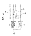
- reference numeral 11 denotes an optical disk
- reference numeral 12 denotes a spindle motor
- reference numeral 13 denotes an optical head
- reference numeral 14 denotes a first current-to-voltage (I/V) converting means
- reference numeral 15 denotes a second I/V converting means.
- An adding means 16 adds the output of the first I/V converting means 14 and the output of the second I/V converting means 15.
- a sum signal detecting means 17 detects the information recorded on the disk by processing and then converts the output (a) of the adding means 16 into binary values.
- a subtracting means 18 obtains a difference between the output of the first I/V converting means 14 and the output of the second I/V converting means 15.
- a polarity reversing means 19 reverses the polarity of the output waveform (b) of the subtracting means 18 according to the control signal from a controller 26, which will be described later.
- a difference signal detecting means 20 detects the information recorded on the disk by processing and then converts the output (d) of the polarity reversing means 19 into binary values.
- a signal selecting means 21 selects the output (c) of the sum signal detecting means 17 or the output (e) of the difference signal detecting means 20 according to the control signal (f) from a control gate generation means 25, which will be described later.
- a clock generation means 22 generates the reproduction clock (CK) in synchronization with the output (g) of the signal selecting means 21 according to a control gate signal (RG) from the control gate generation means 25.
- a data demodulating means 23 judges whether the output (g) of the signal selecting means 21 is at level “1" or "0" at the timing of the reproduction clock from the reproduction clock generation means 22 and demodulates the data.
- An address information reproduction means 24 reproduces an address after reproducing identification information by judging at the timing of the reproduction clock from the reproduction clock generation means 22 whether the output (g) of the signal selecting means 21 is at level "1" or "0".
- the control gate generation means 25 generates the control gate signal mentioned earlier, with reference to the timing of the address reproduction completion signal from the address information reproduction means 24.
- the controller 26 outputs a control signal to the polarity reversing means 19 according to the address information from the address information reproduction means 24.
- the optical head 13 comprises a laser diode (LD) 131, a collimate lens 132, a beam splitter (BS) 133, a converging lens 134, and a photodetector (PD) 135.
- LD laser diode
- BS beam splitter
- PD photodetector
- Fig. 10A to Fig. 10H show waveforms at various points in Fig. 9.
- the controller 26 sends a spindle activation signal and speed information, which are not shown, to a rotation controlling means, which is not shown, to adjust the spindle motor 12 to a predetermined speed. Then, the laser diode 131 of the optical head 13 is turned on by a lighting command, which is not shown, from the controller 26. The output of the laser diode 131 is kept to a constant value by a feedback controlling means, which is not shown.
- the collimate lens 132 converts the laser beam emitted from the laser diode 131 into parallel rays of light, which pass the beam splitter 133 and are converged onto the optical disk 11 by the converging lens 134. After passing the converging lens 134, the far field pattern of the light reflected from the optical disk 11 (return light), which includes the information component on the optical disk 11, is reflected by the beam splitter 133 and projected onto the photodetector 135.
- the photodetector 135 has at least two light-receiving parts which are disposed on opposite sides (radially outward and radially inward sides) of a track tangential line in the projected far-field pattern, i.e., of a track tangential line in the far field of the information pits on the optical disk 11.
- the optical system for passing the light beam from the laser diode 131 in the optical head 13 to the surface of the optical disk 11, and passing the light reflected at the surface of the optical disk 11 to the photodetector 135 is so designed that the center of the far field pattern of the information pits on the optical disk 11 is formed at the boundary between the two parts of the photodetector 135.
- the optical system of the optical head 13 is adjusted so that the position of the beam spot in the radial direction can be controlled through the use of the light distribution information on the two-part split photodetector 135.
- the beam spot When the beam spot is in the center of a track, identical amounts of light strike the two parts of the split photodetector 135, and the difference between the two outputs, that is a push-pull signal, is zero. As the beam spot goes away from the center of the track, the distribution of light on the two-part split photodetector becomes unbalanced, increasing the value of the push-pull signal.
- the value of the push-pull signal is zero when the beam spot is in the center of the land track 4 or groove track 3, and the value is maximized or minimized when the beam spot is on the boundary between the land track 4 and groove track 3.
- Tracking to keep the beam spot in the center of a track can be performed through feedback control to set the difference between the output signals from the two-part split photodetector 135 to zero. This technique is commonly utilized as a tracking method for optical disks having guide grooves.
- the light reflected from the optical disk 11 (return light) including the information component on the optical disk 11, which is mentioned above, is converted into current signals by the photodetector 135, which are then converted into voltage signals by the first I/V converting means 14 and the second I/V converting means 15 in the subsequent stage.
- a tracking error signal can be obtained in the push-pull method mentioned above.
- a tracking control means which is not shown, performs control so that the beam spot always scans the center of a track.
- a focus controlling means which is not shown, performs control to keep the beam spot converged onto the optical disk 11.
- the information on the optical disk 11 is read.
- Information is recorded onto the optical disk 11. The following description is limited to the reproduction of the information.
- the voltage signals from the first I/V converting means 14 and the second I/V converting means 15 are added by the adding means 16 to form a waveform as shown as (a) in Fig. 10A.
- the output from the subtracting means 18 mentioned above has a waveform as shown as (b) in Fig. 10C or (b') in Fig. 10D when the beam spot is at the center of a track. Whether the waveform is like (b) or (b') depends on whether the position of pits in the identification information area 1 is shifted radially inward or radially outward with respect to the center of the land track 4. Since the beam spot is at the center of the track in the user information area, the outputs from the two parts of the split photodetector 135 are the same, and the output of the subtracting means 18 is 0 (or a reference level).
- the light beam is scanning pits in the identification information area which are shifted radially inward with respect to the center of the land track. If the outputs from the two I/O converting means are connected to the subtracting means 18 in such a manner that the signal reproduced from the identification information area has the waveform as shown as (b) in Fig. 10C when the land track of the optical disk 11 is reproduced, the signal reproduced from the identification information area in the groove track reproduction has a waveform as shown as (b') in Fig. 10D. The reverse also holds.
- the analog signal output from the adding means 16 is judged to be larger or smaller than a predetermined slice level (Vth1) and is converted into binary values by the sum signal detecting means 17 and has a waveform as shown as (c) in Fig. 10B.
- the polarity of the reproduction waveform of the analog signal output from the subtracting means 18 differs depending on whether the reproduced track is a land track or a groove track, as described above.
- the level slicing means that produces binary values by slicing the analog waveform is designed with the polarity of input signal fixed.
- a system in which the polarity of the reproduced waveform changes therefore requires the polarity reversing means 19 to provide a signal of a fixed polarity.
- the polarity reversing means 19 can be easily controlled if the relationship between the track and the polarity of the reproduced waveform is known beforehand. That is, the controller 26, which will be described below, may operate the polarity reversing means 19 by judging whether the sector being scanned is on the land track or groove track. As a result, as shown as (d) in Fig. 10E, the polarity of the reproduced waveform of the identification information is maintained, irrespective of whether the sector being scanned is in the land track or groove track. In the shown example, the waveform is kept below the reference level.
- the output of the polarity reversing means 19 is converted into binary values by the difference signal detecting means 20, resulting in the waveform as shown as (e) shown in Fig. 10F.
- identification information such as a track address and sector address and the user information such as user data from binary signals
- user information includes data used for phase-locked loop pulling-in, synchronization pattern, error-detection and correction codes, as well as “user data”.
- the signal selecting means 21 is set to always select the output (c) of the sum signal detecting means 17.
- the signal selecting means 21 accordingly switches to select the desired signal.
- the switching of the signal selecting means 21 is made according to the switching signal (f) (shown in Fig. 10G) from the control gate generation means 25, which will be described later.
- the switching signal is generated by an internal timer or the like, which is started by a timing signal which can identify a known position within a sector, such as the address detection completion timing signal from the address information reproduction means 24.
- the output (g) of the signal selecting means 21 is supplied to the reproduction clock generation means 22, the data demodulating means 23, and the address information reproduction means 24.
- the reproduction clock generation means 22 generates the reproduction clock in synchronization with the output signal (g) from the signal selecting means 21, using a phase locked loop (PLL) means.
- the reproduction clock generation means 22 is designed to operate within the area in which the information to be reproduced is present, according to a read gate signal (RG) from the control gate generation means 25.
- the address information reproduction means 24 reproduces the identification information by checking at the timing of the reproduction clock from the reproduction clock generation means 22 whether the output signal (g) from the signal selecting means 21 is at "1" or "0", and thereby detects an address.
- the data demodulating means 23 demodulates data by checking at the timing of the reproduction clock from the reproduction clock generation means 22 whether the output signal (g) from the signal selecting means 21 is at "1" or "0" and then performs decoding, error correction, and deinterleaving.
- the control gate generation means 25 generates the switching signal (f) (shown in Fig. 3I) of the signal selecting means 21 and the read gate signal (RG) (shown in Fig. 3J, to be supplied to the reproduction clock generation means 22) according to the internal timer, started at the address detection completion timing (shown in Fig. 3H) provided by the address information reproduction means 24.
- the address detection completion timing is a timing when the decoding of the address having been read from the identification information area is completed. In the drawing, it is shown to be immediately after the end of the identification information area.
- the controller 26 identifies the sector from which information is being reproduced according to the address reproduced by the address information reproduction means 24 and the information indicating whether information is being reproduced from a land track or a groove track, which is obtained from the tracking control means. If the track from which information is to be reproduced is changed at an access or on other occasions, the controller judges whether the track containing the target sector is the land track or groove track and outputs a control signal for setting the polarity of the output signal to the polarity reversing means 19. In addition, the controller 26 controls the whole device, which is not shown.
- the identification information is disposed between a land track and a groove track, being shifted from a track center, the identification information can be reproduced and detected regardless of whether the beam spot is scanning a land track and a groove track. Because the identification information need not be separately formed for the land track and for the groove track, the number of processes in optical disk mastering can be reduced.
- identification information is shared by a land track and a groove track, as described above, it is hard to identify a sector just by reproducing the address, and the information indicating whether information is being reproduced from a land track or a groove track is additionally required.
- any track offset of the beam spot in a radial direction away from the identification information causes the amplitude of the signal reproduced from the identification information to be degraded, reducing the address detection accuracy.
- a low address detection accuracy will result in a low recording reliability or a low reproduction reliability.
- the scale of the circuit is large.
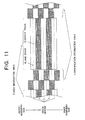
- an optical disk with the identification information disposed in a staggering manner as shown in Fig. 11 is provided.
- a feature of this disposition is that identification information is split into two areas and that the information of one area (hereafter referred to as the first identification information) is shifted by a predetermined distance radially outward with respect to the track center, and the information of the other area (hereafter referred to as the second identification information) is shifted by a predetermined distance radially inward with respect to the track center and radially inward with respect to the center of the track.
- the amount of shift is preferably about 1/2 of the track pitch.
- the tracking offset can be canceled. That is, when the first identification information and second identification information reproduced by the subtracting means mentioned above have the same reproduction amplitude, the beam spot is judged to be at the center of the track.
- the track on which the beam spot is scanning can be known. That is, when the beam spot is scanning a land track, the first identification information (shifted radially outward) is detected, and then the second identification information (shifted radially inward) is detected. When the beam spot is scanning a groove track, the second identification information (shifted radially inward) is detected, and then the first identification information (shifted radially outward) is detected.
- the conventional optical information reproduction device as described above with reference to Fig. 8, however, is designed on the assumption that the identification information is shifted in only one direction with respect to the track center, and the polarity reversing means can be controlled just in units of tracks, that is, the polarity is not switched until the end of each land track or each grove track. With this configuration, it is impossible to control the signal polarity for each piece of identification information. Accordingly, if the conventional optical information reproduction device is used to reproduce information from an optical disk as shown in Fig. 11, just the output of the adding means can be used to detect the identification information, and the push-pull signal output from the subtracting means cannot be used. In this case, the first identification information and second identification information cannot be separately detected, and whether the track from which information is reproduced is a land track or a groove track cannot be judged solely from the detected identification information.
- a judging means such as one which makes judgment by evaluating the accuracy or reliability of address detection, for deciding which of the outputs from the adding means and subtracting means is to be used for reproduction of the identification information is not available, and the address detection accuracy may therefore be degraded.
- EP-A-0 801.382 relates to an optical information recording and reproducing device and associated method adapted to record or reproduce information on a recording medium having an optical detector including two light receiving portions connected to means for generating a difference signal and means for generating an addition signal between the two portions and which includes means for differentiating between a header portion and a data portion by detecting an envelope of the difference signal.
- the present invention relates to an optical information reproduction device for reproducing information from an optical disk with identification information disposed in a staggering manner, and seeks to solve the problems of the conventional device as described above.
- a first object of the invention is to provide an optical information reproduction device for reproducing information from an optical disk having a first identification information area and a second identification information area in which identification information representing address information and the like are disposed, being shifted respectively radially outward and radially inward by a predetermined distance with respect to the track center and a user information area in which user information and the like are recorded on the center of a track.
- An eleventh object of the invention is to improve the probability of signal detection by separately setting offset value for the first and second identification information and user information of the land track and of the groove track on a disk medium.
- An optical information reproduction device is for reproducing information from an optical disk medium on which an identification information area including first identification information shifted radially outward with respect to the center of a recording track by a specified distance and second identification information shifted radially inward with respect to the center of a recording track by a specified distance, and a user information area disposed along the center of a recording track are disposed in concentric or spiral form, said optical information reproduction device comprising:
- a signal processing circuit is for used in an optical information reproduction device for reproducing information from an optical disk medium on which an identification information area including first identification information shifted radially outward with respect to the center of a recording track by a specified distance and second identification information shifted radially inward with respect to the center of a recording track by a specified distance, and a user information area disposed along the center of a recording track are disposed in concentric or spiral form, and including an optical head (13) illuminating the optical disk medium with a light beam, and including a split photodetector (135) having at least two light-receiving parts disposed on opposite side of a track tangential line in the far field of the optical disk medium and receiving light reflected from the optical disk medium, and comprises an adding means (16) for adding the outputs of said split photodetector (135); a subtracting means (18) which obtains a difference between the outputs of said split photodetector (135); a difference signal processing means (35) which makes
- the difference signal processing means (35) may comprise:
- the polarity switching signal generation means (353) may comprise:
- the waveform shaping means (37) may comprise:
- the signal slice means (375) may comprise:
- the slice level adjusting means (378) may be configured so that it can set the offset values separately for the first identification information, the second information, and the user information.
- the slice level adjustment means (378) may be configured to generate a second boost gate signal of a predetermined duration generated in accordance with the outputs of the first to fourth gate generation means, and reduces the time constant for control of the slice level, for the period of said second boost gate signal.
- the boost gate generation means (373) and the slice level adjustment means (378) may be configured so that they can set the period of the boost gate signal separately from each other.
- the boost gate generation means (373) and the slice level adjustment means (378) may be configured so that they can vary the period of the boost gate signal according to the reproduction speed.
- the direct-current component rejection means, and said slice level control means may be configured so that they can vary the time constant for control according to the reproduction speed.
- the recording tracks on the optical disk may comprise groove tracks in concentric or spiral form on the optical disk medium, and land tracks formed between groove tracks, and said slice level adjustment means (378) may be configured so that it can set the offset separately for the first identification information, the identification offset information, and the user information of the groove tracks and land tracks.
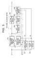
- Fig. 1 shows the optical information reproduction device of the first embodiment of the present invention.
- reference numeral 11 denotes an optical disk
- reference numeral 12 denotes a spindle motor
- reference numeral 13 denotes an optical head
- reference numeral 14 denotes a first I/V converting means
- reference numeral 15 denotes a second I/V converting means
- reference numeral 16 denotes an adding means
- reference numeral 18 denotes a subtracting means
- reference numeral 35 denotes a difference signal processing means
- reference numeral 36 denotes a signal switching means
- reference numeral 37 denotes a waveform shaping means
- reference numeral 22 denotes a reproduction clock generation means
- reference numeral 23 denotes a data demodulating means
- reference numeral 24 denotes an address information reproduction means
- reference numeral 25 denotes a control gate generation means that generates a control gate signal with reference to the timing of the address reproduction completion signal from the address information reproduction means 24.
- the difference signal processing means 35 comprises a buffer amplifier 351, reversing buffer amplifier 352, polarity switching signal generation means 353, and switching means 354.
- Fig. 1 The operation of the optical information reproduction device of the embodiment as described above for reproducing information from the optical disk shown in Fig. 11 will be described with reference to Fig. 1, Fig. 2A to Fig. 2K, and Fig. 3A to Fig. 3G.
- Fig. 2A to Fig. 2K and Fig. 3A to Fig. 3G show the waveforms at various points in Fig. 1.
- the output from the subtracting means 18 has a waveform as shown as (b) in Fig. 2B or (b') in Fig. 2C while the beam spot is scanning the center of a track.
- (b) and (b') indicate that the polarity of the output waveform from the subtracting means 18 depends on whether the track scanned by the beam spot is a land track or groove track. That is, the polarity of the output waveform depends on the direction of displacement of the identification information with respect to the position of the beam spot.
- a "track offset with respect to the identification information" is a maximum (this is because the identification information is shifted relative to the center of the track by half a track pitch).
- the difference between the outputs of the two-part split photodetector 135 is maximum, and the output (b) of the subtracting means 18, that is a push-pull signal, is maximum or minimum. Consequently, the signal reproduced from the first identification information shifted radially outward with respect to the track center and the signal reproduced from the second identification information shifted radially inward form a waveform with opposite polarities with respect to the zero level (or reference level).
- the beam spot scans the center of a track, and the outputs of the two-part split photodetector 135 are the same, and the output (b) from subtracting means 18 is zero (or reference level).
- an example of the polarity switching signal generation means 353 comprises a first gate generation means 281, a second gate generation means 291, and a polarity judging means 355.
- the polarity judging means 355 comprises an R-S flip-flop means 356 and an AND means 357.
- the polarity switching signal generation means 353 generates a discrimination gate signal (h) shown in Fig. 2H used to discriminate the first identification information from the output signal (b) of the subtracting means 18.
- the switching means 354 selects and outputs either the output (i) (shown in Fig. 2D) of the buffer amplifier 351 or the output (j) (shown in Fig. 2E) of the reversing buffer amplifier 352 to the signal switching means 36.
- the signal switching means 36 selects the output (a) of the adding means 16 and the output (k) of the difference signal processing means 35 according to the switching signal (1) (shown in Fig. 2J) from the control gate generation means 25, and supplies the selected outputs to the waveform shaping means 37.
- the switching signal can be generated by an internal timer, started by a timing of which position of appearance can be identified. An example of such a timing is the address detection completion timing signal from the address information reproduction means 24. If the reproduced identification information is detected from the output of the adding means 16 in the same way as the reproduced user information is detected, the control gate generation means 25 may be set to always select the output (a) of the adding means 16 for the signal switching means 36.
- the waveform shaping means 37 comprises a third gate generation means 371 which detects the user information area, a fourth gate generation means 372 which detects the position of a flaw on the medium, a boost gate generation means 373 which generates a first boost gate signal for changing the time constant of the direct-current component rejection, a direct-current component rejection means 374, and a signal slicing means 375.
- the signal slicing means 375 comprises a first binarization means 376, a slice level control means 377, a slice level adjustment means 378, and a second binarization means 379.
- the third gate generation means 371 detects the user information area from the signal (m) (shown in Fig. 2K, and in Fig. 3A) input by the signal switching means 36, and the fourth gate generation means detects the position of a flaw on the medium.
- the boost gate generation means 373 generates a first boost gate signal (q) (shown in Fig. 3E) having a predetermined period at the beginning of the first and second identification information in the identification information area and the beginning and end of the user information area, by means of a one-shot means.
- the direct-current component rejection means 374 decreases the time constant for the period of the first boost gate signal input from the boost gate generation means 373 and reduces the direct-current component from the output signal (m) of the signal switching means 36 at a high speed, thereby keeping substantially constant direct-current components in the output (a) from the adding means 16 and the output (k) from the difference signal processing means 35.
- processing is performed to keep the amplitude of the output signal of the direct-current component rejection means 374 to a constant value, degradation in waveform resulting from the frequency response of the optical system is separately improved (reduced) in the identification information area and in the user information area by an equalization means, which is not shown.
- the improvement for the identification information area and the improvement for the user information area are made separately.
- binarization is performed by the signal slicing means 375, and the waveform as shown as (n) shown in Fig. 3G is output.
- the signal slicing means 375 optimizes the slice level to minimize the reproduction error.
- the signal (r) shown in Fig. 3F) of which direct-current component has been removed by the direct-current component rejection means 374 is first converted into binary values by the first binarization means 376 at a specified slice level. Then, the slice level control means 377 adjusts the slice level to set the average duty ratio of the binary pulse to a specified value, and the slice level adjustment means 378 generates a second boost gate signal, so that the slice level is optimized at a high speed in the boost period.
- the slice level adjustment means 378 may apply an offset to the slice level mentioned above. This offset may be set to such a value that the reproduction jitter and the reproduction error rate are minimized. Further, the value may be separately set for the first identification information area, second identification information area, and user information area, or the value may be separately set, depending on whether the beam spot is scanning a land track or groove track. Moreover, the offset value may be adjusted according to the reproduction speed. Furthermore, the durations of the first and second boost gate signals may be set independently or may be varied according to the reproduction speed, error rate, or jitter.
- time constants of direct-current component rejection and slice level control may vary according to the reproduction speed.
- the operation for reproducing address information and user information from the output of the waveform shaping means 37 is the same as that in the prior art and will not be described here.
- Fig. 12 shows the details of the boost gate generation means 373. As illustrated, it includes first to fourth one-shot pulse generation means 401 to 404 respectively receiving the signals (d), (e), (o) and (p), and an OR gate 405 receiving the outputs of the one-shot pulse generation means 401 to 404. Each of the one-shot pulse generation means produces a pulse which rises at the rising edge of the input, and has a certain duration.
- Fig. 13 shows details of each of the one-shot pulse generation means 401 to 404.
- Fig. 14A to Fig. 14E shows the waveforms of the signals at various parts in the circuit of Fig. 13.
- the one-shot pulse generation means comprises a flip-flop 411 having its CK input connected to the input terminal IN and having its Q output connected to the output terminal OUT of the one-shot pulse generation means, a transistor 402 having its base connected to the /Q (inversion of Q) terminal of the flip-flop 411, a constant-current source 413 having its one end connected to the emitter of the transistor 412, a capacitor 414 connected across the collector and the emitter of the transistor 412, and a comparator 415 having a first input terminal connected to the emitter of the transistor 412, and a second input terminal connected to a reference voltage means 416.
- the output of the comparator 415 is connected to the reset terminal R of the flip-flop 411.
- the Q output of the flip-flop 411 goes “Low”
- the /Q output of the flip-flop 411 goes "High”.
- the transistor 412 is turned on, and the capacitor 414 is charged with a time constant dependent on the capacitance of the capacitor 414 and the driving capacity of the transistor.
- the potential on the first input of the comparator 415 rises, and when it exceeds the reference level Vref, the output of the comparator 415 goes from “Low” to "High".
- the upper limit of the input of the comparator 415 is the "High” level of the /Q output of the flip-flop 411 minus the base-to-emitter voltage V BE of the transistor 412.
- the output of the flip-flop 411 is a pulse which rises at the rising edge of the input signal to the input terminal IN and has a duration determined by the capacitance C of the capacitor 414 and the current I of the constant-current source 413, and the reference level Vref.
- the value of the current I of the constant-current source 413 is varied.
- the information for changing the duration of the pulse is provided in the form of an electric current, and the current I of the constant-current source 413 is set in an analog manner by the use of the current signal.
- a medium with a defect or flaw As shown in Fig. 6A to Fig. 6C, if the medium has a defect, the amplitude of the signal reproduced from the defective portion is reduced, varying the direct-current component of the signal and the slice level. Accordingly, the direct-current component and slice level need to be stabilized at a high speed immediately after the defective portion. Therefore, a fourth gate generation means 372 is provided so that the defective portion can be detected and the control time constant is reduced for a specified period immediately after the defect, thereby enabling high-speed stabilization.
- a defect increasing the signal amplitude can be processed in the same way. That is, if a defect or flaw causes such a large variation in the direct-current component that cannot be followed with the time constant in the steady state, the time constant is reduced after the end of such an area so that the direct-current component and slice level are stabilized at a high speed.
- the fourth gate generation means 372 detects the defective portion from the signal (m) (shown in Fig. 6A) input by the signal switching means 36 and outputs a flaw detection signal, which is not shown.
- the boost gate generation means 373 opens the boost gate for a specified period after the end of the defective portion according to the input flaw detection signal (p) (shown in Fig. 6C) and reduces the direct-current component at a high speed.
- the slice level adjustment means 378 opens the boost gate for a specified period after the end of the defective portion according to the input flaw detection signal, which is not shown, and adjusts the slice level at a high speed.
- the signal switching means 36 keeps selecting the output of the difference signal processing means 35 while the identification information area is being scanned.
- the signal switching means 36 selects the output of the difference signal processing mean 35 or the output of the adding means 16 according to the type of the disk, the probability of identification information detection, and the jitter in the reproduced identification information, so as to obtain a better result (lower error rate).
- "To select the output of the difference signal processing means 35" as recited in the appended claims should be construed to cover an arrangement where the selection of the output of the difference signal processing means 35 is continued throughout the period when the identification information area is being scanned, and an arrangement where the output of the difference signal processing means 35 and the output of the adding means 16 are selectively output according various conditions.
- the two-part split photodetector 135 is used.
- a photodetector such as four-part split photodetector, having more than two light-receiving parts may be used.
- the present invention produces the following effects.
- the switching means When the switching means is provided to switch between the difference signal and reverse difference signal according to the direction of the shift of the identification signal while the identification information is reproduced, the first identification information and second identification information can be made to have an identical polarity,
- the first identification information and second identification information can be made to have an identical polarity
- a direct-current component rejection means is provided to remove the direct-current component from the waveform of the difference signal and the waveform of the sum signal and the time constants for control are switched at the points where the variation in the level of the signal occurs, the waveform pattern of the difference signal and the waveform pattern of the sum signal can be made to be similar to each other at a high speed. Further, by switching the time constants for control immediately after a flaw in the medium, a return can also be made at a high speed.
- a slice level controlling means is provided to optimize the slice level of a signal with a predetermined time constant, and a slice level adjustment means is provided to add an offset to the slice level set by the slice level controlling means, an optimum slice level can be set and the probability of signal detection can be improved.
- slice level offset values are set separately for the first and second identification information and user information, an optimum slice level can be set and the probability of signal detection can be improved.
- the slice level can be optimized at a high speed. Moreover, the slice level can also be optimized at a high speed by decreasing the time constant of slice level control immediately after a flaw in the medium.
- the probability of signal detection can be improved at a variety of reproduction speeds.
- the probability of signal detection can be improved at a variety of reproduction speeds.
Landscapes
- Optical Recording Or Reproduction (AREA)
Claims (13)
- Schaltung zur Verwendung in einer Vorrichtung zum Wiedergeben von Informationen von einer optischen Scheibe mit Aufzeichnungsspuren, welche Scheibe einen Informationsbereich mit einem ersten Identifikationsinformationsbereich, der von der Mitte einer Aufzeichnungsspur radial nach außen verschoben ist, und einem zweiten Identifikationsinformationsbereich, der von der Mitte einer Aufzeichnungsspur radial nach innen verschoben ist, enthält, wobei die Vorrichtung einen Lichtdetektor (135) mit zumindest zwei Lichterfassungsbereichen aufweist, welche Schaltung Additionsmittel (16) zum Addieren der Ausgangssignale des Lichtdetektors und Subtraktionsmittel (18) zum Subtrahieren der Ausgangssignale des Lichtdetektors aufweist, und gekennzeichnet durch Mittel (352) zum Umkehren der Polarität mit Bezug auf einen Bezugspegel des Ausgangssignals der Subtraktionsmittel für die einen von den ersten und den zweiten Identifikationsinformationen zum Erzeugen eines Identifikationsinformationssignals mit derselben Polarität mit Bezug auf einen Bezugspegel für den ersten und den zweiten Identifikationsinformationsbereich.
- Schaltung nach Anspruch 1 für eine Vorrichtung weiterhin enthaltend einen optischen Kopf (13), der das optische Scheibenmedium mit einem Lichtstrahl beleuchtet, wobei der Lichtdetektor ein geteilter Fotodetektor (135) mit zumindest zwei Lichtempfangsteilen, die sich auf entgegengesetzten Seiten einer Spurentangentiallinie in dem Fernfeld des optischen Scheibenmediums befinden und von dem optischen Scheibenmedium reflektiertes Licht empfangen, ist, wobei auf der Scheibe die ersten Identifikationsinformationen radial auswärts mit Bezug auf die Mitte einer Aufzeichnungsspur um einen bestimmten Abstand verschoben sind und die zweiten Identifikationsinformationen mit Bezug auf die Mitte einer Aufzeichnungsspur um einen bestimmten Abstand radial nach innen verschoben sind, welche optische Scheibe weiterhin einen Benutzerinformationsbereich enthält, der entlang der Mitte einer Aufzeichnungsspur angeordnet ist, die eine konzentrische oder Spiralform aufweist,
wobei die Additionsmittel (16) die Ausgangssignale des geteilten Fotodetektors (135) addieren; die Subtraktionsmittel (18) eine Differenz zwischen den Ausgangssignalen des geteilten Fotodetektors (135) erhalten;
welche Schaltung weiterhin aufweist:Differenzsignal-Verarbeitungsmittel (35), die bewirken, dass das Ausgangssignal der Subtraktionsmittel (18) in Bezug auf die Polarität dem Ausgangssignal der Addiermittel (16) im Wellenformmuster aufweisend die Polaritätsumkehrmittel ähnlich gemacht wird;Signalauswahlmittel (36), die selektiv das Ausgangssignal der Additionsmittel (16) und das Ausgangssignal der Differenzsignal-Verarbeitungsmittel (35) ausgeben; undwellenform-Formungsmittel (37), die die auf dem Scheibenmedium aufgezeichneten Informationen in dem Ausgangssignal der Signalauswahlmittel (36) erfassen;welche Signalauswahlmittel (36) so eingestellt sind, dass sie das Ausgangssignal der Differenzsignal-Verarbeitungsmittel (35) oder das Ausgangssignal der Additionsmittel (36) auswählen, wenn der Identifikationsinformationsbereich abgetastet wird, und das Ausgangssignal der Additionsmittel (16) auswählen, wenn der Benutzerinformationsbereich abgetastet wird. - Schaltung nach Anspruch 2, bei der die Differenzsignal-Verarbeitungsmittel (35) weiterhin aufweisen:eine Auswahlvorrichtung (354) zum selektiven Ausgeben des Ausgangssignals der Subtraktionsmittel (18) und des Ausgangssignals der Polaritätsumkehrmittel (352); undPolaritätsumschaltsignal-Erzeugungsmittel (353) zum Erzeugen einer Umschaltzeit für die Auswahlmittel (354).
- Schaltung nach Anspruch 3, bei der die Polaritätsumechaltsignal-Erzeugungsmittel (353) aufweisen:erste Torerzeugungsmittel (281) zum Erzeugen eines ersten Torsignals, das die Position anzeigt, an der die ersten Identifikationsinformationen erscheinen;zweite Torerzeugungsmittel (282) zum Erzeugen eines zweiten Torsignals, das die Position anzeigt, an der die zweiten Identifikationsinformationen erscheinen; undPolaritätsbeurteilungsmittel (355) zum Beurteilen der Polarität der Wellenform des Ausgangssignals der Subtraktionsmittel (18).
- Schaltung nach Anspruch 2, bei der
die Wellenform-Formungsmittel (37) aufweisen; Gleichstromkomponenten-Zurückweisungsmittel (374) zum Entfernen der Gleichstromkomponente des Ausgangssignals der Signalauswahlmittel (36) mit einer vorbestimmten Zeitkonstante;
dritte Torerzeugungsmittel (371) zum Erzeugen eines Torsignals (o), das die Position anzeigt, an der die Benutzerinformationen erscheinen; vierte Torerzeugungsmittel (372) zum Erzeugen eines Torsignals (p), das die Position eines Defekts anzeigt;
Erhöhungstor-Erzeugungsmittel (373) zum Erzeugen eines ersten Erhöhungstorsignals (q) zum Ändern der Zeitkonstanten der Gleichstromkomponenten-Zurückweisungsmittel (374) gemäß den Ausgangssignalen der ersten Torerzeugungsmittel (281), der zweiten Torerzeugungsmittel (291), der dritten Torerzeugungsmittel (371) und der vierten Torerzeugungsmittel (373); und
Signalschneidmittel (375) zum Binärisieren des Ausgangssignals der Gleichstromkomponenten-Zurückweisungsmittel (374);
wobei die Gleichkomponenten-Zurückweisungsmittel (374) die Zeitkonstante während einer vorbestimmten Periode nach dem Beginn der ersten Identifikationsinformationen, dem Beginn der zweiten Identifikationsinformationen, dem Beginn der Benutzerinformationen und dem Ende des Defekts verringern. - Schaltung nach Anspruch 5, bei der die Signalschneidmittel (375) aufweisen:erste Binarisierungsmittel (376) zum Binärisieren des Ausgangssignals der Gleichstromkomponenten-Zurückweisungsmittel (374) bei einem Schneidpegel;Schneidpegel-Steuermittel (377) zum Steuern des Schneidpegels auf einen optimalen Wert mit einer vorbestimmten Zeitkonstanten auf der Grundlage des Ausgangssignals der ersten Binärisierungsmittel (376);Schneidpegel-Einstellmittel (378) zum Ausüben einer Versetzung auf den von den Schneidpegel-Steuermitteln (377) eingestellten Pegel; undzweite Binärisierungsmittel (379) zum Binärisieren des Ausgangssignals der Gleichstromkomponenten-Zurückweisungsmittel (374) an dem Ausgang der Schneidpegel-Einstellmittel (377).
- Schaltung nach Anspruch 6, bei der die Schneidpegel-Einstellmittel (378) ein zweites Erhöhungstorsignal mit vorbestimmter Dauer erzeugen, das gemäß den Ausgangssignalen der ersten bis vierten Torerzeugungsmittel erzeugt wurde, und die Zeitkonstante für die Steuerung des Schneidpegels während der Periode des zweiten Erhöhungstorsignals herabsetzen.
- Schaltung nach Anspruch 7, bei der die Erhöhungstor-Erzeugungsmittel (373) und die Schneidpegel-Einstellmittel (378) die Periode des Erhöhungstorsignals gemäß der Wiedergabegeschwindigkeit variieren können.
- Schaltung nach Anspruch 6, bei der die Gleichstromkomponenten-Zurückweisungsmittel und die Schneidpegel-Steuermittel die Zeitkonstante für die Steuerung variieren können.
- Schaltung nach Anspruch 6, bei der die Schneidpegel-Einstellmittel (378) die Versetzungswerte getrennt für die ersten Identifikationsinformationen, die zweiten Identifikationsinformationen und die Benutzerinformationen einstellen können.
- Vorrichtung zum Wiedergeben von Informationen von einer optischen Scheibe mit Aufzeichnungsspuren, welche Scheibe einen Informationsbereich mit einem ersten Identifikationsinformationsbereich, der von der Mitte einer Aufzeichnungsspur radial nach außen verschoben ist, und einen zweiten Identifikationsinformationsbereich, der von der Mitte einer Aufzeichnungsspur radial nach innen verschoben ist, enthält, wobei die Vorrichtung einen Lichtdetektor (135) mit zumindest zwei Lichterfassungsbereichen und eine Schaltung nach Anspruch 1 aufweist.
- Wiedergabevorrichtung für optische Informationen zum Wiedergeben von Informationen von einem optischen Scheibenmedium, auf dem ein Identifikationsinformationsbereich enthaltend erste Identifikationsinformationen, die mit Bezug auf die Mitte einer Aufzeichnungsspur um einen bestimmten Abstand radial nach außen verschoben sind, und zweite Identifikationsinformationen, die mit Bezug auf die Mitte einer Aufzeichnungsspur um einen vorbestimmten Abstand radial nach innen verschoben sind, und ein Benutzerinformationsbereich, der entlang der Mitte einer Aufzeichnungsspur verläuft, in konzentrischer oder Spitalform angeordnet sind, welche Wiedergabevorrichtung für optische Informationen die Schaltung nach Anspruch 2 und einen optischen Kopf (13) aufweist, bei der
der optische Kopf (13) das optische Scheibenmedium (11) mit einem Lichtstrahl beleuchtet und den geteilten Fotodetektor (135) mit zumindest zwei lichtempfangenden Teilen, die sich auf entgegengesetzten Seiten einer Spurtangentiallinie in dem Fernfeld des optischen Scheibenmediums befinden und von dem optischen Scheibemedium reflektiertes Licht empfangen, enthält. - Verfahren zum Wiedergeben von Informationen von einer optischen Scheibe mit Aufzeichnungsspuren und enthaltend einen Informationsbereich mit einem ersten Identifikationsinformationsbereich, der von der Mitte einer Aufzeichnungsspur radial nach außen verschoben ist, und einem zweiten Identifikationsinformationsbereich, der von der Mitte einer Aufzeichnungsspur radial nach innen verschoben ist, welches Verfahren aufweist: Erfassen von von dem Aufzeichnungsmedium reflektiertem Licht unter Verwendung eines Lichtdetektors mit zumindest zwei Lichterfassungsbereichen, Addieren der Ausgangssignale des Lichtdetektors, und Subtrahieren der Ausgangssignale des Lichtdetektors, dadurch gekennzeichnet, dass das Verfahren weiterhin aufweist:Umkehren der Polarität mit Bezug auf einen Bezugspegel des Ausgangssignals der Subtraktionsmittel für die einen der ersten und der zweiten Identifikationsinformationen, um ein Identifikationsinformationssignal mit derselben Polarität mit Bezug auf einen Bezugspegel für den ersten und den zweiten Identifikationsinformationsbereich zu erzeugen.
Applications Claiming Priority (2)
| Application Number | Priority Date | Filing Date | Title |
|---|---|---|---|
| JP2119998 | 1998-02-02 | ||
| JP02119998A JP3775914B2 (ja) | 1998-02-02 | 1998-02-02 | 光学的情報再生装置 |
Publications (3)
| Publication Number | Publication Date |
|---|---|
| EP0933758A2 EP0933758A2 (de) | 1999-08-04 |
| EP0933758A3 EP0933758A3 (de) | 2000-04-26 |
| EP0933758B1 true EP0933758B1 (de) | 2006-12-20 |
Family
ID=12048314
Family Applications (1)
| Application Number | Title | Priority Date | Filing Date |
|---|---|---|---|
| EP99300692A Expired - Lifetime EP0933758B1 (de) | 1998-02-02 | 1999-01-29 | Schaltung für optische Informationswiedergabevorrichtung, optisches Informationswiedergabevorrichtung und Verfahren zur Wiedergabe von Informationen |
Country Status (8)
| Country | Link |
|---|---|
| US (1) | US6320830B1 (de) |
| EP (1) | EP0933758B1 (de) |
| JP (1) | JP3775914B2 (de) |
| KR (1) | KR100308170B1 (de) |
| CN (1) | CN1184622C (de) |
| DE (1) | DE69934447T2 (de) |
| HK (1) | HK1022769A1 (de) |
| TW (1) | TW428168B (de) |
Families Citing this family (27)
| Publication number | Priority date | Publication date | Assignee | Title |
|---|---|---|---|---|
| JP3690177B2 (ja) * | 1999-02-22 | 2005-08-31 | 三菱電機株式会社 | ディスク装置 |
| US6891787B1 (en) * | 1999-08-24 | 2005-05-10 | Sanyo Electric Co., Ltd. | Apparatus for recording/reproducing signal on/from optical disk |
| US7088668B1 (en) * | 1999-10-19 | 2006-08-08 | Matsushita Electric Industrial Co., Ltd. | Optical recording medium with address information composed of pits |
| DE19961440A1 (de) * | 1999-12-20 | 2001-06-21 | Thomson Brandt Gmbh | Gerät zum Lesen und/oder Schreiben optischer Aufzeichnungsträger |
| JP3580292B2 (ja) * | 2002-03-20 | 2004-10-20 | 船井電機株式会社 | ディスク再生装置 |
| JP3519075B2 (ja) * | 2002-06-13 | 2004-04-12 | 沖電気工業株式会社 | 再生データ信号生成装置 |
| US20110181981A1 (en) * | 2005-05-09 | 2011-07-28 | Searete Llc, A Limited Liability Corporation Of The State Of Delaware | Method and system for rotational control of data storage devices |
| US8121016B2 (en) | 2005-05-09 | 2012-02-21 | The Invention Science Fund I, Llc | Rotation responsive disk activation and deactivation mechanisms |
| US7565596B2 (en) | 2005-09-09 | 2009-07-21 | Searete Llc | Data recovery systems |
| US7907486B2 (en) | 2006-06-20 | 2011-03-15 | The Invention Science Fund I, Llc | Rotation responsive disk activation and deactivation mechanisms |
| US7596073B2 (en) * | 2005-05-09 | 2009-09-29 | Searete Llc | Method and system for fluid mediated disk activation and deactivation |
| US8159925B2 (en) | 2005-08-05 | 2012-04-17 | The Invention Science Fund I, Llc | Limited use memory device with associated information |
| US8140745B2 (en) | 2005-09-09 | 2012-03-20 | The Invention Science Fund I, Llc | Data retrieval methods |
| US7770028B2 (en) | 2005-09-09 | 2010-08-03 | Invention Science Fund 1, Llc | Limited use data storing device |
| US7916592B2 (en) | 2005-05-09 | 2011-03-29 | The Invention Science Fund I, Llc | Fluid mediated disk activation and deactivation mechanisms |
| US9396752B2 (en) | 2005-08-05 | 2016-07-19 | Searete Llc | Memory device activation and deactivation |
| US7694316B2 (en) | 2005-05-09 | 2010-04-06 | The Invention Science Fund I, Llc | Fluid mediated disk activation and deactivation mechanisms |
| US7916615B2 (en) | 2005-06-09 | 2011-03-29 | The Invention Science Fund I, Llc | Method and system for rotational control of data storage devices |
| US8462605B2 (en) * | 2005-05-09 | 2013-06-11 | The Invention Science Fund I, Llc | Method of manufacturing a limited use data storing device |
| US8218262B2 (en) * | 2005-05-09 | 2012-07-10 | The Invention Science Fund I, Llc | Method of manufacturing a limited use data storing device including structured data and primary and secondary read-support information |
| US8220014B2 (en) | 2005-05-09 | 2012-07-10 | The Invention Science Fund I, Llc | Modifiable memory devices having limited expected lifetime |
| US8099608B2 (en) | 2005-05-09 | 2012-01-17 | The Invention Science Fund I, Llc | Limited use data storing device |
| US8264928B2 (en) | 2006-06-19 | 2012-09-11 | The Invention Science Fund I, Llc | Method and system for fluid mediated disk activation and deactivation |
| US8432777B2 (en) * | 2006-06-19 | 2013-04-30 | The Invention Science Fund I, Llc | Method and system for fluid mediated disk activation and deactivation |
| US20100124154A1 (en) * | 2008-11-19 | 2010-05-20 | Chih-Ching Yu | Signal processing devices and signal processing methods |
| JP2011065689A (ja) * | 2009-09-15 | 2011-03-31 | Jvc Kenwood Holdings Inc | 光ディスクドライブ装置 |
| JP5918146B2 (ja) * | 2010-01-25 | 2016-05-18 | アクセス ビジネス グループ インターナショナル リミテッド ライアビリティ カンパニー | 無線電力リンク上のデータ通信を検出するシステム及び方法 |
Family Cites Families (11)
| Publication number | Priority date | Publication date | Assignee | Title |
|---|---|---|---|---|
| JPS6357859A (ja) | 1986-08-27 | 1988-03-12 | Nippon Carbureter Co Ltd | 気化器の浮子弁装置 |
| JP2633417B2 (ja) | 1991-08-02 | 1997-07-23 | シャープ株式会社 | 光記録媒体駆動装置 |
| JPH0689473A (ja) * | 1992-09-10 | 1994-03-29 | Matsushita Electric Ind Co Ltd | 光磁気記録媒体 |
| US5452284A (en) * | 1992-09-14 | 1995-09-19 | Matsushita Electric Industrial Co., Ltd. | Optical recording/reproducing medium and apparatus using land and groove encoded information signals and identification signals including position information |
| JP2663817B2 (ja) * | 1992-12-02 | 1997-10-15 | 松下電器産業株式会社 | 光ディスク及びそれを用いた光ディスク装置 |
| US5444682A (en) * | 1993-09-07 | 1995-08-22 | Matsushita Electric Industrial Co., Ltd. | Tracking control apparatus |
| WO1996025736A1 (fr) | 1995-02-17 | 1996-08-22 | Matsushita Electric Industrial Co., Ltd. | Disque optique et dispositif d'enregistrement/de reproduction sur disque optique |
| US5872767A (en) * | 1995-02-17 | 1999-02-16 | Matsushita Electric Industrial Co., Ltd. | Optical disk and an optical disk recording/reproduction device having address blocks located on boundary lines between adjoining tracks |
| JP3063613B2 (ja) | 1996-03-25 | 2000-07-12 | 三菱電機株式会社 | 光ディスク媒体及び光ディスク装置 |
| JP3802189B2 (ja) | 1996-04-11 | 2006-07-26 | 松下電器産業株式会社 | 光学的情報記録再生装置及び記録再生方法 |
| US6044051A (en) * | 1996-04-11 | 2000-03-28 | Matsushita Electric Industrial Co., Ltd. | Optical information recording/reproducing device and method for recording, reproducing and erasing information on an optical information recording medium utilizing light beam radiation |
-
1998
- 1998-02-02 JP JP02119998A patent/JP3775914B2/ja not_active Expired - Fee Related
-
1999
- 1999-01-29 US US09/239,857 patent/US6320830B1/en not_active Expired - Fee Related
- 1999-01-29 DE DE69934447T patent/DE69934447T2/de not_active Expired - Lifetime
- 1999-01-29 EP EP99300692A patent/EP0933758B1/de not_active Expired - Lifetime
- 1999-01-30 KR KR1019990003022A patent/KR100308170B1/ko not_active IP Right Cessation
- 1999-02-01 TW TW088101462A patent/TW428168B/zh not_active IP Right Cessation
- 1999-02-02 CN CNB991017420A patent/CN1184622C/zh not_active Expired - Fee Related
-
2000
- 2000-03-09 HK HK00101475A patent/HK1022769A1/xx not_active IP Right Cessation
Also Published As
| Publication number | Publication date |
|---|---|
| JPH11219526A (ja) | 1999-08-10 |
| TW428168B (en) | 2001-04-01 |
| DE69934447D1 (de) | 2007-02-01 |
| CN1228580A (zh) | 1999-09-15 |
| US6320830B1 (en) | 2001-11-20 |
| HK1022769A1 (en) | 2000-08-18 |
| JP3775914B2 (ja) | 2006-05-17 |
| CN1184622C (zh) | 2005-01-12 |
| EP0933758A3 (de) | 2000-04-26 |
| KR19990072334A (ko) | 1999-09-27 |
| DE69934447T2 (de) | 2007-09-27 |
| KR100308170B1 (ko) | 2001-09-26 |
| EP0933758A2 (de) | 1999-08-04 |
Similar Documents
| Publication | Publication Date | Title |
|---|---|---|
| EP0933758B1 (de) | Schaltung für optische Informationswiedergabevorrichtung, optisches Informationswiedergabevorrichtung und Verfahren zur Wiedergabe von Informationen | |
| US6275466B1 (en) | Optical disk and optical disk drive device | |
| US5936932A (en) | Optical recording medium having ID part shifting from the center of groove tracks | |
| US5616390A (en) | Optical recording medium permitting detection of identification signals in land areas and groove areas, optical information recording/reproducing apparatus and apparatus for producing an original disk for forming a disk substrate | |
| US5745457A (en) | Optical disk player with coarse and fine speed control | |
| US6181655B1 (en) | Optical disc drive, timing signal generator, and information recording and reproduction method | |
| US5761171A (en) | Generating data detecting threshold levels from reference patterns recorded in an optical disk, such as a magneto-optical disk | |
| US5859820A (en) | Optical disk drive and optical disk having a continuous information track formed of alternating land and groove revolutions | |
| JP2807362B2 (ja) | 情報再生装置 | |
| US7706243B2 (en) | Method and apparatus for reproducing optical information | |
| KR100246968B1 (ko) | 광디스크에 기록된 정보재생장치 및 방법 | |
| KR100744846B1 (ko) | 기록/재생장치 및 기록/재생방법 | |
| JP2000123421A (ja) | 記録媒体、記録媒体製造装置及び情報記録再生装置 | |
| US6754145B1 (en) | Tilt compensation device for disk drive | |
| US5754505A (en) | Optical disc system with an optical disc having at least one channel of a multiple channel signal recorded on each side of a wobbling groove | |
| JP3846510B2 (ja) | 光学的情報再生装置 | |
| US7050372B2 (en) | Optical disk device configured to reliably reproduce address information | |
| JPH08297849A (ja) | スキュー制御装置 | |
| US6975569B2 (en) | Optical disk apparatus capable of generating clock accurately | |
| US20030227838A1 (en) | Optical disk and optical disk recording/reproducing apparatus | |
| KR20030053046A (ko) | 광디스크 장치 및 서보 제어 방법 | |
| KR20010036087A (ko) | 고밀도 디스크 기록매체와 그에 따른 데이터 재생장치 및 방법 | |
| GB2320362A (en) | Optical disk drive | |
| JPH0845110A (ja) | 光メモリ及び光メモリ再生装置 |
Legal Events
| Date | Code | Title | Description |
|---|---|---|---|
| PUAI | Public reference made under article 153(3) epc to a published international application that has entered the european phase |
Free format text: ORIGINAL CODE: 0009012 |
|
| AK | Designated contracting states |
Kind code of ref document: A2 Designated state(s): DE GB |
|
| AX | Request for extension of the european patent |
Free format text: AL;LT;LV;MK;RO;SI |
|
| PUAL | Search report despatched |
Free format text: ORIGINAL CODE: 0009013 |
|
| AK | Designated contracting states |
Kind code of ref document: A3 Designated state(s): AT BE CH CY DE DK ES FI FR GB GR IE IT LI LU MC NL PT SE |
|
| AX | Request for extension of the european patent |
Free format text: AL;LT;LV;MK;RO;SI |
|
| RIC1 | Information provided on ipc code assigned before grant |
Free format text: 7G 11B 7/00 A, 7G 11B 7/09 B |
|
| 17P | Request for examination filed |
Effective date: 20000425 |
|
| AKX | Designation fees paid |
Free format text: DE GB |
|
| 17Q | First examination report despatched |
Effective date: 20050221 |
|
| RAP1 | Party data changed (applicant data changed or rights of an application transferred) |
Owner name: MITSUBISHI DENKI KABUSHIKI KAISHA |
|
| GRAP | Despatch of communication of intention to grant a patent |
Free format text: ORIGINAL CODE: EPIDOSNIGR1 |
|
| RIC1 | Information provided on ipc code assigned before grant |
Ipc: G11B 7/09 20060101ALI20060602BHEP Ipc: G11B 7/005 20060101AFI20060602BHEP |
|
| RTI1 | Title (correction) |
Free format text: CIRCUIT FOR AN OPTICAL INFORMATION REPRODUCTION DEVICE, OPTICAL INFORMATION REPRODUCTION DEVICE AND METHOD OF REPRODUCING INFORMATION |
|
| GRAS | Grant fee paid |
Free format text: ORIGINAL CODE: EPIDOSNIGR3 |
|
| GRAA | (expected) grant |
Free format text: ORIGINAL CODE: 0009210 |
|
| AK | Designated contracting states |
Kind code of ref document: B1 Designated state(s): DE GB |
|
| REG | Reference to a national code |
Ref country code: GB Ref legal event code: FG4D |
|
| REF | Corresponds to: |
Ref document number: 69934447 Country of ref document: DE Date of ref document: 20070201 Kind code of ref document: P |
|
| PLBE | No opposition filed within time limit |
Free format text: ORIGINAL CODE: 0009261 |
|
| STAA | Information on the status of an ep patent application or granted ep patent |
Free format text: STATUS: NO OPPOSITION FILED WITHIN TIME LIMIT |
|
| 26N | No opposition filed |
Effective date: 20070921 |
|
| REG | Reference to a national code |
Ref country code: GB Ref legal event code: 746 Effective date: 20110513 |
|
| REG | Reference to a national code |
Ref country code: DE Ref legal event code: R084 Ref document number: 69934447 Country of ref document: DE Effective date: 20110506 Ref country code: DE Ref legal event code: R084 Ref document number: 69934447 Country of ref document: DE Effective date: 20110704 |
|
| PGFP | Annual fee paid to national office [announced via postgrant information from national office to epo] |
Ref country code: GB Payment date: 20130123 Year of fee payment: 15 Ref country code: DE Payment date: 20130123 Year of fee payment: 15 |
|
| REG | Reference to a national code |
Ref country code: DE Ref legal event code: R119 Ref document number: 69934447 Country of ref document: DE |
|
| GBPC | Gb: european patent ceased through non-payment of renewal fee |
Effective date: 20140129 |
|
| PG25 | Lapsed in a contracting state [announced via postgrant information from national office to epo] |
Ref country code: DE Free format text: LAPSE BECAUSE OF NON-PAYMENT OF DUE FEES Effective date: 20140801 |
|
| REG | Reference to a national code |
Ref country code: DE Ref legal event code: R119 Ref document number: 69934447 Country of ref document: DE Effective date: 20140801 |
|
| PG25 | Lapsed in a contracting state [announced via postgrant information from national office to epo] |
Ref country code: GB Free format text: LAPSE BECAUSE OF NON-PAYMENT OF DUE FEES Effective date: 20140129 |