EP0926818A2 - Amplificateur de classe A/F - Google Patents
Amplificateur de classe A/F Download PDFInfo
- Publication number
- EP0926818A2 EP0926818A2 EP98403000A EP98403000A EP0926818A2 EP 0926818 A2 EP0926818 A2 EP 0926818A2 EP 98403000 A EP98403000 A EP 98403000A EP 98403000 A EP98403000 A EP 98403000A EP 0926818 A2 EP0926818 A2 EP 0926818A2
- Authority
- EP
- European Patent Office
- Prior art keywords
- filtering
- amplifier
- circuit
- radio frequency
- input signal
- Prior art date
- Legal status (The legal status is an assumption and is not a legal conclusion. Google has not performed a legal analysis and makes no representation as to the accuracy of the status listed.)
- Granted
Links
Images

Classifications
-
- H—ELECTRICITY
- H03—ELECTRONIC CIRCUITRY
- H03F—AMPLIFIERS
- H03F3/00—Amplifiers with only discharge tubes or only semiconductor devices as amplifying elements
- H03F3/189—High-frequency amplifiers, e.g. radio frequency amplifiers
- H03F3/19—High-frequency amplifiers, e.g. radio frequency amplifiers with semiconductor devices only
- H03F3/193—High-frequency amplifiers, e.g. radio frequency amplifiers with semiconductor devices only with field-effect devices
-
- H—ELECTRICITY
- H03—ELECTRONIC CIRCUITRY
- H03F—AMPLIFIERS
- H03F1/00—Details of amplifiers with only discharge tubes, only semiconductor devices or only unspecified devices as amplifying elements
- H03F1/32—Modifications of amplifiers to reduce non-linear distortion
- H03F1/3205—Modifications of amplifiers to reduce non-linear distortion in field-effect transistor amplifiers
Definitions
- the present invention relates generally to amplifiers; and more particularly, to amplifiers for mobile communication systems using radio frequency multiple access signals.
- class A and F amplifiers for amplifying a radio frequency signal in a base station of a mobile radio communication system are known in the art.
- a class A nor a class F amplifier provides adequate harmonic filtering of the radio frequency signal.
- one disadvantage of the prior art class A and F amplifiers is that the harmonics in the radio frequency signal cause power interference between adjacent channels, resulting in degraded mobile communication service, including more dropped calls and a reduced calling range.
- the class A amplifier has appreciable power gain, produces a magnified replica of the input signal voltage or current wave, and is typically used in multimode or multi-signal transmitters where accurate reproduction of both the envelope and the phase of the signal is required.
- Tuned circuits or low-pass filters are not integral components of class A amplifiers, although they may be included to improve harmonic suppression.
- An example of the class A amplifier is shown and described on pages 352-355 (see Figure 12-3) of H.L. Krauss, Solid State Radio Engineering, John Wiley and Sons, New York, 1980.
- the nonlinearity in class A amplifiers produces two types of unwanted signals, called harmonics and intermodulation distortion (IMD) products.
- the IMD products (identified as third, fifth, seventh order products) are prominent near the carrier frequency. They cause distortion in the received signal and/or adjacent channel interference.
- the unwanted harmonics may be removed by filters, but the unwanted IMD products generally cannot be removed.
- Current code division multiple access (CDMA) amplifiers have a 15 dB peak to average ratio which greatly increases the IMD and harmonics.
- the class A amplifier also dissipates large amounts of power to amplify a signal due to the biasing operation in the center of a typical power amplifier load line. Thus the class A amplifier is not an efficient amplifier. Furthermore, the class A amplifier cannot suppress IMD products due to a lack of harmonic traps.
- class A amplifier under large signal conditions tends to self bias. This self bias moves toward shutting the device off, generating further harmonics and intermodulation products.
- a large signal condition is defined as an input signal that is strong enough to distort the output signal beyond the IS97 specification.
- the class F amplifier is characterized by a load network that has resonances at one or more harmonic frequencies as well as the carrier frequency.
- the class F amplifier has a transistor that usually operates as a current source or a saturating current source, similar in operation to a classical class C power amplifier.
- a third-harmonic peaking amplifier provides an example of the operation of the class F amplifier.
- the transistor acts as a current source, producing the same half-sine-wave similar in operation to a class B amplifier.
- the fundamental-frequency tune circuit bypasses the harmonics, producing a sinusoidal output voltage.
- the third-harmonic resonator makes possible a third-harmonic component in the collector voltage, which flattens the collector voltage.
- An example of a class F amplifier is shown and described on pages 454-458 (See Figure 14-9) of H.L. Krauss, Solid State Radio Engineering, John Wiley and Sons, New York, 1980.
- the class F amplifier does not amplify a signal linearly.
- the class F amplifier is essentially biased off, and strongly flattens the signal which introduces large amounts of IMD distortion. Thus the class F amplifier is not linear.
- the class F amplifier will not amplify low power signals. Thus if a signal is 10 dB below normal, then the class F amplifier will not amplify it. For example, CDMA signals with peak to average power ratios of 15 dB cannot be amplified linearly.
- the class F amplifier also has a radio frequency choke (RFC) which allows undesirable radio frequency harmonics to travel unfiltered through the amplifier.
- RRC radio frequency choke
- the invention provides a new kind of amplifier, known herein as a class A/F amplifier, that has an filtering and matching input circuit, a summing junction, an amplifying circuit, a filtering and feedback biasing circuit, and an output filtering and matching circuit.
- a class A/F amplifier that has an filtering and matching input circuit, a summing junction, an amplifying circuit, a filtering and feedback biasing circuit, and an output filtering and matching circuit.
- the filtering and matching input circuit responds to a radio frequency access input signal, for providing a filtered and matched radio frequency access input signal.
- the summing junction responds to the filtered and matched radio frequency access input signal, and further responds to a filtering and feedback biasing signal, for providing a summed, filtered, matched and feedback radio frequency access input signal.
- the amplifying circuit responds to the summed, filtered, matched and feedback radio frequency access input signal, for providing an amplified, summed, filtered, matched and feedback radio frequency access input signal.
- the feedback and filtering biasing circuit responds to the amplified, summed, filtered, matched and feedback radio frequency access input signal, for providing the feedback and filtering biasing signal.
- the output filtering and matching circuit responds to the amplified, summed, filtered, matched and feedback radio frequency access input signal, for providing an amplified, summed, filtered, matched and feedback radio frequency access output signal.
- the input and output filtering may include a combination of one or more circuits for distortion shunting, impedance matching or harmonic filtering.
- the unique filtering and feedback biasing circuit provides for a set range of bias conditions over a large range of input signals. Over this range of bias conditions the bias network maintains adequate bias and linearity. Additionally, the gate capacitor in and drain capacitor out are part of the feedback network, and adjust the amount and frequency of the feedback by their respective capacitance to minimize bias induced distortion.
- the class A/F amplifier is used in the mobile radio base station that receives the radio frequency access input signal from the mobile phone.
- the radio frequency access input signal may be either a frequency division multiple access (FDMA) signal, a time division multiple access (TDMA) signal, or a code division multiple access (CDMA) signal.
- FDMA frequency division multiple access
- TDMA time division multiple access
- CDMA code division multiple access
- One important advantage of the amplifier of the present invention is that there are substantially reduced harmonics in the amplified filter radio frequency access output signal to cause power interference between adjacent channels, resulting in greatly improved mobile communication service having much fewer dropped calls and a greatly improved calling range.
- the invention comprises the features of construction, combination of elements, and arrangement of parts which will be exemplified in the construction hereinafter set forth, and the scope of the invention will be indicated in the claims.
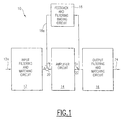
- Figure 1 shows a block diagram of a class A/F amplifier that is the subject matter of the present invention.
- Figure 2 shows a more detailed block diagram of the class A/F amplifier in Figure 1.
- Figure 3 is a schematic of the class A/F amplifier shown in Figures 1 and 2.
- Figure 4 is a graph of spectral regrowth of a 5.5 watt CDMA amplifier at 7 dB output power back-off.
- Figure 1 shows an embodiment of an amplifier, which will be referred to hereinafter as a class A/F amplifier, generally indicated as 10.
- the class A/F amplifier 10 has an input filtering and matching circuit generally indicated as 12, an amplifier circuit generally indicated as 14, an output filtering and matching circuit generally indicated as 16, a feedback and filtering biasing circuit generally indicated as 18, and a first summing junction 20.
- the input filtering and matching circuit 12 responds to a radio frequency access signal along line 12a, for providing a filtered and matched radio frequency access input signal.
- a summing junction 20 responds to the filtered and matched radio frequency access input signal, and further responds to a feedback and filtered biasing signal along line 18a, for providing a summed filtered, matched and feedback radio frequency access input signal.
- the amplifying circuit 14 responds to the summed filtered, matched and feedback radio frequency access input signal, for providing an amplified filtered, matched and feedback radio frequency access input signal to node 22.
- the feedback and filtering biasing circuit 17 responds to the amplified harmonically filtered radio frequency input signal at node 20, for providing the feedback and filtered biasing signal indicated as 18a.
- the output filtering and matching circuit 16 responds to the amplified filtered radio frequency access input signal indicated as 22, for providing an amplified filtered and matched radio frequency access output signal generally indicated as 24 to an output circuit (not shown).
- the input and output filtering may include a combination of one or more circuits for distortion shunting, impedance matching or harmonic filtering, all of which will be discussed in greater detail below.
- the class A/F amplifier 10 is used in a mobile radio base station (not shown) that receives the radio frequency access input signal 18 from a mobile phone (not shown).
- the radio frequency access input signal 18 may be either a frequency division multiple access (FDMA) signal, a time division multiple access (TDMA) signal, or a code division multiple access (CDMA) signal.
- FDMA frequency division multiple access
- TDMA time division multiple access
- CDMA code division multiple access
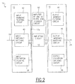
- Figure 2 shows a more detailed block diagram of the class A/F amplifier in Figure 1.
- the class A/F amplifier in Figure 2 includes the following: input distortion shunting circuits 38, an input impedance matching circuit 40 and an input harmonic filtering circuit 42.
- the class A/F amplifier 10 in Figure 2 includes the following: an output harmonic filtering circuit 44, an output impedance matching circuit 46 and an output distortion shunting circuit 48.
- the scope of the invention is not intended to be limited to any particular kind of distortion shunting, impedance matching or harmonic filtering circuits, all of which will be discussed in greater detail below.
- the radio frequency access input signal 18 is harmonically filtered on both the input and output sides of the amplifying circuit 14.
- the class A/F amplifier 10 in Figure 2 also has an amplifier RF and DC bias filtering and feedback circuit 50 connecting the input side to the output side of the amplifying circuit 14.
- the amplifier RF and DC bias filtering and feedback circuit 50 corresponds to the filtering and feedback biasing circuit 17 in Figure 1.
- the scope of the invention is not intended to be limited to any particular kind of amplifying, filtering or feedback circuit.
- the amplifying circuit 14 will be discussed in greater detail below with respect to Figure 3.
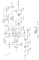
- Figure 3 is a schematic of the class A/F amplifier 10 in Figure 2.
- the summing junction 20 is shown as an amplifier input point a I in Figures 1 and 3 and the amplifier output point a O are also indicated in Figures 1 and 3.
- the input distortion shunting and output distortion shunting circuits 38, 48 provide a low pass harmonic short function to the input and output signals of the class A/F amplifier 10.
- the input distortion shunting circuit 38 and the output distortion shunting circuit 48 of Figure 2 are respectively indicated as STUBIN plus gate CAP IN and STUBOUT plus drain CAPOUT shown in Figure 3.
- the circuits STUBIN and STUBOUT in Figure 3 include an inductor and a capacitor connected in parallel to ground, not shown.
- the scope of the invention is not intended to be limited to any particular circuit design for the circuits STUBIN and STUBOUT in Figure 3.
- the inductor may be removed and the cap replaced with an open stub.
- the input and output impedance matching circuits 40, 46 in Figure 2 provide impedance matching for the class A/F amplifier 10 with an input or output circuit connected thereto (not shown).
- the input and output impedance matching circuit 40, 46 are generally indicated as INPTMCH and OUTPTMCH in Figure 3.
- the impedance matching circuits INPTMCH and OUTPTMCH include an inductor and a capacitor connected in parallel, not shown, and coupled to the amplifying circuit 14.
- the scope of the invention is not intended to be limited to any particular circuit design for the impedance matching circuits INPTMCH and OUTPTMCH in Figure 3.
- the amplifying circuit 14 in Figure 2 includes a field effect transistor (FET) generally indicated as TRANS in Figure 3, having a gate connection G, a drain connection D and a source connection S.
- FET field effect transistor
- the scope of the invention is not intended to be limited to any particular type of amplifying circuit, transistor or FET transistor.
- the input and output harmonic filtering circuits 42, 44 in Figure 2 provide input and output harmonic filtering of the radio frequency access input signal before and after amplification by the amplifier circuit 14.
- the input harmonic filtering circuit 42 in Figure 2 includes a second order input harmonic filtering circuit generally indicated as 2HARFLTIN in Figure 3, and also includes a third order input harmonic filtering circuit generally indicated as 3HARFLTIN also in Figure 3.
- the second order input harmonic filtering circuit 2HARFLTIN in Figure 3 filters even harmonics from the radio frequency access input signal.
- the third order input harmonic filtering circuit 3HARFLTIN filters odd harmonics from the radio frequency access input signal.
- the second order input harmonic filtering circuit 2HARFLTIN and the third order input harmonic filtering circuit 3HARFLTIN may include a bandstop filter that is tuned to eliminate the harmonics from the radio frequency access input signal.
- the bandstop filter also includes respective transmission lines, each having a length of about 1/8 of the operating frequency wavelength or an odd multiple thereof such as 3/8, 5/8 etc. and 1/12 of the operating frequency wave or a multiple thereof such as 3/6, 5/8 etc., not generally including any multiple of 1/4 of the operating frequency wavelength.
- Each field effect transistor (FET) will have distinct 2nd and 3rd harmonic load impedances required for best IMD supression. The load is tuned by slightly changing the lengths of these lines. The lines are also tuned to resonate out the even and odd has harmonies by grounding them.
- the bandstop filter may include an inductor and a capacitor connected in series (not shown) and coupled between the gate G of the transistor TRANS to ground.
- the output harmonic filtering circuit 44 in Figure 2 includes a second order input harmonic filtering circuit generally indicated as 2HARFLTOUT in Figure 3, and also includes a third order input harmonic filtering circuit generally indicated as 3HARFLTOUT also in Figure 3.
- the second order input harmonic filtering circuit 2HARFLTOUT in Figure 3 filters even harmonics from the amplified radio frequency access input signal.
- the third order input harmonic filtering circuit 3HARFLTOUT in Figure 3 filters odd harmonics from the amplified radio frequency access input signal.
- the second order input harmonic filtering circuit 2HARFLTOUT and the third order input harmonic filtering circuit 3HARFLTOUT may include a bandstop filter that is tuned to eliminate the harmonics from the radio frequency access input signal.
- the bandstop filter also has transmission lines respectively having a length of about 1/8 of the operating frequency wavelength or an odd multiple thereof such as 3/8, 5/8 etc. and 1/12 of the operating frequency wave or a multiple thereof such as 3/6, 5/8 etc., not generally including any multiple of 1/4 of the operating frequency wavelength.
- each FET will have distinct 2nd and 3rd harmonic load impedances required for best IMD supression.
- the is load is tuned by slightly changing the lengths of these lines.
- the lines are tuned to resonate out the even and odd has harmonies by grounding them.
- the bandstop filter may include an inductor and a capacitor (not shown) coupled between the drain D of the transistor TRANS to ground.
- the input and output harmonic filtering circuits 42, 44 in Figure 2 may include a bias or harmonic filter cap circuit.
- the filter cap circuit includes one or more capacitors generally indicated as C1-C4 and C8-C11, one or more inductors generally indicated as L1-L4 or one or more resistors R1 coupled to ground, all shown in Figure 3.
- These components in the prior art functioned as bias caps. In the present invention, these components perform optional filtering to reduce IMD distortion in the input harmonic filtering network.
- a capacitor C3 provides a filtering cap for the second order input harmonic filtering circuit 2HARFLTIN
- a capacitor C4 provides a filtering cap for the third order input harmonic filtering circuit 3HARFLTIN
- a capacitor C9 provides a filtering cap for the second order input harmonic filtering circuit 2HARFLTOUT
- a shuntstub generally indicated as SHNTSTB
- capacitors C8, C8A provide a filtering cap for the third order input harmonic filtering circuit 3HARFLTOUT.
- the shuntstub circuit SHNTSTB and the capacitors C8, C8A when used together have produced enhanced performance for the amplifier as a whole.
- the shuntstub circuit SHNTSTB includes an inductor and a capacitor connected in parallel to the output impedance matching circuit 46.
- capacitors generally indicated as CIN, COUT provide a DC bypassing function on the input and output sides of the class A/F amplifier 10.
- the field effect transistor TRANS has the feedback circuit or connection 50 between the drain D and the gate 6 for suppressing oscillations in the class A/F amplifier, that also includes a DO feedback resistor R2 to minimize the effect of DC changes during ageing, a RF feedback resistor R3 to minimize the effect of RF changes during ageing, and a feedback bypass capacitor C6.
- the feedback is adjusted to minimize self bias generated distortion, which works in depletion mode devices.
- the scope of the invention is not intended to be limited to embodiments having such a feedback circuit or connection 50.
- the class A/F amplifier of the present invention encompasses the advantages of both the class A and class F amplifiers combined and eliminates the disadvantages thereof. Specifically, the class A/F amplifier of the present invention uses a bias point halfway between the class A and F amplifiers. Thus the class A/F amplifier is more efficient than class A, and more linear than class F.
- the class A/F amplifier has the high power gain of the class A amplifier and also amplifies reduced power signals, while having the harmonic filters of the class F amplifier, thus suppressing IMD signals.
- the most significant advantage of the present invention is that the class A/F amplifier filters, when operated at a class A bias, significantly reduce the intermodulation distortion (IMD), which the class A amplifier normally cannot suppress.
- IMD intermodulation distortion
- the class A/F amplifier suppresses the IMD while maximizing linear efficiency.
- the class A/F amplifier having the aforementioned novel matching network has been shown to increase the CDMA power and linear efficiency when compared to a class A amplifier.
- the simple, inexpensive class F amplifier structure suppresses the 3rd and 5th order products more than 10 dB over the class A amplifier.
- a 6.5 watt CDMA PCS class A/F amplifier demonstrated 20% linear efficiency: a threefold improvement in linear efficiency over typical PCS base station having the class A amplifier.
- the 6.5 watt amplifier demonstrated a 2.7 times improvement in linear power over a similar class A amplifier (power matched but without the class F traps).
- the class A/F amplifier improves linear power when compared to the class A amplifier, by using a series of harmonic traps and filters, while maintaining intersymbol interference levels through an intrinsic cosine filter. Linearity is not degraded by unequal power tones as in the class A/B amplifiers.
- the class A/F amplifier of the present invention uses four similar filters on the input and the output as well, as shown in Figure 3.
- the filter next to the transistor TRANS is a single pole shunt capacitor, which is labeled gate capacitor CAPIN on the input and drain capacitor CAPOUT on the output.
- the capacitors gate CAPIN and drain CAPOUT plus the intrinsic inductance of the transistor TRANS act as low pass filters, and slightly round the output from pulse to pulse which suppresses the spectral regrowth. These capacitors also are used with the feedback to adjust the amount of self biasing.
- the next filter is a pair of series tanks to ground, which consist of a short piece of transmission line ended with a cap shorted to ground.
- One series filter resonates (minimizes) the even harmonics which is labeled 2HARFLTIN (input), and 2HARFLTOUT (output) and the other filter resonates (minimizes) the odd harmonics which are labeled 3HARFLTIN (input), and 3HARFLTOUT (output).
- the last and final filter/matching network is a series quarter-wave-line at the third harmonic followed by open stubs, which are labeled STUBIN and STUBOUT.
- the final filter/matching network acts as a third harmonic short.
- One selection criteria for the transistor is to pick one that has the highest linear efficiency. This can be accomplished by load pulling transistors under two-tone drive conditions to determine which has the greatest linear efficiency.
- LDMOS Lateral Drain Metal Oxide Semiconductor
- BJT Bipolar Junction Transistors
- IM3 ratios i.e. 3rd Order Intermodulation Products
- a single stage LDMOS class A/F amplifier was tested. While operating with the class F components removed and with power matching, the single stage LDMOS class A/F amplifier operated at IS-97 linearity levels of 2.4 watts. When operating with the class F network attached, the single stage LDMOS class A/F amplifier produced 5.5 watts of linear IS-97 power levels as shown in Figure 8. Noise levels (CDMA spec levels) of the amplifiers were compared. The class A/F amplifier did not increase the noise floor. Both amplifiers were operated at the same bias power of 37 watts. Therefore, the class A efficiency was 6.4%, while the class A/F efficiency was 17.3%.
- class A/F amplification provides improved linear efficiency when compared to class A and class AB amplifiers.
- a three fold improvement in linear efficiency was found, which was accomplished by reducing the second and third harmonics through use of class F traps.
- the class A/F amplifier of the present invention is also an important contribution to the state of the art for other reasons: It has been shown that CDMA (a common spread spectrum signal) is a noise-like signal immune at a minimum of 30 dB to spurious non spread-spectrum signals. The CDMA is also susceptible to its own spectral regrowth interference, which limits the system capacity. Thus, for PCS CDMA systems to operate most cost effectively, inexpensive linear power amplifiers are required. Power amplifier linearity is determined by transistor performance and signal parameters. First, transistor performance parameters such as gate rectification or nonlinear variation of transistor charge are significant causes of nonlinearity.
- CDMA signals have reduced linearity for multiple reasons:
- Commercial PCS systems operate under wideband-width BPSK-DS-SS modulation at a high modulation rate with a two sigma statistical peak of 6 dB peak to average ratio.
- the harmonics and their associated intermodulation components can be quite strong which results in intersymbol interference and the associated BER degradation limiting the capacity of the PCS CDMA wireless system.
- the powers (summed Taylor coefficients) of each carrier are determined to be (A 2 )/50 and each of the third order products are determined to be (((A 3 )/4) 2 )/50. These coefficients (and further measurements) show that at saturated output power the third order distortion products will be 12 dB down below the carrier. Shorting out the harmonic mathematically removes the 2f2-f1 term and the 2f1-f2 term. Measurements show that the terms are reduced more than 20 dB. When implemented these networks allow the transistor to be operated much closer to saturation than a non-class F transistor.
- the CDMA amplifiers have a 15 dB peak to average ratio.
- the amplifiers output power was backed-off 7 dB, when compared to the typically required 11 dB back-off from a bipolar junction transistor.
- the class A/F amplifier is backed off only 7 dB while operated at the bias of a class A amplifier backed off 11 dB. Therefore, the class A/F amplifier has 4 dB more output power than the class A amplifier at the same linearity, with an associated improvement in efficiency.
- a class F amplifier is a class B amplifier which has additional harmonic-suppression-networks for development of a squarer wave form which improves efficiency, as shown in Figure 4.
- the class A/F amplifier when operated at its most efficient point is not very linear. But when backed off the class A/F amplifier is more linear and efficient than the class A amplifier.
- the industry custom is to use a class A/B amplifier to amplify the signal. When one biases the class A/B amplifier, it is more linear and efficient with a pair of equal tones than the class A amplifier. But, when the tones are not of equal strength, the class A/B amplifier is self biased by the higher of the two tones which suppresses and distorts the lower of the two tones.
- the class A/B amplifier acts like a limited filter which distorts lower power signals and in the process generates higher noise power.
- the class A/B amplifier increased the amplifier efficiency at the cost of link efficiency.
- the scope of the invention is not intended to be limited to an amplifier for amplifying only a radio frequency access input signal, like the frequency division multiple access (FDMA) signal, the time division multiple access (TDMA) signal, or the code division multiple access (CDMA) signal.
- the thrust of the invention relates to harmonic filtering of any signal before and after amplification.
- the amplifier is a class A/F amplifier having a harmonic filtering circuit that responds to any input signal, for providing a harmonically filtered input signal, and further responds to an amplified harmonically filtered input signal, for providing any amplified harmonically filtered output signal.
- the class A/F amplifier has an amplifying circuit that responds to the harmonically filtered input signal, for providing the amplified harmonically filtered input signal.
- the harmonic filtering circuit also has an input harmonic filtering circuit for filtering harmonics from the input signal, and output harmonic filtering circuit for filtering harmonics from the amplified harmonically filtered input signal. (The input filtering removes transistor generated distortion.)
- the input harmonic filtering circuit has a second order input harmonic filtering circuit for filtering even harmonics from the input signal, and a third order input harmonic filtering circuit for filtering odd harmonics from the input signal.
- the output harmonic filtering circuit has a second order output harmonic filtering circuit for filtering even harmonics from the amplified harmonically filtered input signal, and a third order output harmonic filtering circuit for filtering odd harmonics from the amplified harmonically filtered input signal.
Landscapes
- Engineering & Computer Science (AREA)
- Power Engineering (AREA)
- Physics & Mathematics (AREA)
- Nonlinear Science (AREA)
- Amplifiers (AREA)
- Transceivers (AREA)
- Transmitters (AREA)
- Mobile Radio Communication Systems (AREA)
Applications Claiming Priority (2)
| Application Number | Priority Date | Filing Date | Title |
|---|---|---|---|
| US988565 | 1997-12-11 | ||
| US08/988,565 US5969575A (en) | 1997-12-11 | 1997-12-11 | Class A/F amplifier having second and third order harmonic input and output filtering and self bias distortion correction |
Publications (3)
| Publication Number | Publication Date |
|---|---|
| EP0926818A2 true EP0926818A2 (fr) | 1999-06-30 |
| EP0926818A3 EP0926818A3 (fr) | 2004-06-16 |
| EP0926818B1 EP0926818B1 (fr) | 2007-04-04 |
Family
ID=25534267
Family Applications (1)
| Application Number | Title | Priority Date | Filing Date |
|---|---|---|---|
| EP98403000A Expired - Lifetime EP0926818B1 (fr) | 1997-12-11 | 1998-11-30 | Amplificateur de classe A/F |
Country Status (6)
| Country | Link |
|---|---|
| US (1) | US5969575A (fr) |
| EP (1) | EP0926818B1 (fr) |
| JP (1) | JP3228909B2 (fr) |
| KR (1) | KR100339674B1 (fr) |
| CA (1) | CA2248888C (fr) |
| DE (1) | DE69837467T2 (fr) |
Cited By (4)
| Publication number | Priority date | Publication date | Assignee | Title |
|---|---|---|---|---|
| EP1119102A3 (fr) * | 2000-01-18 | 2004-06-16 | Sanyo Electric Co., Ltd. | Circuit de contre-réaction et amplificateur et mélangeur comprenant ledit circuit |
| GB2407931A (en) * | 2003-11-04 | 2005-05-11 | Agilent Technologies Inc | Power amplifier with improved linearity |
| EP2020752A1 (fr) | 2007-08-02 | 2009-02-04 | SiRiFIC Wireless Corporation | Système sans fil disposant d'une pureté spectrale élevée |
| GB2507169A (en) * | 2012-08-31 | 2014-04-23 | Shun Fu Technology Corp | Designing filters for a radio frequency circuit to suppress frequency-multiplied harmonics and intermodulation distortions |
Families Citing this family (28)
| Publication number | Priority date | Publication date | Assignee | Title |
|---|---|---|---|---|
| EP0827649A1 (fr) * | 1996-03-20 | 1998-03-11 | Koninklijke Philips Electronics N.V. | Circuit de preaccentuation pour signal analogique dans un reseau de videocommunication |
| US6246283B1 (en) | 1999-03-09 | 2001-06-12 | Tripath Technology, Inc. | Power efficient line driver |
| WO2001026217A1 (fr) * | 1999-09-30 | 2001-04-12 | Fujitsu Limited | Amplificateur de puissance haute frequence |
| US6501332B1 (en) * | 2000-07-13 | 2002-12-31 | Texas Instruments Incorporated | Apparatus and method for electrical signal amplification |
| EP1344315B1 (fr) * | 2000-10-10 | 2008-03-26 | California Institute Of Technology | Amplificateurs de puissance de commutation de classe e/f |
| KR20030096861A (ko) * | 2002-06-18 | 2003-12-31 | 엘지전자 주식회사 | 전압제어를 통한 주파수 변경 가능한 고주파 증폭기 |
| US6859118B2 (en) * | 2003-01-02 | 2005-02-22 | Harris Corporation | System and method for an ultra low noise micro-wave coaxial resonator oscillator using ⅝ths wavelength resonator |
| US6961553B2 (en) * | 2003-04-11 | 2005-11-01 | Motorola, Inc. | Bidirectional distributed amplifier |
| JP4688410B2 (ja) * | 2003-07-15 | 2011-05-25 | スタンレー電気株式会社 | 広帯域増幅器 |
| KR100749932B1 (ko) * | 2004-03-05 | 2007-08-16 | 아바고테크놀로지스코리아 주식회사 | 바이패스 스위치를 사용하지 않는 다중 전력 모드 전력증폭 장치 |
| US7215221B1 (en) * | 2004-08-30 | 2007-05-08 | Hrl Laboratories, Llc | Harmonic termination circuit for medium bandwidth microwave power amplifiers |
| US7176769B1 (en) * | 2004-11-29 | 2007-02-13 | Hrl Laboratories, Llc | Harmonic termination circuit for medium bandwidth microwave power amplifiers |
| KR100623062B1 (ko) * | 2005-01-13 | 2006-09-14 | 인하대학교 산학협력단 | 고조파 제거 회로 |
| US7391211B2 (en) * | 2005-11-08 | 2008-06-24 | Continental Automotive Systems Us, Inc. | Digital fluxgate magnetometer |
| US7974402B2 (en) * | 2007-03-28 | 2011-07-05 | Harris Corporation | TDMA mobile ad-hoc network (MANET) with second order timing and tracking |
| US8885630B2 (en) * | 2007-06-14 | 2014-11-11 | Harris Corporation | TDMA communications system with configuration beacon and associated method |
| JP5242480B2 (ja) * | 2009-03-27 | 2013-07-24 | 古河電気工業株式会社 | 広帯域バイアス回路 |
| US8344801B2 (en) * | 2010-04-02 | 2013-01-01 | Mks Instruments, Inc. | Variable class characteristic amplifier |
| JP5720545B2 (ja) * | 2011-11-24 | 2015-05-20 | 富士通株式会社 | 電力増幅器 |
| US8456238B1 (en) * | 2012-03-30 | 2013-06-04 | Centellax, Inc. | Tapered attenuator network for mitigating effects of direct current (DC) bias inductor self-resonance in traveling wave amplifiers |
| WO2014110435A1 (fr) * | 2013-01-11 | 2014-07-17 | Rfaxis, Inc. | Filtrage d'harmonique sur puce pour des amplificateurs de puissance de radiofréquence |
| US10418951B2 (en) | 2015-03-24 | 2019-09-17 | Skyworks Solutions, Inc. | Combined output matching network and filter for power amplifier with concurrent functionality |
| JP6815564B2 (ja) * | 2018-06-27 | 2021-01-20 | 三菱電機株式会社 | 電力増幅器及びフィルタ |
| TWI676349B (zh) * | 2018-08-17 | 2019-11-01 | 立積電子股份有限公司 | 放大電路 |
| CN110784185B (zh) * | 2019-11-11 | 2023-08-01 | 北京普能微电子科技有限公司 | 功率放大器、输出匹配电路和射频模块 |
| CN112928999A (zh) * | 2019-12-05 | 2021-06-08 | 恩智浦美国有限公司 | 一种放大器及其制造方法 |
| US11817832B2 (en) | 2020-01-03 | 2023-11-14 | Skyworks Solutions, Inc. | Power amplifier output matching |
| JP2023000811A (ja) * | 2021-06-18 | 2023-01-04 | 住友電気工業株式会社 | 高調波処理回路および増幅装置 |
Family Cites Families (8)
| Publication number | Priority date | Publication date | Assignee | Title |
|---|---|---|---|---|
| JPS5341963A (en) * | 1976-09-28 | 1978-04-15 | Mitsubishi Electric Corp | Negative feedback amplifier circuit |
| DE3020313C2 (de) * | 1980-05-29 | 1982-05-19 | Rohde & Schwarz GmbH & Co KG, 8000 München | Verstärkerstufe zum Verstärken amplitudenmodulierter Frequenzsignale |
| US4774477A (en) | 1987-03-18 | 1988-09-27 | Rockwell International Corporation | Power amplifier having low intermodulation distortion |
| FR2651622B1 (fr) | 1989-08-18 | 1991-10-31 | Thomson Composants Microondes | Amplificateur a haut rendement. |
| US5166639A (en) * | 1991-10-29 | 1992-11-24 | Sgs-Thomson Microelectronics, Inc. | High gain mololithic microwave integrated circuit amplifier |
| GB9126616D0 (en) * | 1991-12-16 | 1992-02-12 | Texas Instruments Ltd | Improvements in or relating to amplifiers |
| US5420536A (en) * | 1993-03-16 | 1995-05-30 | Victoria University Of Technology | Linearized power amplifier |
| FR2704112B1 (fr) * | 1993-04-13 | 1995-05-24 | Thomson Lgt | Dispositif d'amplification de signaux de télévision à classe de fonctionnement variable, prédéterminée pour l'élimination des erreurs de transmission. |
-
1997
- 1997-12-11 US US08/988,565 patent/US5969575A/en not_active Expired - Lifetime
-
1998
- 1998-10-15 CA CA002248888A patent/CA2248888C/fr not_active Expired - Fee Related
- 1998-11-05 JP JP31419998A patent/JP3228909B2/ja not_active Expired - Fee Related
- 1998-11-30 DE DE69837467T patent/DE69837467T2/de not_active Expired - Lifetime
- 1998-11-30 EP EP98403000A patent/EP0926818B1/fr not_active Expired - Lifetime
- 1998-12-10 KR KR1019980054270A patent/KR100339674B1/ko not_active Expired - Fee Related
Cited By (6)
| Publication number | Priority date | Publication date | Assignee | Title |
|---|---|---|---|---|
| EP1119102A3 (fr) * | 2000-01-18 | 2004-06-16 | Sanyo Electric Co., Ltd. | Circuit de contre-réaction et amplificateur et mélangeur comprenant ledit circuit |
| GB2407931A (en) * | 2003-11-04 | 2005-05-11 | Agilent Technologies Inc | Power amplifier with improved linearity |
| EP2020752A1 (fr) | 2007-08-02 | 2009-02-04 | SiRiFIC Wireless Corporation | Système sans fil disposant d'une pureté spectrale élevée |
| EP2323268A1 (fr) * | 2007-08-02 | 2011-05-18 | Icera Canada ULC | Système sans fil disposant d'une pureté spectrale élevée |
| GB2507169A (en) * | 2012-08-31 | 2014-04-23 | Shun Fu Technology Corp | Designing filters for a radio frequency circuit to suppress frequency-multiplied harmonics and intermodulation distortions |
| GB2507169B (en) * | 2012-08-31 | 2017-02-15 | Shun-Fu Tech Corp | Frequency-multiplied harmonic supression method for RF circuit |
Also Published As
| Publication number | Publication date |
|---|---|
| EP0926818B1 (fr) | 2007-04-04 |
| CA2248888C (fr) | 2001-12-04 |
| DE69837467D1 (de) | 2007-05-16 |
| JPH11234052A (ja) | 1999-08-27 |
| JP3228909B2 (ja) | 2001-11-12 |
| EP0926818A3 (fr) | 2004-06-16 |
| CA2248888A1 (fr) | 1999-06-11 |
| KR100339674B1 (ko) | 2002-07-18 |
| US5969575A (en) | 1999-10-19 |
| KR19990062976A (ko) | 1999-07-26 |
| DE69837467T2 (de) | 2008-05-15 |
Similar Documents
| Publication | Publication Date | Title |
|---|---|---|
| US5969575A (en) | Class A/F amplifier having second and third order harmonic input and output filtering and self bias distortion correction | |
| US11824501B2 (en) | Power amplifier circuit | |
| US7202736B1 (en) | CDMA power amplifier design for low and high power modes | |
| KR101089891B1 (ko) | 무선 통신 장치용 집적 전력 증폭기 시스템 | |
| EP1576724B1 (fr) | Amplificateur de puissance radioelectrique utilisant des topologies de circuit de polarisation pour reduire au minimum les effets de memoire | |
| US6392492B1 (en) | High linearity cascode low noise amplifier | |
| CA2351327C (fr) | Reseaux d'adaptation d'impedance pour circuits non lineaires | |
| EP1364457B1 (fr) | Circuit permettant de lineariser des dispositifs electroniques | |
| US20200195202A1 (en) | RF Power Amplifiers with Diode Linearizer | |
| Kang et al. | Design of Doherty power amplifiers for handset applications | |
| US20020050856A1 (en) | Scheme for reducing transmit-band noise floor and adjacent channel power with power backoff | |
| Cho et al. | Compact design of linear Doherty power amplifier with harmonic control for handset applications | |
| Bailey | Intermodulation distortion in pseudomorphic HEMTs and an extension of the classical theory | |
| JP2002305414A (ja) | 周波数変換回路 | |
| CN216625700U (zh) | 一种l波段功放模块 | |
| JP3698647B2 (ja) | 前置歪補償回路および電力増幅装置 | |
| CN115882795B (zh) | 一种具备线性化补偿结构的功率放大器 | |
| CN118199527A (zh) | 一种低互调宽带射频放大器 | |
| Liu et al. | A Broadband InP Darlington Amplifier with Two-Way Distributed Power Combining | |
| Saraswat et al. | Transformer Based Waveform Engineered Power Amplifier in a 65 nm Bulk-CMOS Process | |
| Fedorenko | Phase distortion in envelope elimination and restoration radio frequency power amplifiers | |
| Mydin et al. | A 960 MHz Area Efficient CMOS Power Amplifier with Integrated Active Load APD for RFID Application | |
| CN119788006A (zh) | 一种具有功率检测的高线性度高功率的GaAs HBT功率放大器 | |
| WO2003012982A2 (fr) | Circuit d'amortissement accorde pour sortie d'amplificateur de puissance | |
| Matsubara et al. | Simultaneous 3rd-and-5th-order intermodulation compensation with cuber predistortion and 2nd harmonics injection for microwave power amplifiers |
Legal Events
| Date | Code | Title | Description |
|---|---|---|---|
| PUAI | Public reference made under article 153(3) epc to a published international application that has entered the european phase |
Free format text: ORIGINAL CODE: 0009012 |
|
| AK | Designated contracting states |
Kind code of ref document: A2 Designated state(s): AT BE CH CY DE DK ES FI FR GB GR IE IT LI LU MC NL PT SE |
|
| AX | Request for extension of the european patent |
Free format text: AL;LT;LV;MK;RO;SI |
|
| PUAL | Search report despatched |
Free format text: ORIGINAL CODE: 0009013 |
|
| AK | Designated contracting states |
Kind code of ref document: A3 Designated state(s): AT BE CH CY DE DK ES FI FR GB GR IE IT LI LU MC NL PT SE |
|
| AX | Request for extension of the european patent |
Extension state: AL LT LV MK RO SI |
|
| 17P | Request for examination filed |
Effective date: 20041029 |
|
| AKX | Designation fees paid |
Designated state(s): DE FR GB IT SE |
|
| GRAP | Despatch of communication of intention to grant a patent |
Free format text: ORIGINAL CODE: EPIDOSNIGR1 |
|
| GRAS | Grant fee paid |
Free format text: ORIGINAL CODE: EPIDOSNIGR3 |
|
| GRAA | (expected) grant |
Free format text: ORIGINAL CODE: 0009210 |
|
| AK | Designated contracting states |
Kind code of ref document: B1 Designated state(s): DE FR GB IT SE |
|
| REG | Reference to a national code |
Ref country code: GB Ref legal event code: FG4D |
|
| REF | Corresponds to: |
Ref document number: 69837467 Country of ref document: DE Date of ref document: 20070516 Kind code of ref document: P |
|
| PG25 | Lapsed in a contracting state [announced via postgrant information from national office to epo] |
Ref country code: SE Free format text: LAPSE BECAUSE OF FAILURE TO SUBMIT A TRANSLATION OF THE DESCRIPTION OR TO PAY THE FEE WITHIN THE PRESCRIBED TIME-LIMIT Effective date: 20070704 |
|
| ET | Fr: translation filed | ||
| PLBE | No opposition filed within time limit |
Free format text: ORIGINAL CODE: 0009261 |
|
| STAA | Information on the status of an ep patent application or granted ep patent |
Free format text: STATUS: NO OPPOSITION FILED WITHIN TIME LIMIT |
|
| 26N | No opposition filed |
Effective date: 20080107 |
|
| REG | Reference to a national code |
Ref country code: FR Ref legal event code: TP Owner name: ALCATEL LUCENT, FR Effective date: 20130628 |
|
| REG | Reference to a national code |
Ref country code: GB Ref legal event code: 732E Free format text: REGISTERED BETWEEN 20130822 AND 20130828 |
|
| REG | Reference to a national code |
Ref country code: FR Ref legal event code: GC Effective date: 20130920 |
|
| REG | Reference to a national code |
Ref country code: FR Ref legal event code: RG Effective date: 20141016 |
|
| REG | Reference to a national code |
Ref country code: FR Ref legal event code: PLFP Year of fee payment: 18 |
|
| PGFP | Annual fee paid to national office [announced via postgrant information from national office to epo] |
Ref country code: GB Payment date: 20151118 Year of fee payment: 18 Ref country code: IT Payment date: 20151125 Year of fee payment: 18 Ref country code: DE Payment date: 20151119 Year of fee payment: 18 |
|
| PGFP | Annual fee paid to national office [announced via postgrant information from national office to epo] |
Ref country code: FR Payment date: 20151119 Year of fee payment: 18 |
|
| REG | Reference to a national code |
Ref country code: DE Ref legal event code: R119 Ref document number: 69837467 Country of ref document: DE |
|
| GBPC | Gb: european patent ceased through non-payment of renewal fee |
Effective date: 20161130 |
|
| REG | Reference to a national code |
Ref country code: FR Ref legal event code: ST Effective date: 20170731 |
|
| PG25 | Lapsed in a contracting state [announced via postgrant information from national office to epo] |
Ref country code: FR Free format text: LAPSE BECAUSE OF NON-PAYMENT OF DUE FEES Effective date: 20161130 Ref country code: IT Free format text: LAPSE BECAUSE OF NON-PAYMENT OF DUE FEES Effective date: 20161130 |
|
| PG25 | Lapsed in a contracting state [announced via postgrant information from national office to epo] |
Ref country code: GB Free format text: LAPSE BECAUSE OF NON-PAYMENT OF DUE FEES Effective date: 20161130 Ref country code: DE Free format text: LAPSE BECAUSE OF NON-PAYMENT OF DUE FEES Effective date: 20170601 |