EP0918409A2 - Robuste digitale Modulations- und Demodulationsart für Funkübertragung unter Fading-Bedingungen - Google Patents
Robuste digitale Modulations- und Demodulationsart für Funkübertragung unter Fading-Bedingungen Download PDFInfo
- Publication number
- EP0918409A2 EP0918409A2 EP98121593A EP98121593A EP0918409A2 EP 0918409 A2 EP0918409 A2 EP 0918409A2 EP 98121593 A EP98121593 A EP 98121593A EP 98121593 A EP98121593 A EP 98121593A EP 0918409 A2 EP0918409 A2 EP 0918409A2
- Authority
- EP
- European Patent Office
- Prior art keywords
- bits
- unit
- orthogonal code
- transmitting side
- value
- Prior art date
- Legal status (The legal status is an assumption and is not a legal conclusion. Google has not performed a legal analysis and makes no representation as to the accuracy of the status listed.)
- Withdrawn
Links
Images


Classifications
-
- H—ELECTRICITY
- H04—ELECTRIC COMMUNICATION TECHNIQUE
- H04L—TRANSMISSION OF DIGITAL INFORMATION, e.g. TELEGRAPHIC COMMUNICATION
- H04L25/00—Baseband systems
- H04L25/38—Synchronous or start-stop systems, e.g. for Baudot code
- H04L25/40—Transmitting circuits; Receiving circuits
- H04L25/49—Transmitting circuits; Receiving circuits using code conversion at the transmitter; using predistortion; using insertion of idle bits for obtaining a desired frequency spectrum; using three or more amplitude levels ; Baseband coding techniques specific to data transmission systems
- H04L25/4906—Transmitting circuits; Receiving circuits using code conversion at the transmitter; using predistortion; using insertion of idle bits for obtaining a desired frequency spectrum; using three or more amplitude levels ; Baseband coding techniques specific to data transmission systems using binary codes
- H04L25/4908—Transmitting circuits; Receiving circuits using code conversion at the transmitter; using predistortion; using insertion of idle bits for obtaining a desired frequency spectrum; using three or more amplitude levels ; Baseband coding techniques specific to data transmission systems using binary codes using mBnB codes
-
- H—ELECTRICITY
- H04—ELECTRIC COMMUNICATION TECHNIQUE
- H04J—MULTIPLEX COMMUNICATION
- H04J13/00—Code division multiplex systems
- H04J13/0007—Code type
- H04J13/004—Orthogonal
-
- H—ELECTRICITY
- H04—ELECTRIC COMMUNICATION TECHNIQUE
- H04J—MULTIPLEX COMMUNICATION
- H04J13/00—Code division multiplex systems
- H04J13/10—Code generation
- H04J13/12—Generation of orthogonal codes
-
- H—ELECTRICITY
- H04—ELECTRIC COMMUNICATION TECHNIQUE
- H04L—TRANSMISSION OF DIGITAL INFORMATION, e.g. TELEGRAPHIC COMMUNICATION
- H04L23/00—Apparatus or local circuits for systems other than those covered by groups H04L15/00 - H04L21/00
- H04L23/02—Apparatus or local circuits for systems other than those covered by groups H04L15/00 - H04L21/00 adapted for orthogonal signalling
Definitions
- the present invention relates to a digital modulation and demodulation scheme for radio communications between a terminal and a base station such as those of the mobile communication, and more particularly, to a digital modulation and demodulation scheme for radio communications which is robust against variation of receiving signal strength due to fading and capable of reducing occurrences of errors.
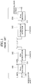
- Fig. 1 shows a configuration of a conventional M-ary modulation and demodulation system, which comprises an M-ary encoder 101, a PSK (Phase Shift Keying) modulator 102, a synchronous detector 103, and an M-ary decoder 104.
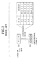
- M 4 so that 2 bits (a1, a2) of the entered data are converted into one of the 4 bits length orthogonal codes C 1 to C 4 according to a conversion rule shown in Fig. 2, and then outputted.
- the PSK modulator 102 applies the bi-phase shift keying (BPSK) to a carrier by using this orthogonal code.
- BPSK bi-phase shift keying
- a signal is detected by the synchronous detector 103, and the M-ary decoder 104 calculates cross-correlation value by multiplying the detected signal with each one of the four possible orthogonal codes C 1 to C 4, and determines the orthogonal code with the highest cross-correlation value as a received signal.
- the M-ary decoder 104 outputs 2 bits of the original data corresponding to the determined orthogonal code according to the conversion rule shown in Fig. 2.
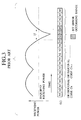
- the orthogonal code that encountered this receiving power dropping due to fading (which appear shaded in Fig. 3) is difficult to detect using the correlation because of thermal noise, and therefore it has a higher probability of being decoded erroneously as another orthogonal code, and when such an erroneous decoding occurs, the bursty error of about L bits length will be caused.
- Fig. 4 shows a configuration of a transmitting side of the conventional modulation and demodulation system.
- orthogonal code generators 203-1 to 203-4 employ 4-ary orthogonal codes obtained from 4 ⁇ 4 Hadamard matrix, and therefore a shift register 202 stores data in 2 bits length.
- the input data entered from an input terminal 201 is stored in the shift register 202.
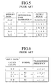
- a processor 204 reads out these bits from the shift register 202, selects a corresponding one of the orthogonal code generators 203-1 to 203-4 according to a conversion rule shown in Fig. 5, and outputs a bit sequence outputted from the selected orthogonal code generator to the frequency modulator 205.
- the relationship between the input bits, the 4-valued symbols and the transmission frequencies in this case is shown in Fig. 6.
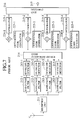
- Fig. 7 shows a configuration of a receiving side of the conventional modulation and demodulation system.
- the desired radio signals received at a reception unit 211 are entered into four band-pass filters 212-1 to 212-4 having the central frequencies ranging from ⁇ c+ ⁇ 2 to ⁇ c- ⁇ 2.
- Each band-pass filter outputs only a signal having a frequency component in a prescribed bandwidth.
- the output signals of the band-pass filters are entered into corresponding envelope detectors 213-1 to 213-4, where voltage values or power values of the signals are obtained.
- the voltage values are to be obtained, and the voltage values obtained in correspondence to the symbols (S1, S2, S3, S4) will be denoted as (e1, e2, e3, e4).
- These voltage values are entered into a code judgement device 214, where the symbol with the largest voltage value among four voltage values entered therein is selected, and bits corresponding to the selected symbol are obtained according to a correspondence table shown in Fig. 6.
- the obtained bits are then multiplied with output bits of orthogonal code generators 223-1 to 223-4 at multiplexers 224-1 to 224-4 and entered into integrators 215-1 to 215-4.
- integrators integrate the entered values over a transmission time required for 2 bits that are stored into the shift register at the transmitting side, and enters the obtained values into a decoding unit 216.
- This decoding unit 216 selects one input with the largest value among the four inputs, obtains 2 bits corresponding to one of the orthogonal code generators 223-1 to 223-4 that is used in multiplication of that input, and outputs these bits at an output terminal 217.
- a digital modulation and demodulation system for radio communications comprising: a transmitting side device having: a division unit for dividing transmission data in advance, into blocks of LN bits length each, where L and N are natural number greater than one, and dividing each block into N sets of L bits data sequences; an encoding unit for generating orthogonal codes of M bits length each, where M is a natural number, which are uniquely defined with respect to L bits codes given by the L bits data sequences obtained by the division unit; a multiplexing unit for multiplexing N sets of orthogonal codes generated by the encoding unit for each block into a multiplexed signal, such that M bits constituting each orthogonal code are dispersed in time in the multiplexed signal; and a modulation unit for applying a digital modulation to a carrier using the multiplexed signal obtained by the multiplexing unit; and a receiving side device having: a detection unit for obtaining a detection output of signals received from the transmitting side;
- a method of digital modulation and demodulation for radio communications comprising the steps of: (a) dividing transmission data in advance, into blocks of LN bits length each, where L and N are natural number greater than one, and dividing each block into N sets of L bits data sequences, at a transmitting side; (b) generating orthogonal codes of M bits length each, where M is a natural number, which are uniquely defined with respect to L bits codes given by the L bits data sequences obtained by the step (a), at the transmitting side; (c) multiplexing N sets of orthogonal codes generated by the step (b) for each block into a multiplexed signal, such that M bits constituting each orthogonal code are dispersed in time in the multiplexed signal, at the transmitting side; (d) applying a digital modulation to a carrier using the multiplexed signal obtained by the step (c), at the transmitting side; (e) obtaining a detection output of signals received from the transmitting side, at a
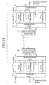
- Fig. 8 shows a configuration of a digital modulation and demodulation system in this first embodiment, in which a transmitting side comprises a division unit 5 for dividing LN bits data to be transmitted into N sets of L bits data sequences, N sets of M-ary encoders 1-1 to 1-N, a multiplexing unit 6 for multiplexing N sets of orthogonal codes, and a PSK modulator 2, while a receiving side comprises a synchronous detector 3, a separation unit 7 for separating detected signals into N sets of M bits sequences, N sets of M-ary decoders 4-1 to 4-N, and a composition unit 8 for recovering the original LN bits data by applying an inverse operation of what was applied at the transmitting side with respect to N sets of L bits data sequences.
- a transmitting side comprises a division unit 5 for dividing LN bits data to be transmitted into N sets of L bits data sequences, N sets of M-ary encoders 1-1 to 1-N, a multiplexing unit 6 for multiplexing N sets of orthogonal codes,
- digital signals entered at a modulation input terminal are divided into blocks of LN bits size each (where L and N are natural numbers greater than 1) at the division unit 5, and each block is further divided into N sets of L bits data sequence and entered into respective ones of the M-ary encoders 1-1 to 1-N.
- M-ary orthogonal codes corresponding to the respective inputs are generated similarly as in the conventional case.
- the 2 bits data (a1, a2) entered into the M-ary encoder 1-k (1 ⁇ k ⁇ N) is converted into one of the 4 bits length orthogonal codes C 1 to C 4 according to a conversion rule shown in Fig. 2 described above, and then outputted.
- N sets of orthogonal codes so obtained are then multiplexed at the multiplexing unit 6, and the output of the multiplexing unit 6 is entered into the PSK modulator 2 and used in phase modulating a carrier therein.
- Fig. 9 shows an exemplary signal processing up to the input of the PSK modulator 2 in Fig. 8.
- the input signal (a) (at a point (a) indicated in Fig. 8) is divided into blocks of 8 bits size each, and each set of 8 bits is further divided into 4 sequences of 2 bits each and entered into the M-ary encoders 1-1 to 1-4.
- the method for dividing each set of 8 bits into 4 sequences is arbitrary, and Fig. 9 depicts an exemplary case of forming a sequence from each 2 bits in the input order.
- the multiplexing unit 6 multiplexes signals outputted from the four M-ary encoders in bit units.
- 4 bits of the orthogonal code outputted from the M-ary encoder 1-1 are arranged at four hatched locations (b11, b12, b13, b14) in a demodulator input (d) (at a point (d) indicated in Fig. 8), while 4 bits of the orthogonal code outputted from the M-ary encoder 1-2 are arranged at four locations (b21, b22, b23, b24) which are displaced from (b11, b12, b13, b14) by one bit each, and so on.
- the signals are detected at the synchronous detector 3, and the detected signals are entered into the separation unit 7 where the detected signals are set into reception data-units of NM bits length each in synchronization with the multiplexing at the transmitting side.
- the separation unit 2 further separates each reception data-unit into N sets of M bits sequences and outputs them respectively to the M-ary decoders 4-1 to 4-N.
- the cross-correlation values are calculated by multiplying the entered detected signal with each one of the possible orthogonal codes, and the orthogonal code with the highest correlation value is judged as a received signal.
- the original L bits data corresponding to the orthogonal code that is judged as a received signal is obtained according to the same conversion rule as used at the transmitting side and outputted.
- the composition unit 8 then recovers the original LN bits data by applying the inverse operation of what was applied at the transmitting side with respect to N sets of L bits data sequence outputted from all the M-ary decoders.
- Fig. 10 shows an exemplary signal processing subsequent to the output of the synchronous detector 3 in Fig. 8, which is in correspondence to Fig. 9.
- the four times multiplexed detector output (e) (at a point (e) indicated in Fig. 8) is separated into four data sequences by the separation unit 7 using the inverse operation of what was applied by the multiplexing unit 6 at the transmitting side.
- the separated four data sequences are then respectively entered into the M-ary decoders 4-1 to 4-4.
- the orthogonal code with the highest correlation value with respect to the input is judged as a received signal, and the original 2 bits data corresponding to this orthogonal code that is judged as a received signal are obtained according to the same conversion rule of Fig. 2 as used at the transmitting side and then outputted.
- the four sequences of 2 bits data outputted from the M-ary decoders 4-1 to 4-4 are then recomposed into the original 8 bits data (f) (at a point (f) indicated in Fig. 8) by the composition unit 8 using the inverse operation of what was applied at the transmitting side.
- the reason why it is hard to cause errors by the receiving power dropping due to fading in this embodiment will be described.
- the 4 bits orthogonal code corresponding to the input data bit a1 (or a2) at a shaded location in the input signal (a) is arranged at locations b11 to b14 which are dispersed in time in the modulator input (d). Consequently, only one bit at b14 falls within the receiving power dropping time Tf due to fading shown in Fig. 10 (which is assumed to be identical to Tf shown in Fig. 3). As a result, the probability for being erroneously judged as another orthogonal code at a time of the correlation detection is low.
- 4 bits of one orthogonal code are arranged consecutively so that plural bits (4 bits in the case shown in Fig. 3) fall within the receiving power dropping time due to fading and therefore the probability for being erroneously judged as another orthogonal code is high.
- Fig. 8 shows an exemplary case of using the PSK synchronous detection as the modulation and demodulation method.
- the PSK synchronous detection cannot follow the abrupt carrier phase rotation.
- FSK Frequency Shift Keying
- Fig. 11 to Fig. 14 the second embodiment of a digital modulation and demodulation scheme for radio communications according to the present invention will be described in detail. This second embodiment is directed to the case of using multi-valued modulation method.
- Fig. 11 shows a configuration of a digital modulation and demodulation system in this second embodiment, where the division unit 5 and the M-ary modulators 1-1 to 1-N on the transmitting side and the M-ary decoders 4-1 to 4-N and the composition unit 8 on the receiving side are substantially similar to those of the first embodiment, while a multiplexing unit 9 and a separation unit 12 are adapted to handle multi-valued modulation, and a multi-valued modulator 10 and a multi-valued detector 11 are provided in places of the PSK modulator 2 and the synchronous detector 3 of Fig. 8.
- the operation in the second embodiment will be described mainly for a section from the multiplexing unit 9 to the separation unit 12 which differs from the first embodiment.
- the operation and the signal state at each component in a section from the modulation input terminal to the input of the multiplexing unit 9 are the same as in the case of Fig. 8.
- the multiplexing unit 9 multiplexes N sets of orthogonal codes and outputs signal sequences in number corresponding to the multi-valued number.
- the output of the multiplexing unit 9 is entered into the multi-valued modulator 10 and used in multi-valued modulating a carrier therein.
- Fig. 12 shows an exemplary signal processing up to the input of the multi-valued modulator 10 in Fig. 11.
- the input signal (a) (at a point (a) indicated in Fig. 11) is divided into blocks of 8 bits size each, and each set of 8 bits is further divided into 4 sequences of 2 bits each and entered into the M-ary encoders 1-1 to 1-4.
- the multiplexing unit 9 multiplexes signals outputted from the four M-ary encoders in bit units.
- signals from the M-ary encoders 1-1 and 1-3 are multiplexed into a sequence (g1) while signals from the M-ary encoders 1-2 and 1-4 are multiplexed into a sequence (g2) (at a point (g) indicated in Fig. 11).
- 4 bits of the orthogonal code outputted from the M-ary encoder 1-1 are arranged at four hatched locations (b11, b12, b13, b14) in the sequence (g1)
- 4 bits of the orthogonal code outputted from the M-ary encoder 1-2 are arranged at four locations (b21, b22, b23, b24) in the sequence (g2), and so on.
- the 4-valued modulation can be carried out by regarding 2 bits at the same timing in the sequences (g1) and (g2) as one symbol.
- Fig. 13 shows a configuration of a 4-valued FSK modulator 13 and a 4-valued FSK energy detector 14 in the case of using 4-valued FSK energy detection.
- the 4-valued FSK modulator 13 two modulator inputs g1 and g2 are entered, and frequencies corresponding to the values of g1 and g2 as indicated in a table shown below the 4-valued FSK modulator 13 are outputted.
- Fig. 14 shows an exemplary signal processing subsequent to the output of the multi-valued detector 11 in Fig. 11, which is in correspondence to Fig. 10.
- the four times multiplexed detector output (h1) and (h2) (at a point (h) indicated in Fig. 11) is separated into four data sequences by the separation unit 12 using the inverse operation of what was applied by the multiplexing unit 9 at the transmitting side.
- the separated four data sequences are then respectively entered into the M-ary decoders 4-1 to 4-4.
- the orthogonal code with the highest correlation value with respect to the input is judged as a received signal, and the original 2 bits data corresponding to this orthogonal code that is judged as a received signal are obtained according to the same conversion rule of Fig. 2 as used at the transmitting side and then outputted.
- the four sequences of 2 bits data outputted from the M-ary decoders 4-1 to 4-4 are then recomposed into the original 8 bits data (i) (at a point (i) indicated in Fig. 11) by the composition unit 8 using the inverse operation of what was applied at the transmitting side.
- the reason why it is hard to cause errors by the receiving power dropping due to fading in this embodiment will be described.
- the 4 bits orthogonal code corresponding to the input data bit a1 (or a2) at a shaded location in the input signal (a) is arranged at locations b11 to b14 which are dispersed in time in the modulator input (g1). Consequently, only one bit at b14 falls within the receiving power dropping time Tf due to fading shown in Fig. 14 (which is assumed to be identical to Tf shown in Fig. 3 and Fig. 10), similarly as in the first embodiment.
- the probability for being erroneously judged as another orthogonal code at a time of the correlation detection is low, so that it is possible to reduce the occurrences of bursty errors due to fading compared with the conventional case, just like the first embodiment.
- the number N of divisions greater than or equal to the above described number G of sequences. For the larger number N of divisions, the effect of the dispersion in time becomes greater and it becomes possible to further reduce the occurrences of bursty errors due to fading.
- the multi-valued modulation and demodulation method it is possible to use various known methods besides the multi-valued FSK energy detection, such as the multi-valued PSK synchronous detection and the 16 QAM (Quadrature Amplitude Modulation) pilot synchronous detection.
- the multi-valued FSK energy detection such as the multi-valued PSK synchronous detection and the 16 QAM (Quadrature Amplitude Modulation) pilot synchronous detection.
- the effect of the dispersion in time becomes greater and it becomes possible to further reduce the occurrences of bursty errors due to fading.
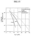
- the orthogonal code to be transmitted is dispersed over N times greater length on the time axis before transmission, and the orthogonal code in the state of being dispersed in time (which contains noise) is detected by correlation at the receiving side, so as to avoid the influence of the receiving power dropping due to fading and recover the original signal on the time axis, so that it is possible to reduce the occurrences of bursty errors due to fading and therefore it is possible to reduce the required reception S/N ratio.
- CDMA scheme it becomes possible to increase the capacity.
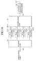
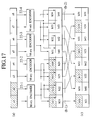
- Fig. 16 to Fig. 21 the third embodiment of a digital modulation and demodulation scheme for radio communications according to the present invention will be described in detail.
- This third embodiment is directed to a specific decoder configuration suitable for the digital modulation and demodulation scheme of the present invention described above.
- Fig. 16 shows a configuration of a transmitting side of the modulation and demodulation system in this third embodiment
- Fig. 17 shows a signal processing in this transmitting side of Fig. 16.
- bit sequence (a) at a modulation input is entered into a division unit 21.
- the division unit 17 enters 2 bits sequences constituting this bit sequence (a) into respective M-ary encoders 22-1 to 22-4, and each M-ary encoder outputs 4 bits length orthogonal code corresponding to the input.
- the orthogonal codes are then entered into a multiplexing unit 23 so as to multiplex outputs of the M-ary encoders into a series of symbol sequence (c).
- the multiplexing unit 23 carries out the multiplexing such that outputs from two M-ary encoders are taken together as one symbol and outputs (b-1) and (b-2) are arranged alternately in the symbol sequence (c), because the 4-valued frequency modulation is to be carried out.
- the output symbol sequence (c) of the multiplexing unit 23 is then entered into a 4-valued frequency modulator 24 and the 4-valued frequency modulation is carried out therein.
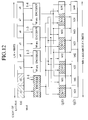
- Fig. 19 shows a configuration of a receiving side of the modulation and demodulation system in this third embodiment.
- signals received at a reception unit 31 are entered into four band-pass filters (BPF) 32-1, 32-2, 32-3 and 32-4 having the central frequencies ⁇ 1, ⁇ 2, ⁇ 3 and ⁇ 4, respectively.
- the output signals of the band-pass filters are entered into corresponding envelope detectors 33-1 to 33-4 to obtain detector output signals (d-1) to (d-4) which are then entered into a separation unit 35. Then, as shown in Fig.
- the separation unit 35 applies the inverse operation of what was applied by the multiplexing unit 23, i.e., takes detector output signals (d-1) to (d-4) that are outputted at the same timing as one set, and separates it into two output sequences (e-1) and (e-2), which are then entered into corresponding decoders 36-1 and 36-2 respectively.
- the detector output signal that appears hatched in Fig. 20 is obtained by energy detecting a signal in which bits that appear hatched in Fig. 17 are modulated.
- the outputs of the decoders 36-1 and 36-2 are then entered into a composition unit 37 where they are composed together to form an output bit sequence (h) which is outputted at a demodulation output.
- Fig. 21 shows an internal configuration of the decoder 36-1 in the configuration of Fig. 19.
- the decoder 36-2 also has the similar internal configuration.
- the detector output signal (e-1) after the separation is multiplied with each one of energy detection output patterns generated in advance by 2 L ⁇ G sets of processors 41-1 to 41-16.
- the processors 41 are provided with as many as the total number of patterns that can be generated by pairing each orthogonal code generator used at the transmitting side with every orthogonal code generator used at the transmitting side.
- every element of the orthogonal code generated by each orthogonal code generator is applied with a conversion which converts a bit with a value 0 into a value -1 and leaves a bit with a value 1 unchanged.
- This conversion is applied here for the sake of later convenience because a value 0 will be inconvenient in calculating a product at the subsequent calculation.
- G sets of converted M bits length orthogonal code C'n [C' n1, C' n2, ⁇ , C' nM ] (which can be regarded as a row vector) are arranged vertically to form a G ⁇ M matrix which defines codes W r given by the following equation (1), because as many as G sequences entered into the frequency modulator will be multi-valued.
- t w i [C' 1i, C' 2i, ⁇ , C' Gi ] (row vector)
- t denotes transpose
- r 1 to 2 L ⁇ G .
- W 1 1, 1, 1, 1 1, 1, 1, 1
- W 3 to W 16 are also generated by the processors 42-3 to 42-16.
- This decoding unit 44 selects the processor 41 that is used in obtaining the integrated signal which has the largest value among all the entered integrated signals, and outputs a bit sequence before the M-ary encoding which corresponds to the two orthogonal codes that are entered into that selected processor 41.
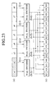
- Fig. 22 to Fig. 25 the fourth embodiment of a digital modulation and demodulation scheme for radio communications according to the present invention will be described in detail.
- This fourth embodiment is directed to another specific decoder configuration suitable for the digital modulation and demodulation scheme of the present invention described above.
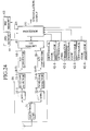
- Fig. 22 shows a configuration of a transmitting side of the modulation and demodulation system in this third embodiment
- Fig. 23 shows a signal processing in this transmitting side of Fig. 22.
- bit sequence (a) at a modulation input is entered into a division unit 21.
- the division unit 17 enters 2 bits sequences constituting this bit sequence (a) into respective M-ary encoders 22-1 to 22-4, and these M-ary encoders output 4 bits length orthogonal codes (b-3) to (b-6) corresponding to their respective inputs, similarly as in the third embodiment.
- the orthogonal codes are then entered into a multiplexing unit 23 so as to multiplex outputs of the M-ary encoders into a series of symbol sequence (c).
- the 2-valued frequency modulation is to be carried out so that one symbol comprises one bit, and therefore, as shown in Fig.
- the multiplexing unit 23 carries out the multiplexing such that outputs (b-3), (b-4), (b-5) and (b-6) are arranged alternately in the symbol sequence (c).
- the output symbol sequence (c) of the multiplexing unit 23 is then entered into a 2-valued frequency modulator 31 and the 2-valued frequency modulation is carried out therein.
- Fig. 24 shows a configuration of a receiving side of the modulation and demodulation system in this fourth embodiment, which comprises a 2-valued energy detector 66, A/D converters 61-1 and 61-2, a first memory 62, a second memory 64, a third memory 65, a processor 63, and orthogonal code generators 42-1 to 42-4.
- the 2-valued energy detector 66 further comprises a reception unit 31, band-pass filters 32-5 and 32-6, and envelope detectors 33-5 and 33-6.
- the processing of the separation unit 35, the decoders 36-1 and 36-2 and the composition unit 37 of the third embodiment described above is carried out by the processor 63.
- signals received at a reception unit 31 are entered into two band-pass filters (BPF) 32-5 and 32-6 having the central frequencies ⁇ 5 and ⁇ 6, respectively.
- the output signals of the band-pass filters are entered into corresponding envelope detectors 33-5 to 33-6 to obtain two detector output signals (d-5) and (d-6) which are then outputted from the 2-valued energy detector 66 to A/D converters 61-1 and 61-2 where the sampling is carried out.
- the inverse operation of what was applied by the multiplexing unit 23 is applied to rearrange the sampling values and the rearranged sampling values are stored into the first memory 62, under the control of the processor 63.
- This processing corresponds to the processing of the separation unit 35 of the third embodiment.
- the processor 63 receives orthogonal codes generated by four orthogonal code generators 42-1 to 42-4, and carries out the processing similar to that of the processor 41 of the third embodiment.
- the processor 63 generates four codes W r in forms of row vectors given by the following equations (11) to (14).
- the obtained F 1 to F 4 are then stored into the second memory 64.
- the processor 63 reads out the sampling value (e-3) stored in the first memory 62 and the F 1 stored in the second memory 64, and multiplies each element of the sampling value (e-3) with F 1 , add them together, and integrates the resulting value over a period corresponding to one orthogonal code, similarly as in the third embodiment.
- the similar processing is also repeated for F 2 to F 4 .
- the energy detection output pattern that is used in obtaining the integrated signal which has the largest value among all the obtained four integrated signals is selected, and outputs a 2 bits before the M-ary encoding which correspond to the orthogonal code that is used in obtaining the selected energy detection output pattern.
- the bit sequence so obtained is then stored in the third memory 65. This processing corresponds to the processing of the decoders 36-1 and 36-2 of the third embodiment.
- 8 bits stores in the third memory 65 are sequentially read out and outputted as an output bit sequence (h) at a demodulation output, under the control of the processor 63.
- This processing corresponds to the processing of the composition unit 37 of the third embodiment.
- the energy detection output patterns based on the 2 G -valued frequency modulation are provided in advance with respect to all the orthogonal codes, and the correlation value between the received energy detection output signal and every energy detection output pattern provided in advance is calculated, an orthogonal code having the highest correlation value among all the calculated correlation values is determines, and data bits corresponding to this orthogonal code with the highest correlation value are obtained, so that the code judgement device for judging a code of the detector output signal becomes unnecessary so that the coding gain due to the orthogonal codes can be increased and it becomes possible to realize the high quality signal transmission in the mobile communication that involves fading.
Landscapes
- Engineering & Computer Science (AREA)
- Computer Networks & Wireless Communication (AREA)
- Signal Processing (AREA)
- Physics & Mathematics (AREA)
- Spectroscopy & Molecular Physics (AREA)
- Digital Transmission Methods That Use Modulated Carrier Waves (AREA)
- Detection And Prevention Of Errors In Transmission (AREA)
Applications Claiming Priority (6)
| Application Number | Priority Date | Filing Date | Title |
|---|---|---|---|
| JP9319939A JPH11154929A (ja) | 1997-11-20 | 1997-11-20 | 無線通信用ディジタル変復調方式 |
| JP31993997 | 1997-11-20 | ||
| JP319939/97 | 1997-11-20 | ||
| JP353262/97 | 1997-12-22 | ||
| JP35326297A JPH11186913A (ja) | 1997-12-22 | 1997-12-22 | 復号器 |
| JP35326297 | 1997-12-22 |
Publications (2)
| Publication Number | Publication Date |
|---|---|
| EP0918409A2 true EP0918409A2 (de) | 1999-05-26 |
| EP0918409A3 EP0918409A3 (de) | 2005-10-12 |
Family
ID=26569884
Family Applications (1)
| Application Number | Title | Priority Date | Filing Date |
|---|---|---|---|
| EP98121593A Withdrawn EP0918409A3 (de) | 1997-11-20 | 1998-11-20 | Robuste digitale Modulations- und Demodulationsart für Funkübertragung unter Fading-Bedingungen |
Country Status (3)
| Country | Link |
|---|---|
| US (1) | US6351498B1 (de) |
| EP (1) | EP0918409A3 (de) |
| CN (1) | CN1194515C (de) |
Families Citing this family (16)
| Publication number | Priority date | Publication date | Assignee | Title |
|---|---|---|---|---|
| EP1090505A1 (de) * | 1998-06-26 | 2001-04-11 | General Instrument Corporation | Terminal zur mpeg-4 videoprogrammengestaltung und präsentation |
| US6545975B1 (en) * | 1999-04-19 | 2003-04-08 | Lucent Technologies Inc. | Method of enhancing security for the transmission of information |
| KR20000073917A (ko) * | 1999-05-15 | 2000-12-05 | 윤종용 | 비동기식 부호분할다중접속 통신시스템의 동기워드 생성 및 송수신장치 및 방법 |
| US6930995B1 (en) * | 1999-06-23 | 2005-08-16 | Cingular Wireless Ii, Llc | Apparatus and method for synchronization in a multiple-carrier communication system by observing a plurality of synchronization indicators |
| US6748171B1 (en) * | 2000-03-29 | 2004-06-08 | Nortel Networks Limited | Method and system for providing multiple classes of services in dense wavelength division multiplexing optical networks |
| US7054386B1 (en) * | 2000-06-09 | 2006-05-30 | Motorola, Inc. | Method and apparatus for assigning bit metrics for soft decision decoding |
| AU2001230641A1 (en) * | 2000-10-27 | 2002-05-06 | Nortel Networks Limited | Combination of space-time coding and spatial multiplexing, and the use of orthogonal transformation in space-time coding |
| US6977974B1 (en) * | 2000-11-20 | 2005-12-20 | At&T Corp. | De-modulation of MOK(M-ary orthogonal modulation) |
| US20020186781A1 (en) * | 2001-05-08 | 2002-12-12 | Masaaki Usui | Rapid information transmission method |
| US7203253B2 (en) * | 2002-09-26 | 2007-04-10 | Marvell World Trade Ltd. | Method and apparatus of cross-correlation |
| JP3751600B2 (ja) * | 2003-03-27 | 2006-03-01 | 株式会社東芝 | 受信装置及び受信方法 |
| US20060133338A1 (en) * | 2004-11-23 | 2006-06-22 | Interdigital Technology Corporation | Method and system for securing wireless communications |
| FR2882479B1 (fr) * | 2005-02-22 | 2007-04-20 | Thales Sa | Procede et dispositif de synchronisation de liaisons rectilignes ou quasi-rectilignes en presence d'interferences |
| EP1895796B1 (de) * | 2005-06-17 | 2014-06-04 | Fujitsu Ltd. | Drahtloses zugangsverfahren, drahtlose basisstationseinrichtung und drahtloses endgerät |
| WO2010082242A1 (ja) * | 2009-01-16 | 2010-07-22 | パナソニック株式会社 | 無線復調回路 |
| CN109743088B (zh) * | 2019-02-20 | 2020-10-16 | 中国科学院微电子研究所 | 一种无线发送的接入方法及接入系统 |
Citations (2)
| Publication number | Priority date | Publication date | Assignee | Title |
|---|---|---|---|---|
| US5159608A (en) * | 1991-08-28 | 1992-10-27 | Falconer David D | Method and apparatus for using orthogonal coding in a communication system |
| US5550809A (en) * | 1992-04-10 | 1996-08-27 | Ericsson Ge Mobile Communications, Inc. | Multiple access coding using bent sequences for mobile radio communications |
Family Cites Families (4)
| Publication number | Priority date | Publication date | Assignee | Title |
|---|---|---|---|---|
| US5418813A (en) * | 1993-12-06 | 1995-05-23 | Motorola, Inc. | Method and apparatus for creating a composite waveform |
| US5640423A (en) * | 1993-12-16 | 1997-06-17 | Signal Science, Inc. | Method for signal transmission using spectrally efficient orthogonal modulation |
| JP2655108B2 (ja) * | 1994-12-12 | 1997-09-17 | 日本電気株式会社 | Cdma送受信装置 |
| US6141387A (en) * | 1998-03-19 | 2000-10-31 | Motorola, Inc. | Digital QAM modulator using post filtering carrier recombination |
-
1998
- 1998-11-19 US US09/195,682 patent/US6351498B1/en not_active Expired - Fee Related
- 1998-11-20 CN CNB981226019A patent/CN1194515C/zh not_active Expired - Fee Related
- 1998-11-20 EP EP98121593A patent/EP0918409A3/de not_active Withdrawn
Patent Citations (2)
| Publication number | Priority date | Publication date | Assignee | Title |
|---|---|---|---|---|
| US5159608A (en) * | 1991-08-28 | 1992-10-27 | Falconer David D | Method and apparatus for using orthogonal coding in a communication system |
| US5550809A (en) * | 1992-04-10 | 1996-08-27 | Ericsson Ge Mobile Communications, Inc. | Multiple access coding using bent sequences for mobile radio communications |
Also Published As
| Publication number | Publication date |
|---|---|
| EP0918409A3 (de) | 2005-10-12 |
| US6351498B1 (en) | 2002-02-26 |
| CN1194515C (zh) | 2005-03-23 |
| CN1219058A (zh) | 1999-06-09 |
Similar Documents
| Publication | Publication Date | Title |
|---|---|---|
| EP0918409A2 (de) | Robuste digitale Modulations- und Demodulationsart für Funkübertragung unter Fading-Bedingungen | |
| KR100488431B1 (ko) | 정 진폭 이진직교 변조 및 복조장치 | |
| US6192068B1 (en) | Multicode spread spectrum communications system | |
| JP4771646B2 (ja) | ゴレイ相補系列変調によるスペクトラム拡散ディジタル通信方法、送信機および受信機 | |
| JP2526510B2 (ja) | 無線デ―タ通信装置 | |
| US7593531B2 (en) | Methods and systems for transceiving chaotic signals | |
| US20020097781A1 (en) | Correlated spreading sequenes for high rate non-coherent communication systems | |
| US20020172260A1 (en) | Spread spectrum electromagnetic signals | |
| JPH04296126A (ja) | Cdmaスペクトル拡散無線伝送システムにおける無線信号の受信装置 | |
| EP0857376B1 (de) | Datenübertragungsverfahren, Sender und Empfänger | |
| KR20000068038A (ko) | 가변 속도 전송 방법 및 가변 속도 전송 장치 | |
| JP2007524267A (ja) | 並列スペクトラム拡散通信システムおよび方法 | |
| US20080219327A1 (en) | Spreading code derived from weil sequences | |
| EP1118193B1 (de) | Kodierung/dekodierung von zusätzlichen symbolen in einem kommunikationssystem | |
| EA007357B1 (ru) | Способ и система связи с параллельным расширенным спектром | |
| WO2001020800A1 (en) | Method and apparatus for demodulating trellis coded direct sequence spread spectrum communication signals | |
| KR100675502B1 (ko) | 부호 분할 다중접속 통신용 시스템 | |
| KR100449546B1 (ko) | 코드선택 코드분할 다중접속 변복조 방법 및 그것을구현한 장치 | |
| WO2003063379A1 (en) | A system and method employing concatenated spreading sequences to provide data modulated spread signals | |
| US5359627A (en) | Channel codec apparatus and method utilizing flat codes | |
| US5546423A (en) | Spread spectrum digital transmission system using low-frequency pseudorandom encoding of the wanted information and spectrum spreading and compression method used in a system of this kind | |
| EP1786131A1 (de) | Sender/Empfängeranordnung und Verfahren zum komplexen Multiplexieren in einem drahtlosen Kommunikationssystem | |
| US20100195701A1 (en) | Method of packet transmission and reception of Quadrature Amplitude Modulated signals in a frequency hopping radio system | |
| US6219356B1 (en) | Method for multipath resistant waveform coding for high speed wireless data transmission | |
| EP1128624A2 (de) | Kodenauswahl zur Unterdrückung von Nebenkanalinterferenz bei frequenzmultiplexierten differenziellen Phasensprungmodulation |
Legal Events
| Date | Code | Title | Description |
|---|---|---|---|
| PUAI | Public reference made under article 153(3) epc to a published international application that has entered the european phase |
Free format text: ORIGINAL CODE: 0009012 |
|
| 17P | Request for examination filed |
Effective date: 19981120 |
|
| AK | Designated contracting states |
Kind code of ref document: A2 Designated state(s): AT BE CH CY DE DK ES FI FR GB GR IE IT LI LU MC NL PT SE |
|
| AX | Request for extension of the european patent |
Free format text: AL;LT;LV;MK;RO;SI |
|
| PUAL | Search report despatched |
Free format text: ORIGINAL CODE: 0009013 |
|
| AK | Designated contracting states |
Kind code of ref document: A3 Designated state(s): AT BE CH CY DE DK ES FI FR GB GR IE IT LI LU MC NL PT SE |
|
| AX | Request for extension of the european patent |
Extension state: AL LT LV MK RO SI |
|
| AKX | Designation fees paid |
Designated state(s): DE GB |
|
| STAA | Information on the status of an ep patent application or granted ep patent |
Free format text: STATUS: THE APPLICATION IS DEEMED TO BE WITHDRAWN |
|
| 18D | Application deemed to be withdrawn |
Effective date: 20060824 |