EP0917741B1 - Verfahren zur herstellung einer infrarotemittierenden lumineszenzdiode - Google Patents
Verfahren zur herstellung einer infrarotemittierenden lumineszenzdiode Download PDFInfo
- Publication number
- EP0917741B1 EP0917741B1 EP97936591A EP97936591A EP0917741B1 EP 0917741 B1 EP0917741 B1 EP 0917741B1 EP 97936591 A EP97936591 A EP 97936591A EP 97936591 A EP97936591 A EP 97936591A EP 0917741 B1 EP0917741 B1 EP 0917741B1
- Authority
- EP
- European Patent Office
- Prior art keywords
- layer
- algaas
- coupling
- infrared
- lpe
- Prior art date
- Legal status (The legal status is an assumption and is not a legal conclusion. Google has not performed a legal analysis and makes no representation as to the accuracy of the status listed.)
- Expired - Lifetime
Links
Images
Classifications
-
- H—ELECTRICITY
- H10—SEMICONDUCTOR DEVICES; ELECTRIC SOLID-STATE DEVICES NOT OTHERWISE PROVIDED FOR
- H10H—INORGANIC LIGHT-EMITTING SEMICONDUCTOR DEVICES HAVING POTENTIAL BARRIERS
- H10H20/00—Individual inorganic light-emitting semiconductor devices having potential barriers, e.g. light-emitting diodes [LED]
- H10H20/80—Constructional details
- H10H20/81—Bodies
- H10H20/822—Materials of the light-emitting regions
- H10H20/824—Materials of the light-emitting regions comprising only Group III-V materials, e.g. GaP
-
- H—ELECTRICITY
- H10—SEMICONDUCTOR DEVICES; ELECTRIC SOLID-STATE DEVICES NOT OTHERWISE PROVIDED FOR
- H10H—INORGANIC LIGHT-EMITTING SEMICONDUCTOR DEVICES HAVING POTENTIAL BARRIERS
- H10H20/00—Individual inorganic light-emitting semiconductor devices having potential barriers, e.g. light-emitting diodes [LED]
- H10H20/01—Manufacture or treatment
- H10H20/011—Manufacture or treatment of bodies, e.g. forming semiconductor layers
- H10H20/013—Manufacture or treatment of bodies, e.g. forming semiconductor layers having light-emitting regions comprising only Group III-V materials
-
- H—ELECTRICITY
- H10—SEMICONDUCTOR DEVICES; ELECTRIC SOLID-STATE DEVICES NOT OTHERWISE PROVIDED FOR
- H10H—INORGANIC LIGHT-EMITTING SEMICONDUCTOR DEVICES HAVING POTENTIAL BARRIERS
- H10H20/00—Individual inorganic light-emitting semiconductor devices having potential barriers, e.g. light-emitting diodes [LED]
- H10H20/80—Constructional details
- H10H20/81—Bodies
Definitions
- the invention relates to a method of manufacture an infrared-emitting luminescence diode, in which on a Semiconductor substrate, preferably consisting of GaAs, a an infrared (IR) radiation during operation of the luminescent diode emitting active layer sequence is applied, the outgoing a first AlGaAs cladding layer from the semiconductor substrate, an active containing GaAs and / or AlGaAs Layer and a second AlGaAs cladding layer.
- a Semiconductor substrate preferably consisting of GaAs
- IR infrared
- Luminescence diodes or light emitting diodes are as transmission elements, especially in optical communications technology needed.
- the respective underlying semiconductor materials also different manufacturing processes with each independent technological problems pull yourself.
- the visible spectral range with wavelengths from about 400 to 800 nm is an AlGaInP alloy system used by adjusting the aluminum content the desired wavelength from a relatively wide range of colors can be set.
- the Luminescent diodes with longer wavelengths in the infrared range work and are usually based on an AlGaAs system, in which by adjusting the aluminum content in typical range from about 10% to 30% wavelengths of the emitted light of above about 800 nm can be achieved can.
- the present invention is concerned with manufacturing based on such infrared luminescent diodes of an AlGaAs system.
- infrared luminescent diodes was the entire to be applied to the GaAs substrate Layer sequence using LPE (liquid phase epitaxy) method manufactured.
- LPE liquid phase epitaxy
- an epitaxial layer at a certain temperature supersaturated melt which results from the corresponding desired doping materials with which Substrate crystal made of GaAs, brought into contact so that during a subsequent cooling an epitaxial Forms layer of GaAs or AlGaAs on the substrate crystal.
- Has the liquid phase epitaxy method relatively large growth rates and is therefore also for production relatively thick epitaxial layers.
- the optical coupling efficiency is first through the layer structure of the underlying Semiconductor material determined to a high degree. If the real Light generation in a thin, summarized as active layer designated layer takes place, and for example as with luminescent diodes with double hetero-layer structure a so-called active zone or as with homo-pn luminescent diodes a light-generating trained around the pn junction Zone includes, so arranged on both sides Cladding layers with a low degree of absorption for the emitted wavelength clearly the coupling efficiency improve.
- luminescent diodes in the visible spectral range of the wavelengths 555 to 620 nm on the basis of a AlGaInP alloy system became known.
- These luminescent diodes include a sequence of layers starting from a GaAs substrate, a first n-type AlGaInP cladding layer, an active zone made of AlGaInP of the n-type and a second one AlGaInP cladding layer of the p-type.
- the two coat layers each have a thickness of about 800 nm, the active zone has a thickness of approximately 500 nm.
- the first AlGaInP cladding layer, the active zone, and the second AlGaInP cladding layer are generated using a MOCVD (metal organochemical Vapor deposition) process.
- MOCVD metal organochemical Vapor deposition
- the second AlGaInP cladding layer a to be produced by means of a VPE (gas phase epitaxy) process optically transparent coupling layer made of GaP, AlGaAs, or GaAsP with a thickness of at least 15 microns.
- the decoupling layer serves for enlargement the effective light emission of the luminescent diode by increasing the amount of light emitted from the side and reducing it the absorbed by the light absorbing substrate Amount of light.
- the decoupling layer has for this purpose a thickness of at least 6% of the width of the LED.
- the optical refractive index of the coupling-out layer is selected so that the total reflection angle certain absorbed within the LED Light portion is reduced.
- the invention has for its object a method for Production of an infrared-emitting luminescence diode with a GaAs semiconductor substrate and a layer sequence to provide the basis of the AlGaAs system, in the case of the deposition of relatively thick AlGaAs layers the mechanical stresses generated are reduced, and which is therefore also suitable for problem-free manufacture a large number of luminescent diodes in the wafer assembly with wafer diameters of more than two inches.
- the invention is the first AlGaAs cladding layer and the active zone using a MOVPE (metal organogas phase epitaxy) method and the second AlGaAs cladding layer by means of an LPE (liquid phase epitaxy) process.
- MOVPE metal organogas phase epitaxy
- LPE liquid phase epitaxy
- first AlGaAs cladding layer that is particularly critical for mechanical stress and the active layer by means of one MOVPE process manufactured, in which the metal used over a transport in the gas phase by means of trimethyl gallium takes place as carrier gas at low vapor pressure.
- the separation takes place far below the Melting point of the GaAs crystal instead, which makes the installation of impurities from the epitaxy system significantly suppressed becomes.
- the LPE process is used to manufacture the second AlGaAs cladding layer chosen which is easier and cheaper is to be carried out and offers significantly higher deposition rates, therefore particularly suitable for thicker layers is.
- Epi wafers produced in this way have their manufacture significantly less deflection than epi wafers, which have been produced by the processes known to date.
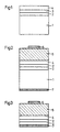
- the active layer 3 according to the exemplary embodiment according to FIG.
- the active layer 3 can also be formed by a homo-pn junction.
- the layer structure shown in FIG. 1 is particularly suitable for the production of particularly fast infrared-emitting luminescent diodes.
- the first Al x Ga 1-x As cladding layer 2 and the active layer 3 are produced by means of a MOVPE (metal organogas phase epitaxy) process, while the second Al x Ga 1-x As cladding layer 4 by means of an LPE (liquid phase epitaxy) - Process is manufactured.
- MOVPE metal organogas phase epitaxy
- LPE liquid phase epitaxy
- Reference numerals 6 and 7 denote electrically conductive electrode connections, which have been omitted from the illustration in FIG. 1 for the sake of simplicity.
- the Al x Ga 1-x As coupling-out layer 5 is designed as a self-supporting layer with a thickness of at least approximately 50 ⁇ m, and the optically absorbing substrate 1 is detached by etching or the like detaching step.
- the self-supporting decoupling layer 5 serves, as it were, as a transparent substrate, which supports the structure consisting of the layers 2, 3, 4 and 6, 7.
- inventions shown in Figures 2 and 3 are particularly suitable for producing particularly bright infrared emitters Luminescent diodes.
Landscapes
- Led Devices (AREA)
- Liquid Deposition Of Substances Of Which Semiconductor Devices Are Composed (AREA)
Description
- Figur 1
- eine schematische Schnittdarstellung einer IR-Lumineszenzdiode gemäß einem ersten Ausführungsbeispiel der Erfindung;
- Figur 2
- eine schematische Schnittdarstellung einer IR-Lumineszenzdiode gemäß einem zweiten Ausführungsbeispiel der Erfindung; und
- Figur 3
- eine schematische Schnittdarstellung einer IR-Lumineszenzdiode gemäß einem dritten Ausführungsbeispiel der Erfindung.
- 1
- Halbleitersubstrat
- 2
- erste AlxGa1-xAs-Mantelschicht
- 3
- aktive Schicht
- 4
- zweite AlxGa1-xAs-Mantelschicht
- 5
- AlxGa1-xAs-Auskopplungsschicht
- 6, 7
- elektrisch leitende Elektrodenanschlüsse
Claims (9)
- Verfahren zur Herstellung einer infrarotemittierenden Lumineszenzdiode, bei der auf einem Halbleitersubstrat (1), vorzugsweise bestehend aus GaAs, eine im Betrieb der Lumineszenzdiode eine Infrarot-Strahlung aussendende aktive Schichtenfolge aufgebracht wird, die ausgehend vom Halbleitersubstrat (1) eine erste AlGaAs-Mantelschicht (2), eine GaAs und/oder AlGaAs enthaltende aktive Schicht (3) und eine zweite AlGaAs-Mantelschicht (4) aufweist, wobei die erste AlGaAs-Mantelschicht (2) und die aktive Schicht (3) vermittels eines MOVPE-(Metallorganogasphasenepitaxie)-Verfahrens hergestellt werden, dadurch gekennzeichnet, dass die zweite AlGaAs-Mantelschicht (4) vermittels eines LPE(Flüssigphasenepitaxie) -Verfahrens hergestellt wird.
- Verfahren nach Anspruch 1, dadurch gekennzeichnet, dass die erste AlGaAs-Mantelschicht (2) und/oder die zweite AlGaAs-Mantelschicht (4) jeweils einen Al-Gehalt von 10 % bis 35 % aufweisen.
- Verfahren nach Anspruch 1 oder 2, dadurch gekennzeichnet, dass die Herstellung einer Vielzahl von infrarotemittierenden Lumineszenzdioden im Waferverbund erfolgt, wobei der Wafer einen Durchmesser von mehr als 5,08 cm (zwei Zoll) besitzt.
- Verfahren nach einem der Ansprüche 1 bis 3, dadurch gekennzeichnet, dass auf der zweiten AlGaAs-Mantelschicht (4) eine elektrisch leitfähige, im infraroten Spektralbereich optisch transparente Auskopplungsschicht (5) mit einer Dicke von wenigstens 10 µm vermittels einem LPE-(Flüssigphasenepitaxie)-Verfahren abgeschieden wird.
- Verfahren nach Anspruch 4, dadurch gekennzeichnet, dass die Auskopplungsschicht (5) selbsttragend ausgebildet wird und eine Dicke von wenigstens 50 µm besitzt.
- Verfahren nach Anspruch 5, dadurch gekennzeichnet, dass das vorzugsweise aus GaAs bestehende Halbleitersubstrat (1) nach Fertigung der selbsttragenden Auskopplungsschicht (5) abgelöst wird.
- Verfahren nach Anspruch 5 oder 6, dadurch gekennzeichnet, dass die Auskopplungsschicht (5) aus AlGaAs mit einem Al-Gehalt von vorzugsweise 20 % bis 35 % besteht.
- Verfahren nach einem der Ansprüche 5 bis 7, dadurch gekennzeichnet, dass die Auskopplungsschicht (5) in mehreren LPE-Einzelschritten gefertigt wird.
- Verfahren nach einem der Ansprüche 4 bis 8, dadurch gekennzeichnet, dass die Auskopplungsschicht (5) mittels eines Temperaturdifferenz-LPE-Verfahrens hergestellt wird.
Applications Claiming Priority (3)
| Application Number | Priority Date | Filing Date | Title |
|---|---|---|---|
| DE19631906 | 1996-08-07 | ||
| DE19631906 | 1996-08-07 | ||
| PCT/DE1997/001641 WO1998006133A2 (de) | 1996-08-07 | 1997-08-04 | Verfahren zur herstellung einer infrarotemittierenden lumineszenzdiode |
Publications (2)
| Publication Number | Publication Date |
|---|---|
| EP0917741A2 EP0917741A2 (de) | 1999-05-26 |
| EP0917741B1 true EP0917741B1 (de) | 2001-10-31 |
Family
ID=7802051
Family Applications (1)
| Application Number | Title | Priority Date | Filing Date |
|---|---|---|---|
| EP97936591A Expired - Lifetime EP0917741B1 (de) | 1996-08-07 | 1997-08-04 | Verfahren zur herstellung einer infrarotemittierenden lumineszenzdiode |
Country Status (6)
| Country | Link |
|---|---|
| US (1) | US6440765B1 (de) |
| EP (1) | EP0917741B1 (de) |
| JP (1) | JP2000516768A (de) |
| CN (1) | CN1227670A (de) |
| DE (1) | DE59705207D1 (de) |
| WO (1) | WO1998006133A2 (de) |
Families Citing this family (6)
| Publication number | Priority date | Publication date | Assignee | Title |
|---|---|---|---|---|
| JP2982010B2 (ja) * | 1989-06-23 | 1999-11-22 | 三菱電機株式会社 | 数値制御方法及び装置 |
| DE10056476B4 (de) * | 2000-11-15 | 2012-05-03 | Osram Opto Semiconductors Gmbh | Strahlungsemittierender Halbleiterkörper und Verfahren zu dessen Herstellung |
| DE10224219B4 (de) * | 2002-05-31 | 2010-05-27 | Osram Opto Semiconductors Gmbh | Lichtemittierendes Halbleiterbauelement mit zumindest teilweise voneinander getrennten Lichterzeugungs- und Lichtauskopplungsbereichen |
| US20040098793A1 (en) * | 2002-11-19 | 2004-05-27 | Gershenson Joel H. | Protective trauma device straps for helmets |
| WO2015008243A1 (en) * | 2013-07-19 | 2015-01-22 | Koninklijke Philips N.V. | Pc led with optical element and without substrate carrier |
| CN105870227B (zh) * | 2016-06-12 | 2017-07-14 | 天津三安光电有限公司 | 红外发光二极管 |
Family Cites Families (7)
| Publication number | Priority date | Publication date | Assignee | Title |
|---|---|---|---|---|
| JPS6055678A (ja) * | 1983-09-06 | 1985-03-30 | Nec Corp | 発光ダイオ−ド |
| JPH0770755B2 (ja) | 1988-01-21 | 1995-07-31 | 三菱化学株式会社 | 高輝度led用エピタキシャル基板及びその製造方法 |
| US5115286A (en) | 1988-08-26 | 1992-05-19 | Hewlett-Packard Company | Electro-optical device with inverted transparent substrate and method for making same |
| US5103271A (en) * | 1989-09-28 | 1992-04-07 | Kabushiki Kaisha Toshiba | Semiconductor light emitting device and method of fabricating the same |
| US5070510A (en) * | 1989-12-12 | 1991-12-03 | Sharp Kabushiki Kaisha | Semiconductor laser device |
| US5233204A (en) | 1992-01-10 | 1993-08-03 | Hewlett-Packard Company | Light-emitting diode with a thick transparent layer |
| US5869849A (en) * | 1995-10-05 | 1999-02-09 | Industry Technology Research Institute | Light-emitting diodes with high illumination |
-
1997
- 1997-08-04 WO PCT/DE1997/001641 patent/WO1998006133A2/de not_active Ceased
- 1997-08-04 JP JP10507482A patent/JP2000516768A/ja active Pending
- 1997-08-04 EP EP97936591A patent/EP0917741B1/de not_active Expired - Lifetime
- 1997-08-04 DE DE59705207T patent/DE59705207D1/de not_active Expired - Fee Related
- 1997-08-04 CN CN97197120A patent/CN1227670A/zh active Pending
-
1999
- 1999-02-08 US US09/246,747 patent/US6440765B1/en not_active Expired - Fee Related
Also Published As
| Publication number | Publication date |
|---|---|
| WO1998006133A3 (de) | 1998-04-30 |
| EP0917741A2 (de) | 1999-05-26 |
| DE59705207D1 (de) | 2001-12-06 |
| CN1227670A (zh) | 1999-09-01 |
| US6440765B1 (en) | 2002-08-27 |
| WO1998006133A2 (de) | 1998-02-12 |
| JP2000516768A (ja) | 2000-12-12 |
Similar Documents
| Publication | Publication Date | Title |
|---|---|---|
| DE69025842T2 (de) | Lichtemittierende Halbleitervorrichtung und Verfahren zu ihrer Herstellung | |
| DE10213395B4 (de) | Indiumgalliumnitrid-Glättungsstrukturen für III-Nitried-Anordnungen | |
| DE69533276T2 (de) | Lichtemittierende Halbleitervorrichtungen | |
| EP1875523B1 (de) | Nitridhalbleiter-bauelement und verfahren zu seiner herstellung | |
| EP0985235B1 (de) | Verfahren zur herstellung eines lichtemittierenden bauelementes | |
| DE69514375T2 (de) | Lichtemittierende diode mit einer aktiven schicht aus einer nitridverbindung der gruppe iii, mit vertikaler geometrie und längerer lebensdauer | |
| DE19913355B4 (de) | Integrierte opto-elektronische Schaltung mit ZnO-Schicht als Lichtwellenleiter | |
| DE69838313T2 (de) | Optoelektronische Halbleiteranordnung auf Basis einer Nitridverbindung der Gruppe III | |
| EP1145331B1 (de) | Strahlungsemittierende halbleitervorrichtung mit mehrfach-quantentopf-struktur | |
| DE19953609B4 (de) | Dickenanpassen von waferverbundenen AlxGayInzN-Strukturen durch Laserschmelzen | |
| DE69510129T2 (de) | Oberflächenemittierende lumineszente Halbleitervorrichtung | |
| EP2248235B1 (de) | Kantenemittierender halbleiterlaser und verfahren zur herstellung eines kantenemittierenden halbleiterlasers | |
| DE19715572A1 (de) | Verfahren zum Herstellen von epitaktischen Schichten eines Verbindungshalbleiters auf einkristallinem Silizium und daraus hergestellte Leuchtdiode | |
| DE19531762A1 (de) | Licht emittierende Halbleiterdiode | |
| DE102006008929A1 (de) | Nitridhalbleiter-Bauelement und Verfahren zu seiner Herstellung | |
| DE102011114670A1 (de) | Verfahren zur Herstellung eines optoelektronischen Halbleiterchips und optoelektronischer Halbleiterchip | |
| DE69635180T2 (de) | Lichtemittierende Halbleitervorrichtung | |
| EP0752165A1 (de) | Quantenschichtstruktur | |
| DE4130536A1 (de) | Laserdiode fuer sichtbares licht | |
| DE2702935A1 (de) | Licht emittierendes halbleiterelement | |
| WO1998006133A2 (de) | Verfahren zur herstellung einer infrarotemittierenden lumineszenzdiode | |
| DE69022890T2 (de) | Verfahren zur Herstellung einer heteroepitaxialen Struktur. | |
| DE19622704A1 (de) | Epitaxialwafer und Verfahren zu seiner Herstellung | |
| DE69330845T2 (de) | Methoden für das Wachstum von Verbindungshalbleiterschichten | |
| DE3880442T2 (de) | Epitaxiale scheibe. |
Legal Events
| Date | Code | Title | Description |
|---|---|---|---|
| PUAI | Public reference made under article 153(3) epc to a published international application that has entered the european phase |
Free format text: ORIGINAL CODE: 0009012 |
|
| 17P | Request for examination filed |
Effective date: 19990120 |
|
| AK | Designated contracting states |
Kind code of ref document: A2 Designated state(s): DE FR GB |
|
| GRAG | Despatch of communication of intention to grant |
Free format text: ORIGINAL CODE: EPIDOS AGRA |
|
| 17Q | First examination report despatched |
Effective date: 20001129 |
|
| RAP1 | Party data changed (applicant data changed or rights of an application transferred) |
Owner name: OSRAM OPTO SEMICONDUCTORS GMBH & CO. OHG |
|
| GRAG | Despatch of communication of intention to grant |
Free format text: ORIGINAL CODE: EPIDOS AGRA |
|
| GRAH | Despatch of communication of intention to grant a patent |
Free format text: ORIGINAL CODE: EPIDOS IGRA |
|
| GRAH | Despatch of communication of intention to grant a patent |
Free format text: ORIGINAL CODE: EPIDOS IGRA |
|
| GRAH | Despatch of communication of intention to grant a patent |
Free format text: ORIGINAL CODE: EPIDOS IGRA |
|
| GRAA | (expected) grant |
Free format text: ORIGINAL CODE: 0009210 |
|
| AK | Designated contracting states |
Kind code of ref document: B1 Designated state(s): DE FR GB |
|
| GBT | Gb: translation of ep patent filed (gb section 77(6)(a)/1977) |
Effective date: 20011031 |
|
| REF | Corresponds to: |
Ref document number: 59705207 Country of ref document: DE Date of ref document: 20011206 |
|
| REG | Reference to a national code |
Ref country code: GB Ref legal event code: IF02 |
|
| PGFP | Annual fee paid to national office [announced via postgrant information from national office to epo] |
Ref country code: GB Payment date: 20020808 Year of fee payment: 6 |
|
| PGFP | Annual fee paid to national office [announced via postgrant information from national office to epo] |
Ref country code: FR Payment date: 20020829 Year of fee payment: 6 |
|
| PLBE | No opposition filed within time limit |
Free format text: ORIGINAL CODE: 0009261 |
|
| STAA | Information on the status of an ep patent application or granted ep patent |
Free format text: STATUS: NO OPPOSITION FILED WITHIN TIME LIMIT |
|
| 26N | No opposition filed | ||
| PG25 | Lapsed in a contracting state [announced via postgrant information from national office to epo] |
Ref country code: GB Free format text: LAPSE BECAUSE OF NON-PAYMENT OF DUE FEES Effective date: 20030804 |
|
| GBPC | Gb: european patent ceased through non-payment of renewal fee |
Effective date: 20030804 |
|
| PG25 | Lapsed in a contracting state [announced via postgrant information from national office to epo] |
Ref country code: FR Free format text: LAPSE BECAUSE OF NON-PAYMENT OF DUE FEES Effective date: 20040430 |
|
| REG | Reference to a national code |
Ref country code: FR Ref legal event code: ST |
|
| PGFP | Annual fee paid to national office [announced via postgrant information from national office to epo] |
Ref country code: DE Payment date: 20071022 Year of fee payment: 11 |
|
| PG25 | Lapsed in a contracting state [announced via postgrant information from national office to epo] |
Ref country code: DE Free format text: LAPSE BECAUSE OF NON-PAYMENT OF DUE FEES Effective date: 20090303 |