EP0911665B1 - Lichtstrahl-Abtastsystem - Google Patents
Lichtstrahl-Abtastsystem Download PDFInfo
- Publication number
- EP0911665B1 EP0911665B1 EP98120117A EP98120117A EP0911665B1 EP 0911665 B1 EP0911665 B1 EP 0911665B1 EP 98120117 A EP98120117 A EP 98120117A EP 98120117 A EP98120117 A EP 98120117A EP 0911665 B1 EP0911665 B1 EP 0911665B1
- Authority
- EP
- European Patent Office
- Prior art keywords
- scanning
- optical system
- imaging optical
- light beam
- curvature
- Prior art date
- Legal status (The legal status is an assumption and is not a legal conclusion. Google has not performed a legal analysis and makes no representation as to the accuracy of the status listed.)
- Expired - Lifetime
Links
Images


Classifications
-
- G—PHYSICS
- G02—OPTICS
- G02B—OPTICAL ELEMENTS, SYSTEMS OR APPARATUS
- G02B13/00—Optical objectives specially designed for the purposes specified below
- G02B13/0005—Optical objectives specially designed for the purposes specified below having F-Theta characteristic
Definitions
- This invention relates to a light beam scanning system according to the preamble of claim 1.
- a light beam scanning system is employed in an image read-out system and an image recording system in order to scan a recording medium by a light beam for reading out or recording an image on the recording medium.
- the stimulable phosphor sheet is scanned by a stimulating light beam and light emitted from the stimulable phosphor sheet upon stimulation thereof is detected.
- a light beam scanning system there has been known those comprising a light source, a deflector such as a rotary polygonal mirror for deflecting the light beam emitted from the light source, and a scanning/imaging optical system which causes the light beam deflected by the deflector to form an image on the surface of a recording medium and scan the same and is provided with an optical element such as an f ⁇ lens for causing the light to scan the surface at a constant speed and correcting curvature of field.
- a deflector such as a rotary polygonal mirror for deflecting the light beam emitted from the light source
- a scanning/imaging optical system which causes the light beam deflected by the deflector to form an image on the surface of a recording medium and scan the same and is provided with an optical element such as an f ⁇ lens for causing the light to scan the surface at a constant speed and correcting curvature of field.
- An image is recorded on the recording medium or an image is read out from the recording medium by two-dimensionally scanning the surface of the recording medium by the light beam by causing the light beam to scan the surface at a constant speed in one direction (main scanning) while the recording medium is moved in a sub-scanning direction perpendicular to the main scanning direction.
- the light beam is collimated by a beam shaper and the collimated light beam is caused to scan the surface as disclosed, for instance, in Japanese Unexamined Patent Publication No. 2(1990)-115814, and in another type, the light beam is converged to form a beam spot on the surface and the beam spot is caused to scan the surface in order to suppress curvature of field as disclosed, for instance, in Japanese Unexamined Patent Publication No. 4(1992)-361218.
- the object of the present invention is to provide a light beam scanning system in which both the f ⁇ properties and the curvature of field can be accurately corrected.
- a light beam scanning system in accordance with the present invention comprises the features of claim 1.
- the light beam scanning system of the present invention be provided with a surface tilt correction optical system for correcting fluctuation in pitches on the surface to be scanned due to tilt of the deflecting surface of the deflector means.
- To correct distortion of an optical system is to cause the optical system to satisfy characteristics of f ⁇ tan ⁇ from definition of distortion.
- the relation between a scanning angle ⁇ and tan ⁇ is ⁇ tan ⁇ , which naturally gives a relation of f ⁇ f ⁇ tan ⁇ . Accordingly in order to effect f ⁇ correction, it is necessary to intentionally undercorrect distortion by f ⁇
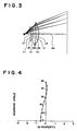
- a light beam scanning system in accordance with a first embodiment of the present invention comprises a light source 1, a diverging optical system 3 which diverges a light beam 2 emitted from the light source 1, a rotary polygonal mirror 5 which deflects the diverged light beam 2 toward a surface 4 to be scanned, a cylindrical lens 6 which is disposed upstream of the polygonal mirror 5 and forms an image of the light beam 2 on a deflecting surface of the polygonal mirror 5, a scanning/imaging optical system 7 which disposed downstream of the polygonal mirror 5 and forms an image of the light beam 2 on the surface 4 and a reflecting mirror 8 which reflects the light beam 2 toward the surface 4.
- the scanning/imaging optical system 7 consists of first and second f ⁇ lenses 7A and 7B.
- the light beam 2 emitted from the light source 1 is converted to a divergent light beam by the diverging optical system 3 and then is caused to form an image of a deflecting surface of the rotary polygonal mirror 5.
- the light beam 2 deflected by the polygonal mirror 5 travels through the scanning/imaging optical system 7 and is reflected by the reflecting mirror 8 to form an image on the surface 4.
- the image of the light beam 3 scans the surface 4 in the main scanning direction while the surface 4 is conveyed by a conveyor means (not shown) in a sub-scanning direction substantially perpendicular to the main scanning direction, whereby the light beam 2 two-dimensionally scans the entire surface 4.
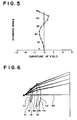
- a light beam scanning system in accordance with a second embodiment of the present invention will be described with reference to Figures 2A and 2B, hereinbelow.
- the light beam scanning system of the second embodiment differs from that of the first embodiment in that a cylindrical lens 7C having power in a direction perpendicular to the main scanning direction on the surface 4 is added to the scanning/imaging optical system 7 and a cylindrical mirror 9 is employed in place of the reflecting mirror 8.
- scanning/imaging optical systems which can be employed in the present invention will be described in comparison with a scanning/imaging optical system for comparison (will be referred to as "the comparative scanning/imaging optical system", hereinbelow) employed in a conventional light beam scanning system, hereinbelow.
- the comparative scanning/imaging optical system consists of first and second lens elements L1 and L2.
- the radii of curvature r (mm) of the faces of the lenses L1 and L2, the axial surface separations d (mm), glass materials, the diameter of the entrance pupil, the wavelength, half of the maximum scanning angle, the power distribution of the lenses and the performance of the scanning/imaging optical system are as shown in the following table 1.
- the subscripts attached to r and d represents the order of the faces of the lenses and the surface separations as numbered from the light source side.
- f all represents the composite focal length of the diverging optical system and the scanning/imaging optical system
- f GF represents the focal length of the diverging optical system
- r 1GR represents the radius of curvature of the first surface of the scanning/imaging optical system
- r 2GR represents the radius of curvature of the second surface of the scanning/imaging optical system
- r 4GR represents the radius of curvature of the fourth surface of the scanning/imaging optical system
- f GR1 represents the focal length of the first lens element L1
- f GR2 represents the focal length of the second lens element L2.
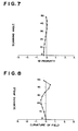
- ratio is a ratio of the scanning angle at the measuring point to the maximum scanning angle
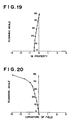
- curvature of field is astigmatism in the main scanning direction
- f ⁇ properties is a value obtained by dividing the difference between the position of an actual scanning spot on a scanning line and the position of a reference point by the position of the reference point.
- p-p is the difference between a maximum value and a minimum value of each of the curvature of field and the f ⁇ properties.
- a first specified example of the scanning/imaging optical system which can be employed in the light beam scanning system of the present invention where a divergent light beam is used is shown in Figure 6.
- the scanning/imaging optical system of the first specified example consists of first and second lens elements L1 and L2.
- the radii of curvature r (mm) of the faces of the lenses L1 and L2, the axial surface separations d (mm), glass materials, the diameter of the entrance pupil, the wavelength, half of the maximum scanning angle, the power distribution of the lenses and the performance of the scanning/imaging optical system are as shown in the following table 2.
- the scanning/imaging optical system of the first example satisfies the following formulae (1) to (3). -1.42 ⁇ f all /f GF ⁇ 0 r 1GR ⁇ 0, r 2GR ⁇ 0, r 4GR ⁇ 0 f GR1 >0, f GR2 >0
- a second specified example of the scanning/imaging optical system which can be employed in the light beam scanning system of the present invention where a divergent light beam is used is shown in Figure 9.
- the scanning/imaging optical system of the second specified example consists of first and second lens elements L1 and L2.
- the radii of curvature r (mm) of the faces of the lenses L1 and L2, the axial surface separations d (mm), glass materials, the diameter of the entrance pupil, the wavelength, half of the maximum scanning angle, the power distribution of the lenses and the performance of the scanning/imaging optical system are as shown in the following table 3.
- the scanning/imaging optical system of the first example satisfies the aforesaid formulae (1) to (3).
- a third specified example of the scanning/imaging optical system which can be employed in the light beam scanning system of the present invention where a divergent light beam is used is shown in Figure 12.
- the scanning/imaging optical system of the first specified example consists of first and second lens elements L1 and L2.
- the radii of curvature r (mm) of the faces of the lenses L1 and L2, the axial surface separations d (mm), glass materials, the diameter of the entrance pupil, the wavelength, half of the maximum scanning angle, the power distribution of the lenses and the performance of the scanning/imaging optical system are as shown in the following table 4.
- the scanning/imaging optical system of the first example satisfies the aforesaid formulae (1) to (3).
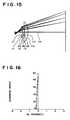
- a fourth specified example of the scanning/imaging optical system which can be employed in the light beam scanning system of the present invention where a divergent light beam is used is shown in Figure 15.
- the scanning/imaging optical system of the fourth specified example consists of first and second lens elements L1 and L2.
- the radii of curvature r (mm) of the faces of the lenses L1 and L2, the axial surface separations d (mm), glass materials, the diameter of the entrance pupil, the wavelength, half of the maximum scanning angle, the power distribution of the lenses and the performance of the scanning/imaging optical system are as shown in the following table 5.
- the scanning/imaging optical system of the fourth example satisfies the aforesaid formulae (1) to (3).
- a fifth specified example of the scanning/imaging optical system which can be employed in the light beam scanning system of the present invention where a divergent light beam is used is shown in Figure 18.
- the scanning/imaging optical system of the fifth specified example consists of first and second lens elements L1 and L2.
- the radii of curvature r (mm) of the faces of the lenses L1 and L2, the axial surface separations d (mm), glass materials, the diameter of the entrance pupil, the wavelength, half of the maximum scanning angle, the power distribution of the lenses and the performance of the scanning/imaging optical system are as shown in the following table 6.
- the scanning/imaging optical system of the fifth example satisfies the aforesaid formulae (2) and (3) but does not satisfy the aforesaid formula (1). Further the degree of divergence in the diverging optical system is larger than those in the first to fourth examples.
- a sixth specified example of the scanning/imaging optical system which can be employed in the light beam scanning system of the present invention where the cylindrical lens 7C and the cylindrical mirror 9 are employed to correct fluctuation in pitches on the surface 4 due to tilt of deflecting surfaces of the rotary polygonal mirror 5 as shown in Figure 2.
- the radii of curvature r (mm) of the faces of the lenses L1 and L2, the axial surface separations d (mm), glass materials, the diameter of the entrance pupil, the wavelength, half of the maximum scanning angle, the power distribution of the lenses and the performance of the scanning/imaging optical system are as shown in the following table 7.
- Table 7 also includes data on the cylindrical lenses 6 and 7C and the cylindrical mirror 9.
- the scanning/imaging optical system of the first example satisfies the aforesaid formulae (1) to (3).
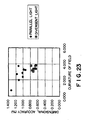
- Figure 23 is a view showing the relations between the curvature of field in the main scanning direction and the f ⁇ properties (accuracy in the dimensions of the image) for parallel light and divergent light, and
- Figure 23 shows the result of the comparison for parallel light and divergent light
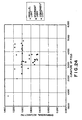
- Figure 24 shows the result of the comparison for parallel light, divergent light and convergent light.
- the light beam scanning systems employing a divergent light beam is superior to those employing a parallel light beam in the f ⁇ properties though equivalent or slightly inferior to the same in the curvature of field in the main scanning direction.
- the light beam scanning systems employing a divergent light beam is superior to those employing a convergent light beam both in the f ⁇ properties and the curvature of field in the main scanning direction.
- the light beam scanning system of the present invention may be variously modified without limited to the embodiments described above.
- the radii of curvature r of the lenses and the surface separations d may be variously changed.
Claims (2)
- Lichtstrahl-Abtastsystem, umfassend:dadurch gekennzeichnet, daß die Abtast-/Abbildungsoptik (7) aufweist: ein erstes und ein zweites Linsenelement (7A, 7B), die in dieser Reihenfolge ausgehend von der Lichtquellenseite angeordnet sind und eine erste bis vierte Oberfläche aufweisen, gezählt von der Seite der Lichtquelle aus, und außerdem folgende Formeln (1) bis (3) erfüllen:eine Strahlformereinrichtung (3), die einen von einer Lichtquelle (1) emittierten Lichtstrahl formt und eine Zerstreuungsoptik (3) aufweist, welche den Lichtstrahl in gestreutes Licht umwandelt;eine Ablenkeinrichtung (5), die den Lichtstrahl zum Abtasten einer Fläche (4) in einer Hauptabtastrichtung ablenkt, undeine Abtast-/Abbildungsoptik (7), die den von der Ablenkeinrichtung (5) abgelenkten Lichtstrahl veranlaßt, auf der Oberfläche (4) ein Bild zu erzeugen und dieses abzutasten,
- System nach Anspruch 1, weiterhin umfassend eine Oberflächenneigungs-Korrekturoptik (7C, 9) zum Korrigieren von Neigungsschwankungen auf der abzutastenden Oberfläche aufgrund der Neigung der Ablenkfläche der Ablenkeinrichtung (5).
Applications Claiming Priority (3)
| Application Number | Priority Date | Filing Date | Title |
|---|---|---|---|
| JP29268797A JP3433070B2 (ja) | 1997-10-24 | 1997-10-24 | 光ビーム走査装置 |
| JP292687/97 | 1997-10-24 | ||
| JP29268797 | 1997-10-24 |
Publications (3)
| Publication Number | Publication Date |
|---|---|
| EP0911665A2 EP0911665A2 (de) | 1999-04-28 |
| EP0911665A3 EP0911665A3 (de) | 2003-10-01 |
| EP0911665B1 true EP0911665B1 (de) | 2005-10-12 |
Family
ID=17785008
Family Applications (1)
| Application Number | Title | Priority Date | Filing Date |
|---|---|---|---|
| EP98120117A Expired - Lifetime EP0911665B1 (de) | 1997-10-24 | 1998-10-23 | Lichtstrahl-Abtastsystem |
Country Status (4)
| Country | Link |
|---|---|
| US (1) | US6195189B1 (de) |
| EP (1) | EP0911665B1 (de) |
| JP (1) | JP3433070B2 (de) |
| DE (1) | DE69831843T2 (de) |
Families Citing this family (16)
| Publication number | Priority date | Publication date | Assignee | Title |
|---|---|---|---|---|
| JP4949633B2 (ja) * | 2005-02-04 | 2012-06-13 | 株式会社リコー | 光走査装置及び画像形成装置 |
| JP4551332B2 (ja) * | 2006-01-11 | 2010-09-29 | Hoya株式会社 | 走査装置 |
| US8509140B2 (en) * | 2006-11-21 | 2013-08-13 | Honeywell International Inc. | System and method for transmitting information using aircraft as transmission relays |
| US8107412B2 (en) * | 2007-08-08 | 2012-01-31 | Honeywell International Inc. | Gatelink startup controlled by ACARS CMU |
| US7729263B2 (en) * | 2007-08-08 | 2010-06-01 | Honeywell International Inc. | Aircraft data link network routing |
| US7835734B2 (en) * | 2007-09-20 | 2010-11-16 | Honeywell International Inc. | System and method for wireless routing of data from an aircraft |
| US8811265B2 (en) * | 2007-10-19 | 2014-08-19 | Honeywell International Inc. | Ad-hoc secure communication networking based on formation flight technology |
| US9264126B2 (en) * | 2007-10-19 | 2016-02-16 | Honeywell International Inc. | Method to establish and maintain an aircraft ad-hoc communication network |
| US8570990B2 (en) * | 2007-12-04 | 2013-10-29 | Honeywell International Inc. | Travel characteristics-based ad-hoc communication network algorithm selection |
| US9467221B2 (en) * | 2008-02-04 | 2016-10-11 | Honeywell International Inc. | Use of alternate communication networks to complement an ad-hoc mobile node to mobile node communication network |
| US20090318138A1 (en) * | 2008-06-20 | 2009-12-24 | Honeywell International Inc. | System and method for in-flight wireless communication |
| US8190147B2 (en) * | 2008-06-20 | 2012-05-29 | Honeywell International Inc. | Internetworking air-to-air network and wireless network |
| WO2014103654A1 (ja) * | 2012-12-27 | 2014-07-03 | 富士フイルム株式会社 | 光ビーム走査装置および放射線画像読取装置 |
| JP2014235351A (ja) * | 2013-06-04 | 2014-12-15 | 富士フイルム株式会社 | 走査光学系、光走査装置および放射線画像読取装置 |
| JP2015102623A (ja) * | 2013-11-22 | 2015-06-04 | 富士フイルム株式会社 | 走査光学系、光走査装置および放射線画像読取装置 |
| DE102020202549B4 (de) | 2020-02-28 | 2022-05-05 | Trumpf Laser Gmbh | Optische Anordnung mit einem F-Theta-Objektiv |
Family Cites Families (8)
| Publication number | Priority date | Publication date | Assignee | Title |
|---|---|---|---|---|
| US3995110A (en) * | 1973-12-20 | 1976-11-30 | Xerox Corporation | Flying spot scanner with plural lens correction |
| US5005928A (en) * | 1988-07-15 | 1991-04-09 | Ricoh Company, Ltd. | Optical scanning system |
| JPH02115814A (ja) | 1988-10-25 | 1990-04-27 | Dainippon Screen Mfg Co Ltd | 光ビーム走査装置 |
| JP2999853B2 (ja) | 1991-06-10 | 2000-01-17 | 東芝テック株式会社 | 光走査装置 |
| JP3337510B2 (ja) * | 1992-07-22 | 2002-10-21 | 株式会社リコー | 光走査装置 |
| US5276544A (en) * | 1992-11-27 | 1994-01-04 | Xerox Corporation | Two element optical system for focus error correction in laser scanning systems |
| JP3330248B2 (ja) * | 1995-02-20 | 2002-09-30 | 松下電器産業株式会社 | 光走査装置、画像形成装置及び画像読み取り装置 |
| JP3679490B2 (ja) * | 1996-02-21 | 2005-08-03 | 富士ゼロックス株式会社 | 光学走査装置 |
-
1997
- 1997-10-24 JP JP29268797A patent/JP3433070B2/ja not_active Expired - Fee Related
-
1998
- 1998-10-23 EP EP98120117A patent/EP0911665B1/de not_active Expired - Lifetime
- 1998-10-23 DE DE69831843T patent/DE69831843T2/de not_active Expired - Lifetime
- 1998-10-26 US US09/178,641 patent/US6195189B1/en not_active Expired - Lifetime
Also Published As
| Publication number | Publication date |
|---|---|
| US6195189B1 (en) | 2001-02-27 |
| EP0911665A2 (de) | 1999-04-28 |
| DE69831843D1 (de) | 2006-02-23 |
| EP0911665A3 (de) | 2003-10-01 |
| JPH11125790A (ja) | 1999-05-11 |
| JP3433070B2 (ja) | 2003-08-04 |
| DE69831843T2 (de) | 2006-04-27 |
Similar Documents
| Publication | Publication Date | Title |
|---|---|---|
| EP0827004B1 (de) | Korrigiertes optisches Abtastgerät | |
| EP0911665B1 (de) | Lichtstrahl-Abtastsystem | |
| US7154651B2 (en) | Optical scanning device and imaging apparatus implementing the same | |
| US6222662B1 (en) | Optical scanning device and a scanning lens therefor | |
| US20030128413A1 (en) | Optical scanning system with unvarying image surface under environmental temperature change | |
| JPH0627904B2 (ja) | レーザービームの走査光学系 | |
| KR100384431B1 (ko) | 다중 비임 주사 광 시스템 및 이를 사용하는 화상 형성 장치 | |
| EP0360233A2 (de) | Telezentrisches f-Theta Linsensystem | |
| US5969877A (en) | Dual wavelength F-theta scan lens | |
| JP3567408B2 (ja) | 走査光学装置及び走査光学装置用の走査光学レンズ | |
| JP5269169B2 (ja) | 走査光学装置及びそれを有するレーザービームプリンタ | |
| US5940200A (en) | Scanning optical system | |
| US6670980B1 (en) | Light-scanning optical system | |
| US4586782A (en) | Laser beam optical system with inclined cylindrical lens | |
| EP1411380A2 (de) | Optische Abtastvorrichtung | |
| JP3121452B2 (ja) | 光走査装置 | |
| US6643044B1 (en) | Scanning optical system | |
| US6178030B1 (en) | Light-scanning optical system having wobble-correcting function and light-scanning apparatus using the same | |
| US5982523A (en) | Tilt correcting optical system | |
| JPH05127077A (ja) | シリンドリカルレンズ系 | |
| US6570696B2 (en) | Optical system for scanning and optical scanning apparatus | |
| US6466350B2 (en) | Scanning optical system | |
| JP3381333B2 (ja) | 光走査装置 | |
| JP3364525B2 (ja) | 走査結像レンズおよび光走査装置 | |
| US5757534A (en) | Light scanning optical system and apparatus using the same |
Legal Events
| Date | Code | Title | Description |
|---|---|---|---|
| PUAI | Public reference made under article 153(3) epc to a published international application that has entered the european phase |
Free format text: ORIGINAL CODE: 0009012 |
|
| AK | Designated contracting states |
Kind code of ref document: A2 Designated state(s): AT BE CH CY DE DK ES FI FR GB GR IE IT LI LU MC NL PT SE |
|
| AX | Request for extension of the european patent |
Free format text: AL;LT;LV;MK;RO;SI |
|
| PUAL | Search report despatched |
Free format text: ORIGINAL CODE: 0009013 |
|
| AK | Designated contracting states |
Kind code of ref document: A3 Designated state(s): AT BE CH CY DE DK ES FI FR GB GR IE IT LI LU MC NL PT SE |
|
| AX | Request for extension of the european patent |
Extension state: AL LT LV MK RO SI |
|
| RIC1 | Information provided on ipc code assigned before grant |
Ipc: 7G 02B 27/00 B Ipc: 7G 02B 26/12 B Ipc: 7G 02B 13/00 A |
|
| 17P | Request for examination filed |
Effective date: 20040325 |
|
| 17Q | First examination report despatched |
Effective date: 20040426 |
|
| AKX | Designation fees paid |
Designated state(s): DE FR NL |
|
| GRAP | Despatch of communication of intention to grant a patent |
Free format text: ORIGINAL CODE: EPIDOSNIGR1 |
|
| GRAS | Grant fee paid |
Free format text: ORIGINAL CODE: EPIDOSNIGR3 |
|
| GRAA | (expected) grant |
Free format text: ORIGINAL CODE: 0009210 |
|
| AK | Designated contracting states |
Kind code of ref document: B1 Designated state(s): DE FR NL |
|
| REF | Corresponds to: |
Ref document number: 69831843 Country of ref document: DE Date of ref document: 20060223 Kind code of ref document: P |
|
| ET | Fr: translation filed | ||
| PLBE | No opposition filed within time limit |
Free format text: ORIGINAL CODE: 0009261 |
|
| STAA | Information on the status of an ep patent application or granted ep patent |
Free format text: STATUS: NO OPPOSITION FILED WITHIN TIME LIMIT |
|
| 26N | No opposition filed |
Effective date: 20060713 |
|
| REG | Reference to a national code |
Ref country code: FR Ref legal event code: TP Ref country code: FR Ref legal event code: CD |
|
| PGFP | Annual fee paid to national office [announced via postgrant information from national office to epo] |
Ref country code: FR Payment date: 20121018 Year of fee payment: 15 Ref country code: DE Payment date: 20121017 Year of fee payment: 15 |
|
| PGFP | Annual fee paid to national office [announced via postgrant information from national office to epo] |
Ref country code: NL Payment date: 20121016 Year of fee payment: 15 |
|
| REG | Reference to a national code |
Ref country code: NL Ref legal event code: V1 Effective date: 20140501 |
|
| REG | Reference to a national code |
Ref country code: DE Ref legal event code: R119 Ref document number: 69831843 Country of ref document: DE Effective date: 20140501 |
|
| REG | Reference to a national code |
Ref country code: FR Ref legal event code: ST Effective date: 20140630 |
|
| PG25 | Lapsed in a contracting state [announced via postgrant information from national office to epo] |
Ref country code: FR Free format text: LAPSE BECAUSE OF NON-PAYMENT OF DUE FEES Effective date: 20131031 Ref country code: DE Free format text: LAPSE BECAUSE OF NON-PAYMENT OF DUE FEES Effective date: 20140501 Ref country code: NL Free format text: LAPSE BECAUSE OF NON-PAYMENT OF DUE FEES Effective date: 20140501 |