EP0905287A2 - Verfahren und Vorrichtung zur Herstellung eines epitaktischen Wafers aus Verbindungshalbleitern durch Dampfphasenwachstum - Google Patents
Verfahren und Vorrichtung zur Herstellung eines epitaktischen Wafers aus Verbindungshalbleitern durch Dampfphasenwachstum Download PDFInfo
- Publication number
- EP0905287A2 EP0905287A2 EP98306285A EP98306285A EP0905287A2 EP 0905287 A2 EP0905287 A2 EP 0905287A2 EP 98306285 A EP98306285 A EP 98306285A EP 98306285 A EP98306285 A EP 98306285A EP 0905287 A2 EP0905287 A2 EP 0905287A2
- Authority
- EP
- European Patent Office
- Prior art keywords
- compound semiconductor
- source gas
- gas
- group
- semiconductor wafers
- Prior art date
- Legal status (The legal status is an assumption and is not a legal conclusion. Google has not performed a legal analysis and makes no representation as to the accuracy of the status listed.)
- Withdrawn
Links
- 150000001875 compounds Chemical class 0.000 title claims abstract description 97
- 239000004065 semiconductor Substances 0.000 title claims abstract description 97
- 238000000034 method Methods 0.000 title claims abstract description 23
- 238000001947 vapour-phase growth Methods 0.000 title claims abstract description 19
- 235000012431 wafers Nutrition 0.000 claims abstract description 114
- 238000006243 chemical reaction Methods 0.000 claims abstract description 39
- 230000000737 periodic effect Effects 0.000 claims description 7
- 238000009826 distribution Methods 0.000 abstract description 7
- 239000007789 gas Substances 0.000 description 149
- JBRZTFJDHDCESZ-UHFFFAOYSA-N AsGa Chemical compound [As]#[Ga] JBRZTFJDHDCESZ-UHFFFAOYSA-N 0.000 description 29
- 229910001218 Gallium arsenide Inorganic materials 0.000 description 29
- 229910005540 GaP Inorganic materials 0.000 description 26
- XYFCBTPGUUZFHI-UHFFFAOYSA-N Phosphine Chemical compound P XYFCBTPGUUZFHI-UHFFFAOYSA-N 0.000 description 24
- 229910045601 alloy Inorganic materials 0.000 description 22
- 239000000956 alloy Substances 0.000 description 22
- 239000000203 mixture Substances 0.000 description 22
- 229910000073 phosphorus hydride Inorganic materials 0.000 description 16
- 239000000758 substrate Substances 0.000 description 13
- RBFQJDQYXXHULB-UHFFFAOYSA-N arsane Chemical compound [AsH3] RBFQJDQYXXHULB-UHFFFAOYSA-N 0.000 description 12
- HZXMRANICFIONG-UHFFFAOYSA-N gallium phosphide Chemical compound [Ga]#P HZXMRANICFIONG-UHFFFAOYSA-N 0.000 description 12
- 239000001257 hydrogen Substances 0.000 description 8
- 229910052739 hydrogen Inorganic materials 0.000 description 8
- 125000004435 hydrogen atom Chemical class [H]* 0.000 description 8
- XOYLJNJLGBYDTH-UHFFFAOYSA-M chlorogallium Chemical compound [Ga]Cl XOYLJNJLGBYDTH-UHFFFAOYSA-M 0.000 description 7
- UPWPDUACHOATKO-UHFFFAOYSA-K gallium trichloride Chemical compound Cl[Ga](Cl)Cl UPWPDUACHOATKO-UHFFFAOYSA-K 0.000 description 7
- IJGRMHOSHXDMSA-UHFFFAOYSA-N Atomic nitrogen Chemical compound N#N IJGRMHOSHXDMSA-UHFFFAOYSA-N 0.000 description 6
- 229910000070 arsenic hydride Inorganic materials 0.000 description 6
- 239000012159 carrier gas Substances 0.000 description 6
- 238000011144 upstream manufacturing Methods 0.000 description 6
- 230000003247 decreasing effect Effects 0.000 description 3
- 238000004519 manufacturing process Methods 0.000 description 3
- 229910052757 nitrogen Inorganic materials 0.000 description 3
- XKRFYHLGVUSROY-UHFFFAOYSA-N Argon Chemical compound [Ar] XKRFYHLGVUSROY-UHFFFAOYSA-N 0.000 description 2
- 239000007795 chemical reaction product Substances 0.000 description 2
- 238000013461 design Methods 0.000 description 2
- 239000012530 fluid Substances 0.000 description 2
- 238000005755 formation reaction Methods 0.000 description 2
- QJGQUHMNIGDVPM-UHFFFAOYSA-N nitrogen group Chemical group [N] QJGQUHMNIGDVPM-UHFFFAOYSA-N 0.000 description 2
- 238000005424 photoluminescence Methods 0.000 description 2
- 239000012808 vapor phase Substances 0.000 description 2
- RWSOTUBLDIXVET-UHFFFAOYSA-N Dihydrogen sulfide Chemical compound S RWSOTUBLDIXVET-UHFFFAOYSA-N 0.000 description 1
- GYHNNYVSQQEPJS-UHFFFAOYSA-N Gallium Chemical compound [Ga] GYHNNYVSQQEPJS-UHFFFAOYSA-N 0.000 description 1
- NINIDFKCEFEMDL-UHFFFAOYSA-N Sulfur Chemical compound [S] NINIDFKCEFEMDL-UHFFFAOYSA-N 0.000 description 1
- 229910052786 argon Inorganic materials 0.000 description 1
- 230000015572 biosynthetic process Effects 0.000 description 1
- 230000000052 comparative effect Effects 0.000 description 1
- 239000013078 crystal Substances 0.000 description 1
- 230000007547 defect Effects 0.000 description 1
- 238000011156 evaluation Methods 0.000 description 1
- 238000002474 experimental method Methods 0.000 description 1
- 229910052733 gallium Inorganic materials 0.000 description 1
- IXCSERBJSXMMFS-UHFFFAOYSA-N hcl hcl Chemical compound Cl.Cl IXCSERBJSXMMFS-UHFFFAOYSA-N 0.000 description 1
- 238000005259 measurement Methods 0.000 description 1
- 238000010926 purge Methods 0.000 description 1
- 229910052717 sulfur Inorganic materials 0.000 description 1
- 239000011593 sulfur Substances 0.000 description 1
Images

Classifications
-
- C—CHEMISTRY; METALLURGY
- C30—CRYSTAL GROWTH
- C30B—SINGLE-CRYSTAL GROWTH; UNIDIRECTIONAL SOLIDIFICATION OF EUTECTIC MATERIAL OR UNIDIRECTIONAL DEMIXING OF EUTECTOID MATERIAL; REFINING BY ZONE-MELTING OF MATERIAL; PRODUCTION OF A HOMOGENEOUS POLYCRYSTALLINE MATERIAL WITH DEFINED STRUCTURE; SINGLE CRYSTALS OR HOMOGENEOUS POLYCRYSTALLINE MATERIAL WITH DEFINED STRUCTURE; AFTER-TREATMENT OF SINGLE CRYSTALS OR A HOMOGENEOUS POLYCRYSTALLINE MATERIAL WITH DEFINED STRUCTURE; APPARATUS THEREFOR
- C30B25/00—Single-crystal growth by chemical reaction of reactive gases, e.g. chemical vapour-deposition growth
- C30B25/02—Epitaxial-layer growth
- C30B25/14—Feed and outlet means for the gases; Modifying the flow of the reactive gases
-
- C—CHEMISTRY; METALLURGY
- C30—CRYSTAL GROWTH
- C30B—SINGLE-CRYSTAL GROWTH; UNIDIRECTIONAL SOLIDIFICATION OF EUTECTIC MATERIAL OR UNIDIRECTIONAL DEMIXING OF EUTECTOID MATERIAL; REFINING BY ZONE-MELTING OF MATERIAL; PRODUCTION OF A HOMOGENEOUS POLYCRYSTALLINE MATERIAL WITH DEFINED STRUCTURE; SINGLE CRYSTALS OR HOMOGENEOUS POLYCRYSTALLINE MATERIAL WITH DEFINED STRUCTURE; AFTER-TREATMENT OF SINGLE CRYSTALS OR A HOMOGENEOUS POLYCRYSTALLINE MATERIAL WITH DEFINED STRUCTURE; APPARATUS THEREFOR
- C30B29/00—Single crystals or homogeneous polycrystalline material with defined structure characterised by the material or by their shape
- C30B29/10—Inorganic compounds or compositions
- C30B29/40—AIIIBV compounds wherein A is B, Al, Ga, In or Tl and B is N, P, As, Sb or Bi
Definitions
- This invention relates to a method for fabricating a compound semiconductor epitaxial wafer and a vapor phase growth apparatus using the method. More particularly, the present invention concerns a method for fabricating a compound semiconductor epitaxial wafer which is composed of elements belonging to a periodic table groups III and V and suitably used for fabrication of a light emitting diode, and a vapor phase growth apparatus using the method.
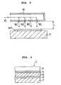
- a compound semiconductor epitaxial wafer in which an epitaxial layer of gallium arsenide phosphide GaAs 1-a P a (where a is a real number satisfying a relationship of 0 ⁇ a ⁇ 1) having constant alloy compositions (1-a) and a of gallium arsenide GaAs and gallium phosphide GaP respectively is formed on a single-crystalline substrate of gallium phosphide GaP or gallium arsenide GaAs.
- the emitted light wavelength of the light emitting diode is determined by the alloy composition a , which is 0.9 for the yellow-color light emitting diode, 0.65 for the orange-color diode and 0.57 for the red-color diode.
- a compound semiconductor epitaxial wafer 1 having such an epitaxial layer of the gallium arsenide phosphide GaAs 1-a P a as mentioned above is, as shown in Fig. 3, made up of a single-crystalline substrate 2 of, e.g., n type gallium phosphide GaP, an n type gallium phosphide GaP epitaxial layer 3, an alloy composition gradient layer 4 of n type gallium arsenide phosphide GaAs 1-x P x (0 ⁇ x ⁇ 1) having an alloy composition (1-x) of gallium arsenide GaAs varies in the growth direction of the epitaxial layer, an alloy composition constant layer 5 of gallium arsenide phosphide GaAs 1-a P a (0 ⁇ a ⁇ 1) having a constant alloy composition (1-a) of gallium arsenide GaAs, and an alloy composition constant layer 6 of n type gallium arsenide phosphide GaAs 1-a P a having a constant alloy composition (1-a
- gallium arsenide phosphide GaAs 1-x P x alloy composition gradient layer 4 gallium arsenide phosphide GaAs 1-a P a alloy composition constant layer 5
- gallium arsenide phosphide GaAs 1-a P a alloy composition constant layer 6 doped with nitrogen N will sometimes be generally referred to as the gallium arsenide phosphide GaAsP layers.
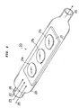
- compound semiconductor wafers 21a, 21b and 21c are placed on a wafer holder 27 disposed inside a reaction furnace 29 so that the reaction furnace 29 is heated by a heater (not shown) located outside the reaction furnace 29 while a hydrogen H 2 gas as a carrier gas 22 is introduced into the reaction furnace 29.
- a group III source gas 23 containing gallium chloride GaCl Collectively supplied together with the carrier gas 22 from a gas inlet 24 at one end of the reaction furnace 29 to a gas outlet 26 at the other end thereof are a group III source gas 23 containing gallium chloride GaCl, and a group V source gas 25 containing phosphine PH 3 and/or arsine AsH 3 .
- the group III source gas 23 and group V source gas 25 react with each other on the compound semiconductor wafers 21a, 21b and 21c to grow epitaxial layers.
- the above vapor phase epitaxial growth method has a defect that, since the group III source gas 23 and group V source gas 25 are collectively supplied from one end of the reaction furnace 29, the epitaxial layer formed as grown on the wafer placed closer to the upstream side is thicker and the epitaxial layer on the wafer placed closer to the downstream side is thinner, because the downstream side has less source gases.
- the group III source gas 23 and group V source gas 25 react on the side closer to the gas inlet 24 with the result that a relatively large amount of reaction product deposits on the upstream-side wafer; whereas, the residual source gases react on the side closer to the gas outlet 26 with the result that a relatively small amount of reaction product deposits on the downstream-side wafer.
- the thickness of the epitaxial layer greatly varies between the upstream and downstream wafers, and the maximum of the variation sometimes reaches 3 or 4 times the minimum of the variation in the reaction furnace.
- the thickness of the epitaxial layer is associated with characteristics of emitted light wavelength, luminance, forward voltage, etc., variations in the thickness of the epitaxial layer will cause variations in the above quality characteristics.
- the above object is attained by providing a method for fabricating a compound semiconductor epitaxial wafer wherein a periodic table group III source gas and a periodic table group V source gas are supplied into a reaction furnace of a vapor phase growth apparatus to epitaxially grow a compound semiconductor film on main surfaces of a plurality of compound semiconductor wafers arranged within the reaction furnace.
- the group III source gas is flowed from one end of the reaction furnace to the other end thereof in such a manner that a flow path of the group III source gas is established along an array direction of the plurality of compound semiconductor wafers.
- the group V source gas is supplied as dispersedly from a plurality of locations at halfway of the flow path of the group III source gas.
- the gas supply step is carried out by directing the group V source gas toward the compound semiconductor wafers from their vicinities.
- the group V source gas be supplied from positions opposed to the compound semiconductor wafers.
- the supply positions of the group V source gas are set, from the viewpoint of causing a sufficient amount of group V source gas to reach the wafer surfaces, so that a vertical distance between the supply positions and the main surfaces of the compound semiconductor wafers is preferably not smaller than 1 mm and not larger than 20 mm.
- a vertical distance between the supply positions and the main surfaces of the compound semiconductor wafers is preferably not smaller than 1 mm and not larger than 20 mm.
- the amount of the group III source gas to be supplied be made excessive with respect to the amount of the group V source gas to be supplied. This is because, in the above case, the formation reaction of the compound semiconductor film will be supply-controlled with regard to the group V source gas, so that, so long as only the group V source gas is uniformly supplied from a plurality of locations, a uniform amount of compound semiconductor is formed at any position and thus a uniform thickness of compound semiconductor film can be formed on the wafers.
- a vapor phase growth apparatus for fabricating such a compound semiconductor epitaxial wafer comprises a reaction furnace, a wafer holder for holding the plurality of compound semiconductor wafers along a longitudinal direction of the reaction furnace therewithin, a first gas supply member for supplying the group III source gas from one end of the reaction furnace to the other end thereof in the furnace longitudinal direction, and a second gas supply member for dispersedly supplying the group V source gas from a plurality of gas discharge ports made open along a flow path of the group III source gas.
- the gas discharge ports of the second gas supply member be made open as directed toward the compound semiconductor wafers in the vicinities thereof.
- the gas discharge ports are made open preferably as opposed to the main surfaces.
- opening faces of the gas discharge ports of the group V source gas be positioned so that a vertical distance between the main surfaces of the compound semiconductor wafers and the gas discharge ports is not smaller than 1mm and not larger than 20 mm.
- the second gas supply member are made so that a total opening area of the gas discharge ports per one of the compound semiconductor wafers is preferably increased as it goes toward a downstream side of the flow path of the group III source gas. This is because the group V source gas per se flowing through the second gas supply member becomes hard to flow as it goes toward the end due to its fluid resistance, which is corrected by increasing the total opening area of the gas discharge ports so that a uniform amount of group V source gas can be supplied at any supply location.
- the opening diameter of the ports in the downstream side should be made larger.
- the opening diameter is relatively small and the number of gas discharge ports having an identical opening diameter is varied depending on each location, its design can be facilitated and fine adjustment of the amount of gas to be supplied can be realized.
- FIG. 1 schematically shows a structure of a vapor phase growth apparatus 10 in accordance with an embodiment of the present invention
- Fig. 2 is an enlarged cross-sectional view of a gas outlet in Fig. 1.
- the vapor phase growth apparatus 10 of the present invention incorporate a reaction furnace 19 having a gas inlet 14 and a gas outlet 16. Supplied from the gas inlet 14 through a first gas supply tube 11 toward the gas outlet 16 at the other end of the tube are a hydrogen H 2 as a carrier gas 12 and a group III source gas 13 containing gallium chloride GaCl. That is, a flow path of the group III source gas 13 is established from the gas inlet 14 to the gas outlet 16.
- a wafer holder 17 on which compound semiconductor wafers W1, W2 and W3 are placed.
- the compound semiconductor wafers W1, W2 and W3 are arranged in a row along the flow path of the group III source gas 13 so that major surfaces of the wafers are parallel to the flow path.
- three wafers have been arranged in a row in Fig. 1, the numbers of such wafers and row are not limited to the specific example.
- the reaction furnace 19 also incorporates a second gas supply tube 18 which extends along the inner wall of the furnace from the gas inlet 14 to the gas outlet 16. Supplied into the second gas supply tube 18 is a group V source gas 15 which contains phosphine PH 3 and/or arsine AsH 3 .
- the second gas supply tube 18 is provided at its three side locations with gas discharge ports 18a, 18b and 18c which are opposed to the main surfaces of the compound semiconductor wafers W1, W2 and W3 respectively to discharge the group V source gas in a direction perpendicular to the main surfaces of the wafers.
- the respective numbers of gas discharge ports 18a, 18b and 18c corresponding to the compound semiconductor wafers W1, W2 and W3 are set to be increased as it goes from the upstream side of the flow path of the group III source gas 13 to the downstream side thereof.
- the gas discharge ports are all circular and has a diameter of 0.3 to 4 mm.
- the number of gas discharge ports 18a corresponding to the compound semiconductor wafer W1 is set to be two
- the number of gas discharge ports 18b corresponding to the compound semiconductor wafer W2 is set to be three
- the number of gas discharge ports 18c corresponding to the compound semiconductor wafer W3 is set to be four.
- a total opening area of the gas outlet ports for the compound semiconductor wafer W1 is set to be minimum
- a total opening area for the compound semiconductor wafer W3 is to be maximum.
- the respective total opening areas for the gas discharge ports are changed depending on the associated wafers. This is because, due to the fluid resistance of the interior of the second gas supply tube 18, the group V source gas flows more easily on the upstream side of the interior of the second gas supply tube 18 and flows less easily on the downstream side, so that the number of discharge ports for the downstream wafer is made larger than that for the upstream wafer to thereby supply a uniform amount of group V source gas 15 to the wafers.
- linear velocity of the discharged group V source gas 15 is large on the upstream side and small on the downstream side.
- linear velocity as used herein is expressed by a division of the gas flow rate per unit time by its cross-sectional area and in units of, e.g., cm/min.
- the flowability of the group V source gas 15 has been controlled by adjusting the numbers of such ports in the respective groups as an example in Fig. 1, the flowability adjustment may be effected by adjusting the size of each port or by selecting combinations of the port number and size. In either case, the total opening area of the gas discharge port group located on the uppermost-stream side of the flow path of the group III source gas 13 should be minimum, while the total opening area of the gas discharge port group located on the lowermost-stream side thereof should be maximum.
- a vertical distance L between the gas discharge ports 18a, 18b, 18c and compound semiconductor wafers W1, W2, W3 is set to be 1 to 20 mm.
- the gas discharge ports 18a, 18b or 18c are undesirably contacted with the compound semiconductor wafers W1, W2 or W3.
- the group V source gas 15 is flowed away by the group III source gas 13, for which reason the film thickness distribution of the GaAsP compound semiconductor film becomes worse and the GaAsP compound semiconductor film tends to deposit on the gas discharge ports 18a, 18b and 18c.
- the thickness of the epitaxial layer varies depending also on a temperature distribution in the interior of the reaction furnace 19.
- the compound semiconductor wafers W1, W2 and W3 placed within the reaction furnace 19 are heated by a heater (not shown) located outside the reaction furnace 19 while the carrier gas 12 is introduced into the reaction furnace 19.
- the group III source gas 13 which contains gallium chloride GaCl.
- the group V source gas 15 supplied from the gas discharge ports 18a, 18b and 18c of the second gas supply tube 18 is the group V source gas 15 as dispersively directed toward the associated opposing compound semiconductor wafers W1, W2 and W3.
- the group V source gas 15 When the group V source gas 15 is fed through the second gas supply tube 18 as dispersed into the vicinities of the compound semiconductor wafers W1, W2 and W3; the group V source gas will not react with the group III source gas before the group V source gas is discharged from the second gas supply tube 18, an identical concentration of the group V source gas can be fed into the vicinities of the compound semiconductor wafers W1, W2 and W3.
- the group V source gas 15 can reliably reach the compound semiconductor wafers W1, W2 and W3 spaced by the vertical distance L from the respectively opposing gas discharge ports 18a, 18b and 18c and can be brought into efficient contact with the group III source gas 13, thereby advancing its vapor phase growth smoothly.
- the gallium chloride GaCl as the group III source gas is excessively fed from the gas inlet 14 and when the group V source gas 15 containing the phosphine PH 3 and arsine AsH 3 is fed dispersively in the vicinities of the respective compound semiconductor wafers W1, W2 and W3 by an amount necessary for formation of a desired layer thickness, there can be formed an epitaxial layer which has a uniform thickness on each of the wafers.
- Such a vapor phase growth apparatus 10 as shown in Fig. 1 was used to form such a compound semiconductor epitaxial wafer 1 shown in Fig. 3.
- Each of the gallium phosphide GaP single-crystalline substrates is an n type substrate which is mirror-polished, has a thickness of about 300 ⁇ m, a diameter of 50 mm, a crystal orientation of (100) and an off angle of 10 degrees.
- the gas discharge ports 18a, 18b and 18c were set to have each a diameter of 2 mm, and the vertical distance between the gas discharge ports and wafers W1, W2 and W3 was set at 7 mm.
- a nitrogen N 2 gas was introduced into the reaction furnace 19 to sufficiently purge the air, after which a hydrogen H 2 as the carrier gas was introduced into the reaction furnace 19 at a flow rate of 3640 cm 3 /minute to displace the atmosphere, and then a temperature within the furnace was started to increase.
- a high-purity hydrogen chloride HCl was introduced into the furnace 19 at a flow rate of 140 cm 3 /minute to react with high-purity gallium Ga (not shown) within the reaction furnace and to generate a gallium chloride GaCl 13 gas as a group III source gas 13.
- phosphine PH 3 diluted into 10% with hydrogen H 2 as the group V source gas 15 as well as hydrogen sulfide H 2 S 50 ppm-diluted with hydrogen H 2 were both fed into the second gas supply tube 18 at flow rates of 700 cm 3 /minute and 190 cm 3 /minute, respectively, and then discharged from the gas discharge ports 18a, 18b and 18c toward the respectively opposing compound semiconductor wafers W1, W2 and W3 in a direction perpendicular thereto.
- Epitaxial layers to be next grown are doped with sulfur S and are all of an n type.
- the flow rate of the phosphine PH 3 diluted into 10% with hydrogen H 2 was gradually decreased from 700 cm 3 /minute to 455 cm 3 /minute and at the same time, the flow rate of arsine AsH 3 diluted into 10% with hydrogen H 2 was gradually increased from 0 cm 3 /minute to 245 cm 3 /minute. Further, the wafer temperature was decreased gradually from 845°C to 810°C.
- a total thickness of the epitaxial layers 3, 4, 5 and 6 thus formed on the gallium phosphide GaP single-crystalline substrate was measured.
- its maximum thickness was 42.0 ⁇ m in the center of the epitaxial layer on the compound semiconductor wafer W1
- its minimum was 33.6 ⁇ m in the lowermost stream part of the epitaxial layer formed on the compound semiconductor wafer W3. That is, variations in the layer thickness in the same lot was as very small as 1.25 times when expressed in terms of a magnification of the maximum to the minimum.
- a wavelength of emitted light of the compound semiconductor epitaxial wafer 1 is determined by the alloy composition a of the alloy composition constant layer 6 of the n type gallium arsenide phosphide GaAs 1-a P a doped with nitrogen N. Whether to obtain a design wavelength of emitted light is one of important characters as well as the layer thickness distribution and luminous intensity of the epitaxial layer.
- the compound semiconductor epitaxial wafer 1 fabricated according to the present example was subjected to evaluation of its light emission characteristics by the photoluminescence method.
- an argon laser having a wavelength of 514.5 nm was irradiated on the main surface of the compound semiconductor epitaxial wafer 1. This causes the wafer 1 to absorb the irradiated laser beam and at the same time, to emit photoluminescent light having a wavelength corresponding to the alloy composition a of the alloy composition constant layer 6 of the gallium arsenide phosphide GaAs 1-a P a formed on the wafer main surface.
- a wavelength ⁇ p where the intensity of the photoluminescent light becomes maximum was measured.
- Such a compound semiconductor epitaxial wafer 1 as shown in Fig. 3 was formed substantially in the same manner as in Example 1, except that such a prior art vapor phase growth apparatus 20 as shown in Fig. 4 was used.
- the wavelength ⁇ p of the emitted light was measured by the photoluminescence method, a longest value of 631 nm and a shortest value of 623 nm were observed for the compound semiconductor epitaxial wafers formed on the gallium phosphide GaP single-crystalline substrates 21a and 21c, respectively. That is, a variation in the wavelength was as large as 8 nm.
- the present invention has been explained in connection with the specific example, the present invention is not limited to the specific example.
- the present invention can be similarly applied not only to such a horizontal vapor phase growth apparatus as shown in Fig. 1 but also to a vertical barrel type apparatus.
- the thicknesses, alloy compositions and epitaxial growth conditions of the respective epitaxial layers may be suitably modified, selected and combined as necessary.
- the thickness of the epitaxial films can be effectively controlled. Thereby there can be obtained a uniform thickness of epitaxial layers independently of the arrangement of the wafers within the reaction furnace.
- the epitaxial wafers thus obtained can provide a uniform wavelength distribution when used for fabrication of, e.g., light emitting diodes, thus finding industrially highly useful applications.
Landscapes
- Chemical & Material Sciences (AREA)
- Engineering & Computer Science (AREA)
- Crystallography & Structural Chemistry (AREA)
- Materials Engineering (AREA)
- Metallurgy (AREA)
- Organic Chemistry (AREA)
- Chemical Kinetics & Catalysis (AREA)
- General Chemical & Material Sciences (AREA)
- Inorganic Chemistry (AREA)
- Crystals, And After-Treatments Of Crystals (AREA)
- Led Devices (AREA)
- Chemical Vapour Deposition (AREA)
Applications Claiming Priority (3)
| Application Number | Priority Date | Filing Date | Title |
|---|---|---|---|
| JP22570097A JPH1154442A (ja) | 1997-08-07 | 1997-08-07 | 化合物半導体エピタキシャルウェーハの製造方法およびこれに用いる気相成長装置 |
| JP225700/97 | 1997-08-07 | ||
| JP22570097 | 1997-08-07 |
Publications (2)
| Publication Number | Publication Date |
|---|---|
| EP0905287A2 true EP0905287A2 (de) | 1999-03-31 |
| EP0905287A3 EP0905287A3 (de) | 2000-05-31 |
Family
ID=16833436
Family Applications (1)
| Application Number | Title | Priority Date | Filing Date |
|---|---|---|---|
| EP98306285A Withdrawn EP0905287A3 (de) | 1997-08-07 | 1998-08-06 | Verfahren und Vorrichtung zur Herstellung eines epitaktischen Wafers aus Verbindungshalbleitern durch Dampfphasenwachstum |
Country Status (5)
| Country | Link |
|---|---|
| US (1) | US6184049B1 (de) |
| EP (1) | EP0905287A3 (de) |
| JP (1) | JPH1154442A (de) |
| KR (1) | KR19990023438A (de) |
| TW (1) | TW389940B (de) |
Families Citing this family (9)
| Publication number | Priority date | Publication date | Assignee | Title |
|---|---|---|---|---|
| US6911671B2 (en) * | 2002-09-23 | 2005-06-28 | Eastman Kodak Company | Device for depositing patterned layers in OLED displays |
| DE10245553A1 (de) * | 2002-09-30 | 2004-04-08 | Infineon Technologies Ag | Verfahren und Ofen zur Gasphasenabscheidung von Komponenten auf Halbleitersubstrate mit veränderbarer Hauptstromrichtung des Prozessgases |
| KR100941207B1 (ko) * | 2003-01-28 | 2010-02-10 | 엘지전자 주식회사 | 질화갈륨 기판 제조 장치 |
| KR100941206B1 (ko) * | 2003-01-28 | 2010-02-10 | 엘지전자 주식회사 | 질화갈륨 기판 제조 장치 |
| KR100634510B1 (ko) * | 2004-09-06 | 2006-10-13 | 삼성전자주식회사 | 유로 조절부를 지닌 열 분해로 |
| US9196471B1 (en) | 2012-06-01 | 2015-11-24 | Yen Fui Choo | Scanner for wafers, method for using the scanner, and components of the scanner |
| KR20160088211A (ko) | 2015-01-15 | 2016-07-25 | 최해용 | 시소 구조를 갖는 가상현실용 대형 스크린 영상장치 |
| US9711353B2 (en) * | 2015-02-13 | 2017-07-18 | Panasonic Corporation | Method for manufacturing compound semiconductor epitaxial substrates including heating of carrier gas |
| TWI710674B (zh) * | 2019-04-10 | 2020-11-21 | 長生太陽能股份有限公司 | 爐管及多晶矽成長方法 |
Citations (1)
| Publication number | Priority date | Publication date | Assignee | Title |
|---|---|---|---|---|
| US4513026A (en) * | 1980-08-29 | 1985-04-23 | Fujitsu Limited | Method for coating a semiconductor device with a phosphosilicate glass |
Family Cites Families (4)
| Publication number | Priority date | Publication date | Assignee | Title |
|---|---|---|---|---|
| JPH0691020B2 (ja) * | 1986-02-14 | 1994-11-14 | 日本電信電話株式会社 | 気相成長方法および装置 |
| US4829021A (en) * | 1986-12-12 | 1989-05-09 | Daido Sanso K.K. | Process for vacuum chemical epitaxy |
| JP3131005B2 (ja) * | 1992-03-06 | 2001-01-31 | パイオニア株式会社 | 化合物半導体気相成長装置 |
| JP3355901B2 (ja) * | 1995-12-27 | 2002-12-09 | 信越半導体株式会社 | 化合物半導体エピタキシャルウエーハ |
-
1997
- 1997-08-07 JP JP22570097A patent/JPH1154442A/ja active Pending
-
1998
- 1998-08-05 US US09/129,381 patent/US6184049B1/en not_active Expired - Fee Related
- 1998-08-06 TW TW087112941A patent/TW389940B/zh active
- 1998-08-06 EP EP98306285A patent/EP0905287A3/de not_active Withdrawn
- 1998-08-07 KR KR1019980032119A patent/KR19990023438A/ko not_active Withdrawn
Patent Citations (1)
| Publication number | Priority date | Publication date | Assignee | Title |
|---|---|---|---|---|
| US4513026A (en) * | 1980-08-29 | 1985-04-23 | Fujitsu Limited | Method for coating a semiconductor device with a phosphosilicate glass |
Also Published As
| Publication number | Publication date |
|---|---|
| KR19990023438A (ko) | 1999-03-25 |
| JPH1154442A (ja) | 1999-02-26 |
| TW389940B (en) | 2000-05-11 |
| US6184049B1 (en) | 2001-02-06 |
| EP0905287A3 (de) | 2000-05-31 |
Similar Documents
| Publication | Publication Date | Title |
|---|---|---|
| EP2084304B1 (de) | Verfahren und vorrichtung zur epitaktischen abscheidung von einkristallinen iii-v halbleiter material unter verwendung von galliumtrichlorid | |
| EP2038456B1 (de) | Anlage und verfahren zur grossvolumigen abscheidung von galliumnitrid | |
| EP2066496B1 (de) | Anlage zur massenherstellung von gruppe-iii-v-halbleitermaterialien | |
| US9074297B2 (en) | Method and device for manufacturing semiconductor compound materials by means of vapour phase epitaxy | |
| EP1271607A2 (de) | Gerät und Verfahren zur chemischen Dampfabscheidung | |
| EP2083935B1 (de) | Verfahren zur epitaktischen Abscheidung von einkristallinen III-V Halbleitermaterial | |
| EP1220305B1 (de) | CVD Verfahren | |
| US20090223441A1 (en) | High volume delivery system for gallium trichloride | |
| US11348785B2 (en) | Apparatus for manufacturing group III nitride single crystal, method for manufacturing group III nitride single crystal using the apparatus, and aluminum nitride single crystal | |
| US20090223442A1 (en) | Methods for high volume manufacture of group iii-v semiconductor materials | |
| WO2006013957A1 (ja) | Ga含有窒化物半導体単結晶、その製造方法、並びに該結晶を用いた基板およびデバイス | |
| KR20110091584A (ko) | 화학 기상 증착 유동물 유입구 부재 및 방법 | |
| US6184049B1 (en) | Method for fabricating compound semiconductor epitaxial wafer and vapor phase growth apparatus using the same | |
| JPH09315899A (ja) | 化合物半導体気相成長方法 | |
| US20130104802A1 (en) | Gallium trichloride injection scheme | |
| EP0656431B1 (de) | Verfahren zur Beschichtung mittels MOCVD | |
| EP0734079B1 (de) | Verfahren zum Aufwachsen aus der Gasphase | |
| JP2014088272A (ja) | 周期表第13族金属窒化物半導体結晶 | |
| US20130295283A1 (en) | Chemical vapor deposition apparatus with multiple inlets for controlling film thickness and uniformity | |
| JPS61106497A (ja) | 燐化砒化ガリウムエピタキシヤル膜の成長方法 | |
| TWI848396B (zh) | 氮化合物的製造方法以及製造裝置 | |
| JPH09260291A (ja) | 気相成長装置及び方法 | |
| JPS6135514A (ja) | 半導体発光装置の製造方法とこれに用いる気相成長装置 | |
| JPH0434921A (ja) | 3―v族化合物半導体の気相成長方法 | |
| JPH0594873A (ja) | エレクトロルミネツセンス薄膜の成長方法 |
Legal Events
| Date | Code | Title | Description |
|---|---|---|---|
| PUAI | Public reference made under article 153(3) epc to a published international application that has entered the european phase |
Free format text: ORIGINAL CODE: 0009012 |
|
| AK | Designated contracting states |
Kind code of ref document: A2 Designated state(s): DE |
|
| AX | Request for extension of the european patent |
Free format text: AL;LT;LV;MK;RO;SI |
|
| PUAL | Search report despatched |
Free format text: ORIGINAL CODE: 0009013 |
|
| AK | Designated contracting states |
Kind code of ref document: A3 Designated state(s): AT BE CH CY DE DK ES FI FR GB GR IE IT LI LU MC NL PT SE |
|
| AX | Request for extension of the european patent |
Free format text: AL;LT;LV;MK;RO;SI |
|
| 17P | Request for examination filed |
Effective date: 20000808 |
|
| AKX | Designation fees paid |
Free format text: DE |
|
| 17Q | First examination report despatched |
Effective date: 20020821 |
|
| STAA | Information on the status of an ep patent application or granted ep patent |
Free format text: STATUS: THE APPLICATION IS DEEMED TO BE WITHDRAWN |
|
| 18D | Application deemed to be withdrawn |
Effective date: 20040301 |