EP0903810A2 - Verbinder für aneinander grenzende schaltungstragende Substraten - Google Patents
Verbinder für aneinander grenzende schaltungstragende Substraten Download PDFInfo
- Publication number
- EP0903810A2 EP0903810A2 EP98307287A EP98307287A EP0903810A2 EP 0903810 A2 EP0903810 A2 EP 0903810A2 EP 98307287 A EP98307287 A EP 98307287A EP 98307287 A EP98307287 A EP 98307287A EP 0903810 A2 EP0903810 A2 EP 0903810A2
- Authority
- EP
- European Patent Office
- Prior art keywords
- connector
- contact
- housing
- circuit
- body section
- Prior art date
- Legal status (The legal status is an assumption and is not a legal conclusion. Google has not performed a legal analysis and makes no representation as to the accuracy of the status listed.)
- Withdrawn
Links
Images


Classifications
-
- H—ELECTRICITY
- H01—ELECTRIC ELEMENTS
- H01R—ELECTRICALLY-CONDUCTIVE CONNECTIONS; STRUCTURAL ASSOCIATIONS OF A PLURALITY OF MUTUALLY-INSULATED ELECTRICAL CONNECTING ELEMENTS; COUPLING DEVICES; CURRENT COLLECTORS
- H01R12/00—Structural associations of a plurality of mutually-insulated electrical connecting elements, specially adapted for printed circuits, e.g. printed circuit boards [PCB], flat or ribbon cables, or like generally planar structures, e.g. terminal strips, terminal blocks; Coupling devices specially adapted for printed circuits, flat or ribbon cables, or like generally planar structures; Terminals specially adapted for contact with, or insertion into, printed circuits, flat or ribbon cables, or like generally planar structures
- H01R12/50—Fixed connections
- H01R12/51—Fixed connections for rigid printed circuits or like structures
- H01R12/52—Fixed connections for rigid printed circuits or like structures connecting to other rigid printed circuits or like structures
Definitions
- the present invention is directed to a connector for interconnecting circuits of adjacent circuit-bearing substrates and, more particularly, to a connector that can interconnect respective traces on the circuit-bearing substrates.
- circuits on the respective substrates or circuit boards are formed in dense arrays with the typical pitch between adjacent contact pads being approximately one millimeter.
- the corresponding contacts in a connector therefore, are relatively thin and are on the order of 0.1 to 0.5 millimeters.
- the substrates while being aligned in a first horizontal direction such that corresponding circuit termini are across from one another, may be slightly spaced from each other in a second horizontal direction of a plane and,furthermore,may also be spaced slightly vertically from one another owing to differences in thicknesses of the boards as well as positions within the electronic equipment in which the boards are used.
- U.S. Patent 5,263,868 discloses a flexible circuit interface for co-planar printed circuit boards.
- the connector includes a support housing and a flexible jumper circuit for bridging the printed circuit boards that abut each other.
- the flexible circuit includes an elastomeric member that can bridge the interface between the co-planar boards.
- the elastomeric member be supported by a continuous surface, rather than by surfaces spaced by a gap or step.
- the resiliency of the elastomeric member can be affected over time by changes in the environment, such as temperature variations, and when subject to continual vibrations or the like.
- the electrical connector be able to interconnect corresponding circuit termini on the boards while accommodating slight differences in horizontal and vertical arrangements of the substrates.
- the connector therefore, needs to be able to interconnect corresponding circuit termini across a gap as well as up a step and to maintain the desired normal force on the circuit termini over time, even when subject to changes in temperature and vibrations.
- the present invention is directed to a connector for interconnecting circuits of adjacent circuit-bearing substrates that are placed edge to edge with circuit termini adjacent the edges.
- the connector includes at least one contact-receiving cavity and a contact disposed therein.
- the contact includes a plate like body section secured in the cavity and a pair of elongate spring arm contact sections initially co-extending from a common edge of the body section and outwardly of the contact-receiving cavity and from a mounting face of the housing.
- the spring arm contact sections have end portions arcuately diverging from each other, all within the plane of the body section to free ends to orient respective continuous arcuate edges to face away from the mounting face.
- the arcuate edges engage associated circuit termini of respective ones of the circuit-bearing substrates.
- Each elongate spring arm contact section is independently deflectable toward the mounting face under spring bias upon engagement with the termini under compression there against such that the circuit-bearing substrates can vary relatively in distance from the mounting face and from each
- the connector can be used to engage corresponding circuit termini on two circuit-bearing substrates that abut one another as well as substrates having a gap and/or a step between them.
- FIGURE 1 is an isometric view of an electronic assembly including an electrical connector made in accordance with the invention exploded from two circuit-bearing substrates and from a fragmentary portion of a base of the assembly.
- FIGURE 2 is an isometric view of the connector of Figure 1 as viewed from the mounting face thereof.
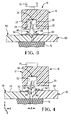
- FIGURE 3 is a cross-sectional view of the connector of Figure 2 mounted to two adjacent co-planar circuit-bearing substrates.
- FIGURE 4 is a view similar to that of Figure 3 wherein the substrates are spaced from each other in both in a horizontal as well as a vertical direction.
- FIGURE 5 is plan view of a contact made in accordance with the invention.
- connector 10 for interconnecting circuits of adjacent circuit-bearing substrates 50, 60 having circuit termini 52, 62 adjacent edges thereof includes a housing 12 having at least one contact-receiving cavity 20 and a contact 30 disposed therein.
- the contact-receiving cavity 20 includes a top wall 22 and opposed side walls 24 and is open to the mounting face 14 of housing 12, as seen in Figure 3.
- connector 10 is shown being used in an electrical article 64 that is mountable to a base 70 of an electronic apparatus.
- Housing 12 further includes mounting portions 16 having apertures 18 extending therethrough for receiving fastening devices 74 for securing connector 10 to electrical article 64 and to base 70.
- Each fastening device 74 extends through a respective washer 75, an insert 76 disposed in housing aperture 18, a respective aperture 66 in article 64 and are secured in a threaded aperture 72 of base 70.
- Insert 76 has a diameter dimensioned to be received in aperture 18 in an interference fit and a length selected to be at least equal to the depth of aperture 18, thereby preventing the housing 12 from being damaged when the fastening device 74 is secured to base 72.
- insert 76 provides a stop surface for fastening device 74.
- the length of fastening device 74 and insert 76 are selected to apply the desired amount of compression force against housing 12 and the contacts 30 therein to assure electrical connection between the circuit termini 52, 62. It is to be understood that other types of fastening devices may also be used.
- Contact 30 as best seen in Figure 5, includes a plate-like body section 32 having two pairs of opposed edges 34, 36,respectively, and a pair of elongate spring arm contact sections 40 co-extending from a common edge 34 of the body section 32 and outwardly from the contact-receiving cavity 20 when the contact 30 is secured in housing 12.
- Each contact 30 is secured in a respective cavity in an interference fit whereby the edges 36 include a plurality of protrusions 37 that engage the inner surfaces of side walls 24 of cavity 20.
- the elongate spring arm contact sections 40 have end portions 42 arcuately diverging from each other, all within the plane of the body section to free ends 44 to orient respective continuous arcuate edges 46 thereof to face away from the mounting face 14.
- the arcuate edges 46 are adapted to be engaged by associated circuit termini 52, 62 of respective ones of the circuit-bearing substrates 50, 60.
- the elongate spring arm contact sections 40 are independently deflectable toward the mounting face 14 of housing 12 under spring bias, upon engagement with circuit termini 52, 62 when compressed there against,such that the circuit-bearing substrates 50, 60 can vary relatively in distance from the mounting face 14, (Y axis) and from each other (X axis), as shown representatively in Figure 4.
- the corresponding termini 52, 62 are aligned in the one direction (Z axis).
- Figures 3 and 4 illustrate the cross-sectional view of the connector 10 mounted to circuit board wherein the adjacent substrates 50, 60 lie in a common plane in Figure 3, and in Figure 4,they are separated vertically by a distance ⁇ and horizontally by a distance ⁇ .
- the circuit-bearing substrates or circuit boards 50, 60 are aligned such that the corresponding circuit termini 52, 62 are in alignment with each other with respect to the Z direction in the apparatus, spaced apart or adjacent in the X direction and co-planar or vertically spaced in the Y direction,as shown in Figure 4.
- the housing is made from a dielectric material, such as a liquid crystal polymer or other material, as known in the art, that is suitable for use in the desired type of environment.
- the terminals are stamped from a strip of metal, such as beryllium copper, phosphor bronze or the like.
- the mounting portions 16 of housing 12 are secured to base 70.
- the base 70 extends beneath the co-planar circuit-bearing substrates 50, 60.
- Substrates 50 and 60 are of the same thickness, such that the corresponding upper and lower surfaces lie on respective common planes.
- the circuit-bearing substrates 50, 60 are of different thicknesses resulting in vertical difference ⁇ . The lower surfaces of the substrates lie on the same plane, but the upper surfaces are on different planes.
- the connector of the present invention provides a contact having resilient legs that can adjust to differences in height (step) and spacing (gap) between aligned circuit termini on adjacent circuit-bearing substrates.
- the resilient spring arms provide sufficient normal force to retain the connection for each individual trace independently and compensate for variances in a gap or step between the two boards.
- the spring arms maintain their resiliency when subject to changes in temperature and when used in an apparatus that is subject to periodic or continual vibrations.
- the connector of the present invention can be removed from a first location having a first gap and step arrangement and used in a second location having a second gap and step arrangement.
Landscapes
- Coupling Device And Connection With Printed Circuit (AREA)
Applications Claiming Priority (2)
| Application Number | Priority Date | Filing Date | Title |
|---|---|---|---|
| US5929297P | 1997-09-18 | 1997-09-18 | |
| US59292P | 1997-09-18 |
Publications (2)
| Publication Number | Publication Date |
|---|---|
| EP0903810A2 true EP0903810A2 (de) | 1999-03-24 |
| EP0903810A3 EP0903810A3 (de) | 2000-03-29 |
Family
ID=22022050
Family Applications (1)
| Application Number | Title | Priority Date | Filing Date |
|---|---|---|---|
| EP98307287A Withdrawn EP0903810A3 (de) | 1997-09-18 | 1998-09-09 | Verbinder für aneinander grenzende schaltungstragende Substraten |
Country Status (2)
| Country | Link |
|---|---|
| EP (1) | EP0903810A3 (de) |
| JP (1) | JPH11144825A (de) |
Cited By (2)
| Publication number | Priority date | Publication date | Assignee | Title |
|---|---|---|---|---|
| FR2806536A1 (fr) * | 2000-03-20 | 2001-09-21 | Raymond Bernier | Dispositif d'interconnexion electrique de deux composants a plages de contact |
| DE102011103854A1 (de) * | 2011-05-25 | 2012-11-29 | Lumberg Connect Gmbh | Verbinder zur Konnektierung zweier Leiterplatten |
Families Citing this family (2)
| Publication number | Priority date | Publication date | Assignee | Title |
|---|---|---|---|---|
| JP5717472B2 (ja) * | 2011-03-07 | 2015-05-13 | 富士通コンポーネント株式会社 | コネクタ |
| JP2013030434A (ja) * | 2011-07-29 | 2013-02-07 | Yamaichi Electronics Co Ltd | 電気コネクタ |
Family Cites Families (7)
| Publication number | Priority date | Publication date | Assignee | Title |
|---|---|---|---|---|
| GB1359671A (en) * | 1972-04-25 | 1974-07-10 | Ferranti Ltd | Connectors for printed circuit boards |
| JPS5555985U (de) * | 1978-10-12 | 1980-04-16 | ||
| FR2627639A1 (fr) * | 1988-02-19 | 1989-08-25 | Thomson Csf | Dispositif de fixation de connexions notamment applicable a la connectique haute densite |
| GB2273830B (en) * | 1992-12-24 | 1997-04-16 | Whitaker Corp | Electrical contact elements for interposer structures |
| US5336095A (en) * | 1993-05-13 | 1994-08-09 | The Whitaker Corporation | Flex circuit interface for co-planar PCBs |
| NL9301779A (nl) * | 1993-10-14 | 1995-05-01 | Connector Systems Tech Nv | Elektrische connector voor montage op het oppervlak van een printplaat. |
| DE19617121C1 (de) * | 1996-04-29 | 1997-07-24 | Lumberg Karl Gmbh & Co | Kontaktleiste für Leiterplatten |
-
1998
- 1998-09-09 EP EP98307287A patent/EP0903810A3/de not_active Withdrawn
- 1998-09-10 JP JP10256559A patent/JPH11144825A/ja active Pending
Cited By (3)
| Publication number | Priority date | Publication date | Assignee | Title |
|---|---|---|---|---|
| FR2806536A1 (fr) * | 2000-03-20 | 2001-09-21 | Raymond Bernier | Dispositif d'interconnexion electrique de deux composants a plages de contact |
| DE102011103854A1 (de) * | 2011-05-25 | 2012-11-29 | Lumberg Connect Gmbh | Verbinder zur Konnektierung zweier Leiterplatten |
| DE102011103854B4 (de) * | 2011-05-25 | 2015-04-02 | Lumberg Connect Gmbh | Verbinder zur Konnektierung zweier Leiterplatten |
Also Published As
| Publication number | Publication date |
|---|---|
| EP0903810A3 (de) | 2000-03-29 |
| JPH11144825A (ja) | 1999-05-28 |
Similar Documents
| Publication | Publication Date | Title |
|---|---|---|
| US6109927A (en) | Connector for adjacent circuit-bearing substrates | |
| US5427535A (en) | Resilient electrically conductive terminal assemblies | |
| US4144648A (en) | Connector | |
| US5073119A (en) | Surface mount electrical connector | |
| US4645279A (en) | Chip carrier socket having improved contact terminals | |
| EP0374460B1 (de) | Elektrischer Verbinder unter Verwendung einer Leiterplatte | |
| US5336094A (en) | Apparatus for interconnecting electrical contacts | |
| US6249440B1 (en) | Contact arrangement for detachably attaching an electric component, especially an integrated circuit to a printed circuit board | |
| KR100776894B1 (ko) | 간단한 구조를 가지며 안정된 접속이 가능한 전기접속 부재및 그것을 사용하는 커넥터 | |
| US11196207B2 (en) | Card edge connector with protective cover | |
| US4894022A (en) | Solderless surface mount card edge connector | |
| US6358063B1 (en) | Sealed interposer assembly | |
| KR100526008B1 (ko) | Pga용 콘택트 및 pga 소켓 | |
| CA2680734A1 (en) | Edge-to-edge connector system for electronic devices | |
| US6835071B2 (en) | Elastomeric connector interconnecting flexible circuits and circuit board and method of manufacturing the same | |
| KR970054942A (ko) | 표면 장착식 저 프로파일 전기 커넥터 조립체 | |
| KR100341845B1 (ko) | 기판용컨넥터 | |
| US5691509A (en) | Flexible cable termination and connector system | |
| WO1997008779A1 (en) | Right angle electrical connector | |
| EP0903810A2 (de) | Verbinder für aneinander grenzende schaltungstragende Substraten | |
| KR100228457B1 (ko) | 접속 장치 | |
| CN1319218C (zh) | 具有用于接地的连接板的电连接器 | |
| JP4240499B2 (ja) | 接続部材 | |
| EP0829188B1 (de) | Kontaktanordnung zum lösbaren befestigen eines elektrischen bauteiles,insbesondere eines integrierten schaltkreises auf einer leiterplatte | |
| FI89842C (fi) | Fjaedrande kontaktdon foer radiofrekventa signaler |
Legal Events
| Date | Code | Title | Description |
|---|---|---|---|
| PUAI | Public reference made under article 153(3) epc to a published international application that has entered the european phase |
Free format text: ORIGINAL CODE: 0009012 |
|
| AK | Designated contracting states |
Kind code of ref document: A2 Designated state(s): DE FR GB |
|
| AX | Request for extension of the european patent |
Free format text: AL;LT;LV;MK;RO;SI |
|
| PUAL | Search report despatched |
Free format text: ORIGINAL CODE: 0009013 |
|
| AK | Designated contracting states |
Kind code of ref document: A3 Designated state(s): AT BE CH CY DE DK ES FI FR GB GR IE IT LI LU MC NL PT SE |
|
| AX | Request for extension of the european patent |
Free format text: AL;LT;LV;MK;RO;SI |
|
| 17P | Request for examination filed |
Effective date: 20000928 |
|
| AKX | Designation fees paid |
Free format text: DE FR GB |
|
| GRAP | Despatch of communication of intention to grant a patent |
Free format text: ORIGINAL CODE: EPIDOSNIGR1 |
|
| RIC1 | Information provided on ipc code assigned before grant |
Ipc: 7H 01R 12/04 A |
|
| STAA | Information on the status of an ep patent application or granted ep patent |
Free format text: STATUS: THE APPLICATION IS DEEMED TO BE WITHDRAWN |
|
| 18D | Application deemed to be withdrawn |
Effective date: 20031211 |