EP0903787A2 - Dispositif de réduction du bruit dans un transistor à hyperfréquences et méthode pour sa fabrication - Google Patents
Dispositif de réduction du bruit dans un transistor à hyperfréquences et méthode pour sa fabrication Download PDFInfo
- Publication number
- EP0903787A2 EP0903787A2 EP98116217A EP98116217A EP0903787A2 EP 0903787 A2 EP0903787 A2 EP 0903787A2 EP 98116217 A EP98116217 A EP 98116217A EP 98116217 A EP98116217 A EP 98116217A EP 0903787 A2 EP0903787 A2 EP 0903787A2
- Authority
- EP
- European Patent Office
- Prior art keywords
- buried layer
- layer
- contact
- transistor
- pad
- Prior art date
- Legal status (The legal status is an assumption and is not a legal conclusion. Google has not performed a legal analysis and makes no representation as to the accuracy of the status listed.)
- Withdrawn
Links
- 238000000034 method Methods 0.000 title claims abstract description 5
- 238000004519 manufacturing process Methods 0.000 title claims description 5
- 239000000758 substrate Substances 0.000 claims description 18
- 239000010410 layer Substances 0.000 description 32
- 230000003071 parasitic effect Effects 0.000 description 9
- 238000010586 diagram Methods 0.000 description 2
- 238000009413 insulation Methods 0.000 description 2
- 101001042415 Cratylia mollis Mannose/glucose-specific lectin Cramoll Proteins 0.000 description 1
- 102100038742 Cytochrome P450 2A13 Human genes 0.000 description 1
- 102100029775 Eukaryotic translation initiation factor 1 Human genes 0.000 description 1
- LFERELMXERXKKQ-KMXXXSRASA-N Fenugreekine Chemical compound NC(=O)C1=CC=CC([C@H]2[C@@H]([C@H](O)[C@@H](COP(O)(=O)OP(O)(=O)OC[C@@H]3[C@H]([C@@H](O)[C@@H](O3)N3C4=NC=NC(N)=C4N=C3)O)O2)O)=N1 LFERELMXERXKKQ-KMXXXSRASA-N 0.000 description 1
- 101000957389 Homo sapiens Cytochrome P450 2A13 Proteins 0.000 description 1
- 101001012787 Homo sapiens Eukaryotic translation initiation factor 1 Proteins 0.000 description 1
- 101000643378 Homo sapiens Serine racemase Proteins 0.000 description 1
- XUIMIQQOPSSXEZ-UHFFFAOYSA-N Silicon Chemical compound [Si] XUIMIQQOPSSXEZ-UHFFFAOYSA-N 0.000 description 1
- 239000003990 capacitor Substances 0.000 description 1
- AIXMJTYHQHQJLU-UHFFFAOYSA-N chembl210858 Chemical compound O1C(CC(=O)OC)CC(C=2C=CC(O)=CC=2)=N1 AIXMJTYHQHQJLU-UHFFFAOYSA-N 0.000 description 1
- 238000011161 development Methods 0.000 description 1
- 230000018109 developmental process Effects 0.000 description 1
- 238000002513 implantation Methods 0.000 description 1
- 239000002184 metal Substances 0.000 description 1
- 229910052710 silicon Inorganic materials 0.000 description 1
- 239000010703 silicon Substances 0.000 description 1
- 239000002344 surface layer Substances 0.000 description 1
Images
Classifications
-
- H—ELECTRICITY
- H10—SEMICONDUCTOR DEVICES; ELECTRIC SOLID-STATE DEVICES NOT OTHERWISE PROVIDED FOR
- H10D—INORGANIC ELECTRIC SEMICONDUCTOR DEVICES
- H10D10/00—Bipolar junction transistors [BJT]
- H10D10/40—Vertical BJTs
-
- H—ELECTRICITY
- H10—SEMICONDUCTOR DEVICES; ELECTRIC SOLID-STATE DEVICES NOT OTHERWISE PROVIDED FOR
- H10D—INORGANIC ELECTRIC SEMICONDUCTOR DEVICES
- H10D62/00—Semiconductor bodies, or regions thereof, of devices having potential barriers
- H10D62/10—Shapes, relative sizes or dispositions of the regions of the semiconductor bodies; Shapes of the semiconductor bodies
- H10D62/13—Semiconductor regions connected to electrodes carrying current to be rectified, amplified or switched, e.g. source or drain regions
- H10D62/137—Collector regions of BJTs
Definitions
- the invention relates to minimizing the noise figure Microwave transistors.
- This noise figure is like the name already says a measure of a component's noise and with ever smaller dimensions of the components and always higher operating frequencies increasingly due to the influence the parasitic elements on the chip, for example lines, Contact areas and the substrate resistance.
- the object on which the invention is based is now an arrangement for reducing noise in microwave transistors to indicate at which the reduction of the Noise figure of the transistor in the simplest possible way and if possible without changing the usual manufacturing processes for Microwave transistors in silicon bipolar technology is feasible.
- This task is regarding the arrangement by the features of claim 1 and in terms the manufacturing process by the features of the claim 5 solved.
- the claims 2 to 4 relate to advantageous Developments of the arrangement according to the invention.
- the noise figure is reduced in a simple manner in that a low-resistance buried one under the base connection surface Layer is introduced into the substrate, which is close to the Basic connection via a standard collector contact with reference potential connected is. Because the noise figure of the entire Arrangement not only of the actual active component, but also from the dimensioning of the elements of a parasitic RC elements between the base connection and reference potential depends on the noise figure of the arrangement due to a low-resistance ground connection of the capacitor of the parasitic RC links lowered.
- a buried one Layer if necessary, by deep implantation generated layer and also the metallic connection of this Layers with ground potential in the same process as that Layers between the collector and the collector connection and the layer for the collector connection itself is formed become.
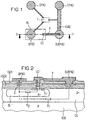
- FIG. 1 is an arrangement with a microwave transistor T shown with a collector pad CPAD, a base pad BPAD and an emitter pad EPAD is connected, wherein the emitter pad with a SUBPAD substrate connection area for contacting a Substrate and connected to ground (GRD).
- GRD ground
- a buried layer BL ' In the lateral Area of the base pad and towards SUBPAD extended substrate pad is a lateral boundary line a buried layer BL 'in the form of a Rectangle indicated.
- a buried layer BL ' In the lateral Area of the base pad and towards SUBPAD extended substrate pad is a lateral boundary line a buried layer BL 'in the form of a Rectangle indicated.
- Between the SUBPAD substrate connection and the lateral region of the buried layer BL ' is one web-like metal connection V shown up inside of the lateral region of the buried layer is sufficient and has a contact CC '.
- Section line 2-2 through
- FIG 2 the section along the line 2-2 'is shown, in which between the base pad EPAD and the buried layer BL', which from the base pad z. B. is separated by insulation layers ISO1 and ISO2, a parasitic capacitance C is located.
- the buried layer BL ' is connected to the contact CC' either directly or via an additional deeply implanted layer TI '.
- the connection of the parasitic capacitance C located in the buried layer BL ' is connected via a parasitic resistor R2 to the contact CC', which represents the buried layer BL or the deeply implanted layer TI '.
- connection of the parasitic capacitance C located in the buried layer BL' would be connected to the substrate connection surface SUBPAD via a substantially higher-resistance parasitic resistor R 1 , which is shown in broken lines.
- the sheet resistance of the buried layer BL ' is typically at approx. 20 to 40 ⁇ / ⁇ and is therefore typical 0.1 times lower than the sheet resistance of the substrate. Provided an additional one covers the entire buried layer extending deeply implanted layer TI is present, the resistance can be reduced again can be achieved by a factor of 0.5.
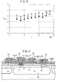
- a so-called channel stop layer CS which is more heavily doped than the substrate, is often located between the insulation layer ISO2 and the substrate SUB.
- the layer BL ' is typically doped by a factor of 100 higher than the layer CS and is n-conductive here, whereas the channel stop layer CS and the substrate are p-conductive. Because of the significantly higher doping of the buried layer and the greater proximity to the ground potential, the resistance R 2 is also significantly lower than the resistance of a conventional arrangement with a channel stop layer.
- FIG. 3 shows the influence of the substrate resistance on the minimum noise figure on the basis of some measured values plotted against the frequency f, the minimum possible noise figure being determined in each case by reducing the noise figure of an arrangement with transistor T by the noise figure of an empty arrangement without transistor T. It is clear from this that the minimum noise figure F min can be reduced by approximately 0.5 at frequencies of approximately 3 GHz and with increasing frequency up to approximately 0.8 at a frequency of 7 GHz.
- Figure 4 is a section through a conventional microwave transistor with the contacting of a collector C via a buried layer BL and a deeply implanted layer TI shown with the collector contact CC. From Figure 4 together with Figure 2 it is clear that the buried layer BL ', the deeply implanted layer TI' and the contact CC 'save costs at the same time in the standard process for contacting of the collector can be generated, the commonly generated items in their reference numerals only distinguish by a line.
Landscapes
- Bipolar Transistors (AREA)
- Bipolar Integrated Circuits (AREA)
- Semiconductor Integrated Circuits (AREA)
- Transforming Light Signals Into Electric Signals (AREA)
Applications Claiming Priority (2)
| Application Number | Priority Date | Filing Date | Title |
|---|---|---|---|
| DE19740909A DE19740909C2 (de) | 1997-09-17 | 1997-09-17 | Anordnung zur Reduktion von Rauschen bei Mikrowellentransistoren und Verfahren zu deren Herstellung |
| DE19740909 | 1997-09-17 |
Publications (2)
| Publication Number | Publication Date |
|---|---|
| EP0903787A2 true EP0903787A2 (fr) | 1999-03-24 |
| EP0903787A3 EP0903787A3 (fr) | 1999-12-08 |
Family
ID=7842660
Family Applications (1)
| Application Number | Title | Priority Date | Filing Date |
|---|---|---|---|
| EP98116217A Withdrawn EP0903787A3 (fr) | 1997-09-17 | 1998-08-27 | Dispositif de réduction du bruit dans un transistor à hyperfréquences et méthode pour sa fabrication |
Country Status (4)
| Country | Link |
|---|---|
| US (1) | US6069404A (fr) |
| EP (1) | EP0903787A3 (fr) |
| JP (1) | JP3973777B2 (fr) |
| DE (1) | DE19740909C2 (fr) |
Families Citing this family (5)
| Publication number | Priority date | Publication date | Assignee | Title |
|---|---|---|---|---|
| US6612852B1 (en) | 2000-04-13 | 2003-09-02 | Molex Incorporated | Contactless interconnection system |
| US6362972B1 (en) | 2000-04-13 | 2002-03-26 | Molex Incorporated | Contactless interconnection system |
| US6837719B2 (en) * | 2002-02-25 | 2005-01-04 | Molex Incorporated | Connector with included filtered power delivery |
| JP4626935B2 (ja) * | 2002-10-01 | 2011-02-09 | ルネサスエレクトロニクス株式会社 | 半導体装置及びその製造方法 |
| US6946720B2 (en) * | 2003-02-13 | 2005-09-20 | Intersil Americas Inc. | Bipolar transistor for an integrated circuit having variable value emitter ballast resistors |
Family Cites Families (2)
| Publication number | Priority date | Publication date | Assignee | Title |
|---|---|---|---|---|
| JPH07109831B2 (ja) * | 1990-01-25 | 1995-11-22 | 株式会社東芝 | 半導体装置 |
| EP0632505B1 (fr) * | 1993-07-01 | 1997-10-01 | Co.Ri.M.Me. Consorzio Per La Ricerca Sulla Microelettronica Nel Mezzogiorno | Transistor bipolaire vertical à puissance avec une base enterrée et une géométrie interdigitée |
-
1997
- 1997-09-17 DE DE19740909A patent/DE19740909C2/de not_active Expired - Fee Related
-
1998
- 1998-08-27 EP EP98116217A patent/EP0903787A3/fr not_active Withdrawn
- 1998-09-16 JP JP26159998A patent/JP3973777B2/ja not_active Expired - Fee Related
- 1998-09-17 US US09/156,202 patent/US6069404A/en not_active Expired - Lifetime
Also Published As
| Publication number | Publication date |
|---|---|
| DE19740909C2 (de) | 1999-07-01 |
| DE19740909A1 (de) | 1999-03-25 |
| JP3973777B2 (ja) | 2007-09-12 |
| JPH11145152A (ja) | 1999-05-28 |
| EP0903787A3 (fr) | 1999-12-08 |
| US6069404A (en) | 2000-05-30 |
Similar Documents
| Publication | Publication Date | Title |
|---|---|---|
| DE3586268T2 (de) | Eingangs-schutzanordnung fuer vlsi-schaltungsanordnungen. | |
| DE1614373C2 (fr) | ||
| EP1556899B1 (fr) | Composant electronique a composant electronique passif integre et procede de fabrication dudit composant | |
| DE3714672A1 (de) | Rc-leitung | |
| DE69232199T2 (de) | Halbleiteranordnung mit verbessertem Frequenzgang | |
| DE1764712A1 (de) | Widerstandskoerper fuer eine integrierte Schaltung | |
| EP0903787A2 (fr) | Dispositif de réduction du bruit dans un transistor à hyperfréquences et méthode pour sa fabrication | |
| DE3119288A1 (de) | Halbleiteranordnung | |
| DE69026675T2 (de) | MIS-Kapazitätselement | |
| DE2406807A1 (de) | Integrierte halbleiterschaltung | |
| US7642188B2 (en) | Mixed signal integrated circuit with improved isolation | |
| DE102011083038B4 (de) | Transistor und Verfahren zum Herstellen eines Transistors und zum Herstellen eines Halbleiterbauelements | |
| DE3786693T2 (de) | Programmierbarer Kontaktfleck. | |
| DE69706721T2 (de) | Zener-Zap-Diode und Verfahren zur Herstellung | |
| DE3103785A1 (de) | Halbleiteranordnung mit hoher durchbruchspannung | |
| DE2544907C2 (fr) | ||
| DE3887873T2 (de) | Phantom-esd-schutzschaltung mit e-feldverdichtung. | |
| DE10341564B4 (de) | Kondensatoranordnung und Verfahren zur Herstellung derselben | |
| DE60131650T2 (de) | Kondensator mit veränderlicher Kapazität | |
| DE2046053B2 (de) | Integrierte Schaltung | |
| EP0562354A2 (fr) | Dispositif de circuit intégré | |
| DE3740302C2 (fr) | ||
| DE19825608C1 (de) | Integrierte Halbleiterschaltung mit einer Anschlußfläche, die eine fein abgestufte RC-Charakteristik aufweist | |
| DE10041691A1 (de) | Halbleiteranordnung | |
| DE19818024A1 (de) | Halbleitervorrichtung mit einer Trennstruktur für eine hohe Haltespannung |
Legal Events
| Date | Code | Title | Description |
|---|---|---|---|
| PUAI | Public reference made under article 153(3) epc to a published international application that has entered the european phase |
Free format text: ORIGINAL CODE: 0009012 |
|
| AK | Designated contracting states |
Kind code of ref document: A2 Designated state(s): DE FR GB |
|
| AX | Request for extension of the european patent |
Free format text: AL;LT;LV;MK;RO;SI |
|
| PUAL | Search report despatched |
Free format text: ORIGINAL CODE: 0009013 |
|
| AK | Designated contracting states |
Kind code of ref document: A3 Designated state(s): AT BE CH CY DE DK ES FI FR GB GR IE IT LI LU MC NL PT SE |
|
| AX | Request for extension of the european patent |
Free format text: AL;LT;LV;MK;RO;SI |
|
| 17P | Request for examination filed |
Effective date: 20000105 |
|
| AKX | Designation fees paid |
Free format text: DE FR GB |
|
| RAP1 | Party data changed (applicant data changed or rights of an application transferred) |
Owner name: INFINEON TECHNOLOGIES AG |
|
| STAA | Information on the status of an ep patent application or granted ep patent |
Free format text: STATUS: THE APPLICATION HAS BEEN WITHDRAWN |
|
| 18W | Application withdrawn |
Effective date: 20040414 |