EP0903787A2 - Device for reducing noise in microwave transistors and method for its fabrication - Google Patents
Device for reducing noise in microwave transistors and method for its fabrication Download PDFInfo
- Publication number
- EP0903787A2 EP0903787A2 EP98116217A EP98116217A EP0903787A2 EP 0903787 A2 EP0903787 A2 EP 0903787A2 EP 98116217 A EP98116217 A EP 98116217A EP 98116217 A EP98116217 A EP 98116217A EP 0903787 A2 EP0903787 A2 EP 0903787A2
- Authority
- EP
- European Patent Office
- Prior art keywords
- buried layer
- layer
- contact
- transistor
- pad
- Prior art date
- Legal status (The legal status is an assumption and is not a legal conclusion. Google has not performed a legal analysis and makes no representation as to the accuracy of the status listed.)
- Withdrawn
Links
- 238000000034 method Methods 0.000 title claims abstract description 5
- 238000004519 manufacturing process Methods 0.000 title claims description 5
- 239000000758 substrate Substances 0.000 claims description 18
- 239000010410 layer Substances 0.000 description 32
- 230000003071 parasitic effect Effects 0.000 description 9
- 238000010586 diagram Methods 0.000 description 2
- 238000009413 insulation Methods 0.000 description 2
- 101001042415 Cratylia mollis Mannose/glucose-specific lectin Cramoll Proteins 0.000 description 1
- 102100038742 Cytochrome P450 2A13 Human genes 0.000 description 1
- 102100029775 Eukaryotic translation initiation factor 1 Human genes 0.000 description 1
- LFERELMXERXKKQ-KMXXXSRASA-N Fenugreekine Chemical compound NC(=O)C1=CC=CC([C@H]2[C@@H]([C@H](O)[C@@H](COP(O)(=O)OP(O)(=O)OC[C@@H]3[C@H]([C@@H](O)[C@@H](O3)N3C4=NC=NC(N)=C4N=C3)O)O2)O)=N1 LFERELMXERXKKQ-KMXXXSRASA-N 0.000 description 1
- 101000957389 Homo sapiens Cytochrome P450 2A13 Proteins 0.000 description 1
- 101001012787 Homo sapiens Eukaryotic translation initiation factor 1 Proteins 0.000 description 1
- 101000643378 Homo sapiens Serine racemase Proteins 0.000 description 1
- XUIMIQQOPSSXEZ-UHFFFAOYSA-N Silicon Chemical compound [Si] XUIMIQQOPSSXEZ-UHFFFAOYSA-N 0.000 description 1
- 239000003990 capacitor Substances 0.000 description 1
- AIXMJTYHQHQJLU-UHFFFAOYSA-N chembl210858 Chemical compound O1C(CC(=O)OC)CC(C=2C=CC(O)=CC=2)=N1 AIXMJTYHQHQJLU-UHFFFAOYSA-N 0.000 description 1
- 238000011161 development Methods 0.000 description 1
- 230000018109 developmental process Effects 0.000 description 1
- 238000002513 implantation Methods 0.000 description 1
- 239000002184 metal Substances 0.000 description 1
- 229910052710 silicon Inorganic materials 0.000 description 1
- 239000010703 silicon Substances 0.000 description 1
- 239000002344 surface layer Substances 0.000 description 1
Images
Classifications
-
- H—ELECTRICITY
- H10—SEMICONDUCTOR DEVICES; ELECTRIC SOLID-STATE DEVICES NOT OTHERWISE PROVIDED FOR
- H10D—INORGANIC ELECTRIC SEMICONDUCTOR DEVICES
- H10D10/00—Bipolar junction transistors [BJT]
- H10D10/40—Vertical BJTs
-
- H—ELECTRICITY
- H10—SEMICONDUCTOR DEVICES; ELECTRIC SOLID-STATE DEVICES NOT OTHERWISE PROVIDED FOR
- H10D—INORGANIC ELECTRIC SEMICONDUCTOR DEVICES
- H10D62/00—Semiconductor bodies, or regions thereof, of devices having potential barriers
- H10D62/10—Shapes, relative sizes or dispositions of the regions of the semiconductor bodies; Shapes of the semiconductor bodies
- H10D62/13—Semiconductor regions connected to electrodes carrying current to be rectified, amplified or switched, e.g. source or drain regions
- H10D62/137—Collector regions of BJTs
Definitions
- the invention relates to minimizing the noise figure Microwave transistors.
- This noise figure is like the name already says a measure of a component's noise and with ever smaller dimensions of the components and always higher operating frequencies increasingly due to the influence the parasitic elements on the chip, for example lines, Contact areas and the substrate resistance.
- the object on which the invention is based is now an arrangement for reducing noise in microwave transistors to indicate at which the reduction of the Noise figure of the transistor in the simplest possible way and if possible without changing the usual manufacturing processes for Microwave transistors in silicon bipolar technology is feasible.
- This task is regarding the arrangement by the features of claim 1 and in terms the manufacturing process by the features of the claim 5 solved.
- the claims 2 to 4 relate to advantageous Developments of the arrangement according to the invention.
- the noise figure is reduced in a simple manner in that a low-resistance buried one under the base connection surface Layer is introduced into the substrate, which is close to the Basic connection via a standard collector contact with reference potential connected is. Because the noise figure of the entire Arrangement not only of the actual active component, but also from the dimensioning of the elements of a parasitic RC elements between the base connection and reference potential depends on the noise figure of the arrangement due to a low-resistance ground connection of the capacitor of the parasitic RC links lowered.
- a buried one Layer if necessary, by deep implantation generated layer and also the metallic connection of this Layers with ground potential in the same process as that Layers between the collector and the collector connection and the layer for the collector connection itself is formed become.
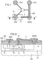
- FIG. 1 is an arrangement with a microwave transistor T shown with a collector pad CPAD, a base pad BPAD and an emitter pad EPAD is connected, wherein the emitter pad with a SUBPAD substrate connection area for contacting a Substrate and connected to ground (GRD).
- GRD ground
- a buried layer BL ' In the lateral Area of the base pad and towards SUBPAD extended substrate pad is a lateral boundary line a buried layer BL 'in the form of a Rectangle indicated.
- a buried layer BL ' In the lateral Area of the base pad and towards SUBPAD extended substrate pad is a lateral boundary line a buried layer BL 'in the form of a Rectangle indicated.
- Between the SUBPAD substrate connection and the lateral region of the buried layer BL ' is one web-like metal connection V shown up inside of the lateral region of the buried layer is sufficient and has a contact CC '.
- Section line 2-2 through
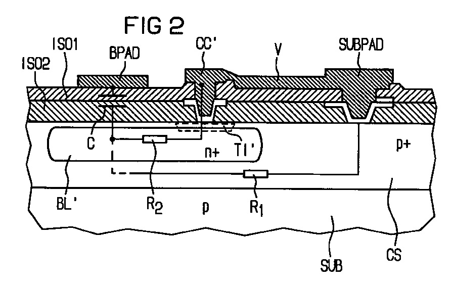
- FIG 2 the section along the line 2-2 'is shown, in which between the base pad EPAD and the buried layer BL', which from the base pad z. B. is separated by insulation layers ISO1 and ISO2, a parasitic capacitance C is located.
- the buried layer BL ' is connected to the contact CC' either directly or via an additional deeply implanted layer TI '.
- the connection of the parasitic capacitance C located in the buried layer BL ' is connected via a parasitic resistor R2 to the contact CC', which represents the buried layer BL or the deeply implanted layer TI '.
- connection of the parasitic capacitance C located in the buried layer BL' would be connected to the substrate connection surface SUBPAD via a substantially higher-resistance parasitic resistor R 1 , which is shown in broken lines.
- the sheet resistance of the buried layer BL ' is typically at approx. 20 to 40 ⁇ / ⁇ and is therefore typical 0.1 times lower than the sheet resistance of the substrate. Provided an additional one covers the entire buried layer extending deeply implanted layer TI is present, the resistance can be reduced again can be achieved by a factor of 0.5.
- a so-called channel stop layer CS which is more heavily doped than the substrate, is often located between the insulation layer ISO2 and the substrate SUB.
- the layer BL ' is typically doped by a factor of 100 higher than the layer CS and is n-conductive here, whereas the channel stop layer CS and the substrate are p-conductive. Because of the significantly higher doping of the buried layer and the greater proximity to the ground potential, the resistance R 2 is also significantly lower than the resistance of a conventional arrangement with a channel stop layer.
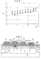
- FIG. 3 shows the influence of the substrate resistance on the minimum noise figure on the basis of some measured values plotted against the frequency f, the minimum possible noise figure being determined in each case by reducing the noise figure of an arrangement with transistor T by the noise figure of an empty arrangement without transistor T. It is clear from this that the minimum noise figure F min can be reduced by approximately 0.5 at frequencies of approximately 3 GHz and with increasing frequency up to approximately 0.8 at a frequency of 7 GHz.
- Figure 4 is a section through a conventional microwave transistor with the contacting of a collector C via a buried layer BL and a deeply implanted layer TI shown with the collector contact CC. From Figure 4 together with Figure 2 it is clear that the buried layer BL ', the deeply implanted layer TI' and the contact CC 'save costs at the same time in the standard process for contacting of the collector can be generated, the commonly generated items in their reference numerals only distinguish by a line.
Landscapes
- Bipolar Transistors (AREA)
- Bipolar Integrated Circuits (AREA)
- Transforming Light Signals Into Electric Signals (AREA)
- Semiconductor Integrated Circuits (AREA)
Abstract
Der Anmeldungsgegenstand betrifft eine Anordnung, bei der die
minimale Rauschzahl dadurch reduziert wird, daß unterhalb der
Basisanschlußfläche eine hoch dotierte vergrabene Schicht
(BL') hergestellt wird, die in der Nähe der Basisanschlußfläche
über einen Standard-Kollektorkontakt (CC') mit Bezugspotential
(GRD) verbunden ist. Vorteilhaft ist hierbei die Senkung
der minimalen Rauschzahl ohne zusätzliche Prozeßschritte.
Description
Die Erfindung betrifft die Minimierung der Rauschzahl bei Mikrowellentransistoren. Diese Rauschzahl ist, wie der Name bereits sagt, ein Maß für das Rauschen eines Bauelements und wird mit immer kleineren Abmessungen der Bauelemente und immer höheren Betriebsfrequenzen zunehmend durch den Einfluß der parasitären Elemente am Chip, zum Beispiel Leitungen, Kontaktflächen und dem Substratwiderstand, beeinflußt.The invention relates to minimizing the noise figure Microwave transistors. This noise figure is like the name already says a measure of a component's noise and with ever smaller dimensions of the components and always higher operating frequencies increasingly due to the influence the parasitic elements on the chip, for example lines, Contact areas and the substrate resistance.
Aus dem IEEE Paper zum Microwave and Millimeter-Wave Monolithic Circuits Symposium, 1994, pp. 225 bis 228, ist beispielsweise eine Modellierung mit Ersatzschaltbildern bekannt, die zeigt, daß beispielsweise die parasitären Effekte aufgrund der Anschlußpads mit steigender Frequenz einen starken Einfluß auf die Rauschzahl haben.From the IEEE paper on Microwave and Millimeter-Wave Monolithic Circuits Symposium, 1994, pp. 225 to 228, for example modeling with equivalent circuit diagrams known, which shows that, for example, the parasitic effects strong due to the connection pads with increasing frequency Have an influence on the noise figure.
Die der Erfindung zugrundeliegende Aufgabe liegt nun darin,
eine Anordnung zur Reduktion von Rauschen bei Mikrowellentransistoren
anzugeben, bei der die Verkleinerung der
Rauschzahl des Transistors auf möglichst einfache Weise und
möglichst ohne Änderung üblicher Herstellungsprozesse für
Mikrowellentransistoren in Silizium-Bipolar-Technologie
durchführbar ist. Diese Aufgabe wird hinsichtlich der Anordnung
durch die Merkmale des Patentanspruchs 1 und hinsichtlich
des Herstellverfahrens durch die Merkmale des Anspruchs
5 gelöst. Die Patentansprüche 2 bis 4 betreffen vorteilhafte
Weiterbildungen der erfindungsgemäßen Anordnung.The object on which the invention is based is now
an arrangement for reducing noise in microwave transistors
to indicate at which the reduction of the
Noise figure of the transistor in the simplest possible way and
if possible without changing the usual manufacturing processes for
Microwave transistors in silicon bipolar technology
is feasible. This task is regarding the arrangement
by the features of
Die Erfindung wird nachfolgend anhand eines bevorzugten Ausführungsbeispiels in der Zeichnung näher erläutert. Dabei zeigt
Figur 1- eine Draufsicht des Ausführungsbeispiels,
Figur 2- eine Schnittdarstellung des Ausführungsbeispiels,
Figur 3- ein Diagramm, das für eine übliche Anordnung mit einem Mikrowellentransistor den Einfluß des Substratwiderstands auf die minimale Rauschzahl über der Frequenz zeigt und
Figur 4- eine Schnittdarstellung eines üblichen Mikrowellentransistors zur Erläuterung des Herstellungsverfahrens.
- Figure 1
- a plan view of the embodiment,
- Figure 2
- 2 shows a sectional illustration of the exemplary embodiment,
- Figure 3
- a diagram showing the influence of the substrate resistance on the minimum noise figure over frequency for a conventional arrangement with a microwave transistor and
- Figure 4
- a sectional view of a conventional microwave transistor to explain the manufacturing process.
Die Rauschzahl wird auf einfache Weise dadurch reduziert, daß unter die Basisanschlußfläche eine niederohmige vergrabene Schicht ins Substrat eingebracht wird, die in der Nähe des Basisanschlusses über einen Standard-Kollektorkontakt mit Bezugspotential verbunden ist. Da die Rauschzahl der gesamten Anordnung nicht nur vom eigentlichen aktiven Bauelement, sondern auch von der Dimensionierung der Elemente eines parasitären RC-Glieds zwischen dem Basisanschluß und Bezugspotential abhängt, wird die Rauschzahl der Anordnung aufgrund einer niederohmigen Masseverbindung des Kondensators des parasitären RC-Glieds gesenkt. Vorteilhafterweise kann eine vergrabene Schicht, gegebenenfalls eine durch Tiefenimplantation erzeugte Schicht und auch die metallische Verbindung dieser Schichten mit Massepotential im gleichen Prozeß wie die Schichten zwischen dem Kollektor und dem Kollektoranschluß und der Schicht für den Kollektoranschluß selbst gebildet werden.The noise figure is reduced in a simple manner in that a low-resistance buried one under the base connection surface Layer is introduced into the substrate, which is close to the Basic connection via a standard collector contact with reference potential connected is. Because the noise figure of the entire Arrangement not only of the actual active component, but also from the dimensioning of the elements of a parasitic RC elements between the base connection and reference potential depends on the noise figure of the arrangement due to a low-resistance ground connection of the capacitor of the parasitic RC links lowered. Advantageously, a buried one Layer, if necessary, by deep implantation generated layer and also the metallic connection of this Layers with ground potential in the same process as that Layers between the collector and the collector connection and the layer for the collector connection itself is formed become.
In Figur 1 ist eine Anordnung mit einem Mikrowellentransistor T dargestellt, der mit einer Kollektoranschlußfläche CPAD, einer Basianschlußfläche BPAD und einer Emitteranschlußfläche EPAD verbunden ist, wobei die Emitteranschlußfläche mit einer Substratanschlußfläche SUBPAD zur Kontaktierung eines Substrats verbunden und auf Masse (GRD) gelegt ist. Im lateralen Bereich der Basisanschlußfläche und in Richtung zur Substratanschlußfläche SUBPAD erweitert ist eine laterale Begrenzungslinie einer vergrabenen Schicht BL' in Form eines Rechtecks angedeutet. Zwischen dem Substratanschluß SUBPAD und dem lateralen Bereich der vergrabenen Schicht BL' ist eine stegartige Metall-Verbindung V gezeigt, die bis innerhalb des lateralen Bereiches der vergrabenen Schicht reicht und eine Kontaktierung CC' aufweist. Schließlich ist eine Schnittlinie 2-2' durch die vergrabene Schicht BL, den Basisanschluß BPAD, den Kontakt CC', die Verbindung V und die Substratanschlußfläche SUBPAD eingezeichnet.In Figure 1 is an arrangement with a microwave transistor T shown with a collector pad CPAD, a base pad BPAD and an emitter pad EPAD is connected, wherein the emitter pad with a SUBPAD substrate connection area for contacting a Substrate and connected to ground (GRD). In the lateral Area of the base pad and towards SUBPAD extended substrate pad is a lateral boundary line a buried layer BL 'in the form of a Rectangle indicated. Between the SUBPAD substrate connection and the lateral region of the buried layer BL 'is one web-like metal connection V shown up inside of the lateral region of the buried layer is sufficient and has a contact CC '. After all, one is Section line 2-2 'through the buried layer BL, the base connection BPAD, the contact CC ', the connection V and the SUBPAD substrate connection area shown.
In Figur 2 ist der Schnitt entlang der Linie 2-2' dargestellt, in den zwischen der Basisanschlußfläche EPAD und der vergrabenen Schicht BL', die von der Basisanschlußfläche z. B. durch Isolationsschichten ISO1 und ISO2 getrennt ist, eine parasitäre Kapazität C eingezeichnet ist. Die vergrabene Schicht BL' ist entweder direkt oder über eine zusätzliche tiefimplantierte Schicht TI' mit dem Kontakt CC' verbunden. Der in der vergrabenen Schicht BL' befindliche Anschluß der parasitären Kapazität C ist über einen parasitären Widerstand R2 mit dem Kontakt CC' verbunden, der die vergrabene Schicht BL bzw. die tiefimplantierte Schicht TI' repräsentiert. Wäre die vergrabene Schicht BL' nicht vorhanden, so wäre der in der vergrabenen Schicht BL' befindliche Anschluß der parasitären Kapazität C über einen wesentlich höherohmigen parasitären Widerstand R1, der gestrichelt gezeichnet ist, mit der Substratanschlußfläche SUBPAD verbunden.In Figure 2, the section along the line 2-2 'is shown, in which between the base pad EPAD and the buried layer BL', which from the base pad z. B. is separated by insulation layers ISO1 and ISO2, a parasitic capacitance C is located. The buried layer BL 'is connected to the contact CC' either directly or via an additional deeply implanted layer TI '. The connection of the parasitic capacitance C located in the buried layer BL 'is connected via a parasitic resistor R2 to the contact CC', which represents the buried layer BL or the deeply implanted layer TI '. If the buried layer BL 'were not present, the connection of the parasitic capacitance C located in the buried layer BL' would be connected to the substrate connection surface SUBPAD via a substantially higher-resistance parasitic resistor R 1 , which is shown in broken lines.
Der Schichtwiderstand der vergrabenen Schicht BL' liegt typischerweise bei ca. 20 bis 40 Ω/□ und ist damit typischerweise um etwa den Faktor 0,1 niedriger als der Schichtwiderstand des Substrats. Sofern zusätzlich eine sich über die gesamte vergrabene Schicht erstreckende tiefimplantierte Schicht TI vorhanden ist, kann nochmals eine Veringerung des Widerstandes um etwa den Faktor 0,5 erreicht werden. The sheet resistance of the buried layer BL 'is typically at approx. 20 to 40 Ω / □ and is therefore typical 0.1 times lower than the sheet resistance of the substrate. Provided an additional one covers the entire buried layer extending deeply implanted layer TI is present, the resistance can be reduced again can be achieved by a factor of 0.5.
Zwischen der Isolationsschicht ISO2 und dem Substrat SUB befindet sich bei bekannten Transistoren oftmals zusätzlich eine etwas stärker als das Substrat dotierte sogenannte Kanalstoppschicht CS. Die Schicht BL' ist typischerweise um etwa den Faktor 100 höher dotiert als die Schicht CS und ist hier n-leitend, wohingegen die Kanalstoppschicht CS und das Substrat p-leitend sind. Aufgrund der wesentlich höheren Dotierung der vergrabenen Schicht und der größeren Nähe zum Massepotential ist der Widerstand R2 auch wesentlich niederohmiger als der Widerstand einer herkömmlichen Anordnung mit Kanalstoppschicht.In known transistors, a so-called channel stop layer CS, which is more heavily doped than the substrate, is often located between the insulation layer ISO2 and the substrate SUB. The layer BL 'is typically doped by a factor of 100 higher than the layer CS and is n-conductive here, whereas the channel stop layer CS and the substrate are p-conductive. Because of the significantly higher doping of the buried layer and the greater proximity to the ground potential, the resistance R 2 is also significantly lower than the resistance of a conventional arrangement with a channel stop layer.
In Figur 3 ist der Einfluß des Substratwiderstandes auf die minimale Rauschzahl anhand einiger über der Frequenz f aufgetragenen Meßwerte dargestellt, wobei die minimal mögliche Rauschzahl jeweils dadurch ermittelt, daß die Rauschzahl einer Anordnung mit Transistor T um die Rauschzahl einer Leeranordung ohne Transistor T vermindert wird. Hieraus wird deutlich, daß die minimale Rauschzahl Fmin bei Frequenzen von etwa 3 GHz um ca. 0,5 und mit steigender Frequenz bis hin zu etwa 0,8 bei einer Frequenz von 7 GHz reduziert werden kann.FIG. 3 shows the influence of the substrate resistance on the minimum noise figure on the basis of some measured values plotted against the frequency f, the minimum possible noise figure being determined in each case by reducing the noise figure of an arrangement with transistor T by the noise figure of an empty arrangement without transistor T. It is clear from this that the minimum noise figure F min can be reduced by approximately 0.5 at frequencies of approximately 3 GHz and with increasing frequency up to approximately 0.8 at a frequency of 7 GHz.
In Figur 4 ist ein Schnitt durch einen üblichen Mikrowellentransistor mit der Kontaktierung eines Kollektors C über eine vergrabene Schicht BL und eine tiefimplantierte Schicht TI mit dem Kollektorkontakt CC gezeigt. Aus Figur 4 in Zusammenschau mit Figur 2 wird deutlich, daß die vergrabene Schicht BL', die tiefimplantierte Schicht TI' und der Kontakt CC' kostensparenderweise gleichzeitig im Standardprozeß zur Kontaktierung des Kollektors erzeugt werden können, wobei sich die gemeinsam erzeugten Gegegenstände in ihren Bezugszeichen nur durch einen Strich unterscheiden.In Figure 4 is a section through a conventional microwave transistor with the contacting of a collector C via a buried layer BL and a deeply implanted layer TI shown with the collector contact CC. From Figure 4 together with Figure 2 it is clear that the buried layer BL ', the deeply implanted layer TI' and the contact CC 'save costs at the same time in the standard process for contacting of the collector can be generated, the commonly generated items in their reference numerals only distinguish by a line.
Claims (5)
Applications Claiming Priority (2)
| Application Number | Priority Date | Filing Date | Title |
|---|---|---|---|
| DE19740909A DE19740909C2 (en) | 1997-09-17 | 1997-09-17 | Arrangement for reducing noise in microwave transistors and method for their production |
| DE19740909 | 1997-09-17 |
Publications (2)
| Publication Number | Publication Date |
|---|---|
| EP0903787A2 true EP0903787A2 (en) | 1999-03-24 |
| EP0903787A3 EP0903787A3 (en) | 1999-12-08 |
Family
ID=7842660
Family Applications (1)
| Application Number | Title | Priority Date | Filing Date |
|---|---|---|---|
| EP98116217A Withdrawn EP0903787A3 (en) | 1997-09-17 | 1998-08-27 | Device for reducing noise in microwave transistors and method for its fabrication |
Country Status (4)
| Country | Link |
|---|---|
| US (1) | US6069404A (en) |
| EP (1) | EP0903787A3 (en) |
| JP (1) | JP3973777B2 (en) |
| DE (1) | DE19740909C2 (en) |
Families Citing this family (5)
| Publication number | Priority date | Publication date | Assignee | Title |
|---|---|---|---|---|
| US6612852B1 (en) | 2000-04-13 | 2003-09-02 | Molex Incorporated | Contactless interconnection system |
| US6362972B1 (en) | 2000-04-13 | 2002-03-26 | Molex Incorporated | Contactless interconnection system |
| AU2003217883A1 (en) * | 2002-02-25 | 2003-09-09 | Molex Incorporated | Power delivery to base of processor |
| JP4626935B2 (en) * | 2002-10-01 | 2011-02-09 | ルネサスエレクトロニクス株式会社 | Semiconductor device and manufacturing method thereof |
| US6946720B2 (en) * | 2003-02-13 | 2005-09-20 | Intersil Americas Inc. | Bipolar transistor for an integrated circuit having variable value emitter ballast resistors |
Family Cites Families (2)
| Publication number | Priority date | Publication date | Assignee | Title |
|---|---|---|---|---|
| JPH07109831B2 (en) * | 1990-01-25 | 1995-11-22 | 株式会社東芝 | Semiconductor device |
| EP0632505B1 (en) * | 1993-07-01 | 1997-10-01 | Co.Ri.M.Me. Consorzio Per La Ricerca Sulla Microelettronica Nel Mezzogiorno | A vertical bipolar power transistor with buried base and interdigitated geometry |
-
1997
- 1997-09-17 DE DE19740909A patent/DE19740909C2/en not_active Expired - Fee Related
-
1998
- 1998-08-27 EP EP98116217A patent/EP0903787A3/en not_active Withdrawn
- 1998-09-16 JP JP26159998A patent/JP3973777B2/en not_active Expired - Fee Related
- 1998-09-17 US US09/156,202 patent/US6069404A/en not_active Expired - Lifetime
Also Published As
| Publication number | Publication date |
|---|---|
| US6069404A (en) | 2000-05-30 |
| JPH11145152A (en) | 1999-05-28 |
| EP0903787A3 (en) | 1999-12-08 |
| JP3973777B2 (en) | 2007-09-12 |
| DE19740909A1 (en) | 1999-03-25 |
| DE19740909C2 (en) | 1999-07-01 |
Similar Documents
| Publication | Publication Date | Title |
|---|---|---|
| DE3586268T2 (en) | INPUT PROTECTIVE ARRANGEMENT FOR VLSI CIRCUIT ARRANGEMENTS. | |
| DE1614373C2 (en) | ||
| EP1556899B1 (en) | Electronic component with an integrated passive electronic component and method for production thereof | |
| DE3714672A1 (en) | RC LINE | |
| DE69232199T2 (en) | Semiconductor arrangement with improved frequency response | |
| DE1764712A1 (en) | Resistance body for an integrated circuit | |
| EP0903787A2 (en) | Device for reducing noise in microwave transistors and method for its fabrication | |
| DE3119288A1 (en) | SEMICONDUCTOR ARRANGEMENT | |
| DE69026675T2 (en) | MIS capacity element | |
| DE2406807A1 (en) | INTEGRATED SEMI-CONDUCTOR CIRCUIT | |
| US7642188B2 (en) | Mixed signal integrated circuit with improved isolation | |
| DE102011083038B4 (en) | A transistor and method of manufacturing a transistor and fabricating a semiconductor device | |
| DE3786693T2 (en) | Programmable contact pad. | |
| DE69706721T2 (en) | Zener zap diode and manufacturing method | |
| DE3103785A1 (en) | SEMICONDUCTOR ARRANGEMENT WITH HIGH BREAKTHROUGH VOLTAGE | |
| DE2544907C2 (en) | ||
| DE3887873T2 (en) | PHANTOM ESD PROTECTION CIRCUIT WITH E-FIELD COMPRESSION. | |
| DE10341564B4 (en) | Capacitor assembly and method of making the same | |
| DE60131650T2 (en) | Capacitor with variable capacity | |
| DE2046053B2 (en) | Integrated circuit | |
| EP0562354A2 (en) | Integrated circuit device | |
| DE3740302C2 (en) | ||
| DE19825608C1 (en) | Integrated circuit | |
| DE10041691A1 (en) | A semiconductor device | |
| EP0324743B1 (en) | High-frequency power transistor with bipolar epitaxial technology |
Legal Events
| Date | Code | Title | Description |
|---|---|---|---|
| PUAI | Public reference made under article 153(3) epc to a published international application that has entered the european phase |
Free format text: ORIGINAL CODE: 0009012 |
|
| AK | Designated contracting states |
Kind code of ref document: A2 Designated state(s): DE FR GB |
|
| AX | Request for extension of the european patent |
Free format text: AL;LT;LV;MK;RO;SI |
|
| PUAL | Search report despatched |
Free format text: ORIGINAL CODE: 0009013 |
|
| AK | Designated contracting states |
Kind code of ref document: A3 Designated state(s): AT BE CH CY DE DK ES FI FR GB GR IE IT LI LU MC NL PT SE |
|
| AX | Request for extension of the european patent |
Free format text: AL;LT;LV;MK;RO;SI |
|
| 17P | Request for examination filed |
Effective date: 20000105 |
|
| AKX | Designation fees paid |
Free format text: DE FR GB |
|
| RAP1 | Party data changed (applicant data changed or rights of an application transferred) |
Owner name: INFINEON TECHNOLOGIES AG |
|
| STAA | Information on the status of an ep patent application or granted ep patent |
Free format text: STATUS: THE APPLICATION HAS BEEN WITHDRAWN |
|
| 18W | Application withdrawn |
Effective date: 20040414 |