EP0903787A3 - Device for reducing noise in microwave transistors and method for its fabrication - Google Patents
Device for reducing noise in microwave transistors and method for its fabrication Download PDFInfo
- Publication number
- EP0903787A3 EP0903787A3 EP98116217A EP98116217A EP0903787A3 EP 0903787 A3 EP0903787 A3 EP 0903787A3 EP 98116217 A EP98116217 A EP 98116217A EP 98116217 A EP98116217 A EP 98116217A EP 0903787 A3 EP0903787 A3 EP 0903787A3
- Authority
- EP
- European Patent Office
- Prior art keywords
- fabrication
- reducing noise
- microwave transistors
- connection pad
- base connection
- Prior art date
- Legal status (The legal status is an assumption and is not a legal conclusion. Google has not performed a legal analysis and makes no representation as to the accuracy of the status listed.)
- Withdrawn
Links
- 238000000034 method Methods 0.000 title abstract 2
- 238000004519 manufacturing process Methods 0.000 title 1
Classifications
-
- H—ELECTRICITY
- H10—SEMICONDUCTOR DEVICES; ELECTRIC SOLID-STATE DEVICES NOT OTHERWISE PROVIDED FOR
- H10D—INORGANIC ELECTRIC SEMICONDUCTOR DEVICES
- H10D10/00—Bipolar junction transistors [BJT]
- H10D10/40—Vertical BJTs
-
- H—ELECTRICITY
- H10—SEMICONDUCTOR DEVICES; ELECTRIC SOLID-STATE DEVICES NOT OTHERWISE PROVIDED FOR
- H10D—INORGANIC ELECTRIC SEMICONDUCTOR DEVICES
- H10D62/00—Semiconductor bodies, or regions thereof, of devices having potential barriers
- H10D62/10—Shapes, relative sizes or dispositions of the regions of the semiconductor bodies; Shapes of the semiconductor bodies
- H10D62/13—Semiconductor regions connected to electrodes carrying current to be rectified, amplified or switched, e.g. source or drain regions
- H10D62/137—Collector regions of BJTs
Landscapes
- Bipolar Transistors (AREA)
- Bipolar Integrated Circuits (AREA)
- Transforming Light Signals Into Electric Signals (AREA)
- Semiconductor Integrated Circuits (AREA)
Abstract
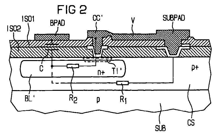
Der Anmeldungsgegenstand betrifft eine Anordnung, bei der die
minimale Rauschzahl dadurch reduziert wird, daß unterhalb der
Basisanschlußfläche eine hoch dotierte vergrabene Schicht
(BL') hergestellt wird, die in der Nähe der Basisanschlußfläche
über einen Standard-Kollektorkontakt (CC') mit Bezugspotential
(GRD) verbunden ist. Vorteilhaft ist hierbei die Senkung
der minimalen Rauschzahl ohne zusätzliche Prozeßschritte.
Applications Claiming Priority (2)
| Application Number | Priority Date | Filing Date | Title |
|---|---|---|---|
| DE19740909A DE19740909C2 (en) | 1997-09-17 | 1997-09-17 | Arrangement for reducing noise in microwave transistors and method for their production |
| DE19740909 | 1997-09-17 |
Publications (2)
| Publication Number | Publication Date |
|---|---|
| EP0903787A2 EP0903787A2 (en) | 1999-03-24 |
| EP0903787A3 true EP0903787A3 (en) | 1999-12-08 |
Family
ID=7842660
Family Applications (1)
| Application Number | Title | Priority Date | Filing Date |
|---|---|---|---|
| EP98116217A Withdrawn EP0903787A3 (en) | 1997-09-17 | 1998-08-27 | Device for reducing noise in microwave transistors and method for its fabrication |
Country Status (4)
| Country | Link |
|---|---|
| US (1) | US6069404A (en) |
| EP (1) | EP0903787A3 (en) |
| JP (1) | JP3973777B2 (en) |
| DE (1) | DE19740909C2 (en) |
Families Citing this family (5)
| Publication number | Priority date | Publication date | Assignee | Title |
|---|---|---|---|---|
| US6612852B1 (en) | 2000-04-13 | 2003-09-02 | Molex Incorporated | Contactless interconnection system |
| US6362972B1 (en) | 2000-04-13 | 2002-03-26 | Molex Incorporated | Contactless interconnection system |
| AU2003217883A1 (en) * | 2002-02-25 | 2003-09-09 | Molex Incorporated | Power delivery to base of processor |
| JP4626935B2 (en) * | 2002-10-01 | 2011-02-09 | ルネサスエレクトロニクス株式会社 | Semiconductor device and manufacturing method thereof |
| US6946720B2 (en) * | 2003-02-13 | 2005-09-20 | Intersil Americas Inc. | Bipolar transistor for an integrated circuit having variable value emitter ballast resistors |
Citations (1)
| Publication number | Priority date | Publication date | Assignee | Title |
|---|---|---|---|---|
| EP0439163A2 (en) * | 1990-01-25 | 1991-07-31 | Kabushiki Kaisha Toshiba | Semiconductor device having a high-frequency bipolar transistor |
Family Cites Families (1)
| Publication number | Priority date | Publication date | Assignee | Title |
|---|---|---|---|---|
| EP0632505B1 (en) * | 1993-07-01 | 1997-10-01 | Co.Ri.M.Me. Consorzio Per La Ricerca Sulla Microelettronica Nel Mezzogiorno | A vertical bipolar power transistor with buried base and interdigitated geometry |
-
1997
- 1997-09-17 DE DE19740909A patent/DE19740909C2/en not_active Expired - Fee Related
-
1998
- 1998-08-27 EP EP98116217A patent/EP0903787A3/en not_active Withdrawn
- 1998-09-16 JP JP26159998A patent/JP3973777B2/en not_active Expired - Fee Related
- 1998-09-17 US US09/156,202 patent/US6069404A/en not_active Expired - Lifetime
Patent Citations (1)
| Publication number | Priority date | Publication date | Assignee | Title |
|---|---|---|---|---|
| EP0439163A2 (en) * | 1990-01-25 | 1991-07-31 | Kabushiki Kaisha Toshiba | Semiconductor device having a high-frequency bipolar transistor |
Non-Patent Citations (1)
| Title |
|---|
| N. CAMILLERI ET AL.: "Bonding pad models for silicon VLSI technologies and their effects on the noise figure of RF NPNs", MICROWAVE AND MILLIMETER-WAVE MONOLITHIC CIRCUITS SYMPOSIUM 1994, DIGEST OF PAPERS, 22 May 1994 (1994-05-22) - 25 May 1994 (1994-05-25), pages 225 - 228, XP002118295 * |
Also Published As
| Publication number | Publication date |
|---|---|
| US6069404A (en) | 2000-05-30 |
| JPH11145152A (en) | 1999-05-28 |
| JP3973777B2 (en) | 2007-09-12 |
| DE19740909A1 (en) | 1999-03-25 |
| DE19740909C2 (en) | 1999-07-01 |
| EP0903787A2 (en) | 1999-03-24 |
Similar Documents
| Publication | Publication Date | Title |
|---|---|---|
| CA1300764C (en) | Semiconductor devices having closely spaced device regions formed using a selfaligning reverse image fabrication process | |
| DE69535441D1 (en) | METHOD FOR PRODUCING A MOS-CONTROLLED COMPONENT WITH A REDUCED MASK NUMBER | |
| EP1109226A3 (en) | Semiconductor device and its manufacturing method capable of reducing low frequency noise | |
| EP0526212A3 (en) | Method of forming isolated regions of oxide | |
| EP1235279A3 (en) | Semiconductor device using nitride compound and method for fabricating the same | |
| EP0736897A3 (en) | Method for forming a trench isolation structure in an integrated circuit | |
| EP1233457A3 (en) | Insulated gate semiconductor device and method of manufacturing the same | |
| EP0984444A3 (en) | Probe and information recording/reproduction apparatus using the same | |
| TW359882B (en) | Bipolar/CMOS integrated circuit | |
| EP0712155A3 (en) | Method for making ohmic contact to lightly doped islands from a silicide buried layer and applications | |
| EP0459397A3 (en) | Semiconductor device having a trench for device isolation and method of fabricating the same | |
| EP0797245A3 (en) | Method of manufacturing a vertical MOS semiconductor device | |
| EP1148557A3 (en) | Stacked capacitor and method of fabricating the stacked capacitor | |
| EP1150349A3 (en) | Process for reduction of orientation-dependent oxidation in trench structures and semiconductor memory device produced thereby | |
| EP1014442A3 (en) | Method for forming a dram capacitor and capacitor made thereby | |
| EP1179863A3 (en) | Organic electronic device, method of producing the same, and method of operating the same | |
| EP0694963A3 (en) | Improvements in BiCMOS semiconductor devices and method therefor | |
| EP0827202A3 (en) | Semiconductor device including protection means and method of fabricating the same | |
| EP0903787A3 (en) | Device for reducing noise in microwave transistors and method for its fabrication | |
| EP0572214A3 (en) | Method for fabricating an interconnect structure in an integrated circuit | |
| EP0665598A3 (en) | Low capacitance floating diffusion structure for a solid state image sensor | |
| EP1164632A3 (en) | Method of forming a fluoro-organosilicate layer on a substrate | |
| EP2096670A3 (en) | Quantum semiconductor device and method for fabricating the same | |
| EP0828290A3 (en) | Method of forming power semiconductor devices with controllable integrated buffer | |
| EP0384396A3 (en) | Bi-cmos semiconductor device having memory cells formed in isolated wells |
Legal Events
| Date | Code | Title | Description |
|---|---|---|---|
| PUAI | Public reference made under article 153(3) epc to a published international application that has entered the european phase |
Free format text: ORIGINAL CODE: 0009012 |
|
| AK | Designated contracting states |
Kind code of ref document: A2 Designated state(s): DE FR GB |
|
| AX | Request for extension of the european patent |
Free format text: AL;LT;LV;MK;RO;SI |
|
| PUAL | Search report despatched |
Free format text: ORIGINAL CODE: 0009013 |
|
| AK | Designated contracting states |
Kind code of ref document: A3 Designated state(s): AT BE CH CY DE DK ES FI FR GB GR IE IT LI LU MC NL PT SE |
|
| AX | Request for extension of the european patent |
Free format text: AL;LT;LV;MK;RO;SI |
|
| 17P | Request for examination filed |
Effective date: 20000105 |
|
| AKX | Designation fees paid |
Free format text: DE FR GB |
|
| RAP1 | Party data changed (applicant data changed or rights of an application transferred) |
Owner name: INFINEON TECHNOLOGIES AG |
|
| STAA | Information on the status of an ep patent application or granted ep patent |
Free format text: STATUS: THE APPLICATION HAS BEEN WITHDRAWN |
|
| 18W | Application withdrawn |
Effective date: 20040414 |