EP0903754A2 - Nicht-flüchtige Halbleiter-Speicher-Vorrichtung - Google Patents
Nicht-flüchtige Halbleiter-Speicher-Vorrichtung Download PDFInfo
- Publication number
- EP0903754A2 EP0903754A2 EP98121759A EP98121759A EP0903754A2 EP 0903754 A2 EP0903754 A2 EP 0903754A2 EP 98121759 A EP98121759 A EP 98121759A EP 98121759 A EP98121759 A EP 98121759A EP 0903754 A2 EP0903754 A2 EP 0903754A2
- Authority
- EP
- European Patent Office
- Prior art keywords
- verify
- source voltage
- voltage
- semiconductor memory
- nonvolatile semiconductor
- Prior art date
- Legal status (The legal status is an assumption and is not a legal conclusion. Google has not performed a legal analysis and makes no representation as to the accuracy of the status listed.)
- Granted
Links
Images




Classifications
-
- G—PHYSICS
- G11—INFORMATION STORAGE
- G11C—STATIC STORES
- G11C16/00—Erasable programmable read-only memories
- G11C16/02—Erasable programmable read-only memories electrically programmable
- G11C16/06—Auxiliary circuits, e.g. for writing into memory
- G11C16/26—Sensing or reading circuits; Data output circuits
-
- G—PHYSICS
- G11—INFORMATION STORAGE
- G11C—STATIC STORES
- G11C16/00—Erasable programmable read-only memories
- G11C16/02—Erasable programmable read-only memories electrically programmable
- G11C16/06—Auxiliary circuits, e.g. for writing into memory
- G11C16/30—Power supply circuits
-
- G—PHYSICS
- G11—INFORMATION STORAGE
- G11C—STATIC STORES
- G11C29/00—Checking stores for correct operation ; Subsequent repair; Testing stores during standby or offline operation
- G11C29/04—Detection or location of defective memory elements, e.g. cell constructio details, timing of test signals
-
- G—PHYSICS
- G11—INFORMATION STORAGE
- G11C—STATIC STORES
- G11C29/00—Checking stores for correct operation ; Subsequent repair; Testing stores during standby or offline operation
- G11C29/52—Protection of memory contents; Detection of errors in memory contents
-
- G—PHYSICS
- G06—COMPUTING OR CALCULATING; COUNTING
- G06F—ELECTRIC DIGITAL DATA PROCESSING
- G06F2201/00—Indexing scheme relating to error detection, to error correction, and to monitoring
- G06F2201/81—Threshold
Definitions
- This invention relates to a nonvolatile semiconductor memory, particularly to an EPROM and an EEPROM including a nonvolatile memory circuit and, more particularly to a circuit construction of a nonvolatile semiconductor memory of the batch erasure type (hereinafter referred to as a flash memory).
- the invention further relates particularly to a circuit construction concerning a sense amplifying (S/A) circuit and supply of a supply voltage in a nonvolatile semiconductor memory.
- S/A sense amplifying
- Fig. 8 of the accompanying drawings shows diagrammatically a structure of a cell used in a flash memory.
- V G is a gate terminal, at V D a drain terminal, at V S a source terminal, at 27 a control gate CG connected to the gate terminal V G , and at 25 a floating gate FG which is controlled by the potential of the control gate CG.
- a semiconductor substrate e.g. a semiconductor substrate having P-type conductivity.
- well portions 23, 24 made of semiconductor having N-type conductivity.
- the well portion 23 forms a drain while the well portion 24 forms a source.
- Indicated at 26, 28 are insulating films.
- the write verification and erase verification are carried out so as to confirm whether the degree of writing and the degree of erasing have a sufficient margin for the read voltage, i.e., a variation range of the normal supply voltage V CC (5V ⁇ 0.5V). Generally, these verifications are carried out to confirm that an operation margin of about 0.5V to 1.0V is available for a voltage range of V CC . In this case, the verify voltage including the operation margin is 6V to 6.5V in the write verification, and 3.5V to 4V in the erase verification.
- the write verification and the erase verification can be accomplished easily if the verify voltage including the operation margin to be secured is applied to word lines (for example, word lines WL l to WL m of the flash memory shown in Fig. 1), so that the sensitivity of the S/A circuit is the same regardless of whether the voltage V CC or the verify voltage is applied as the supply voltage of the S/A circuit.
- word lines for example, word lines WL l to WL m of the flash memory shown in Fig. 1
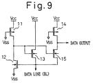
- Fig. 9 of the accompanying drawings shows a construction of a general S/A circuit used in the nonvolatile semiconductor memory such as an EPROM.
- V CC is a line of a supply voltage 5V
- V SS a line of a supply voltage 0V.
- a gate of the transistor 11 is connected to power supply line V SS
- a gate of the transistor 12 is connected to a data line (i.e. a bit line).
- a data line i.e. a bit line.
- an n-channel transistor 13 whose gate is connected to drains of the respective transistors 11, 12.
- a p-channel transistor 14 and an n-channel transistor 15 in series.
- a gate of the transistor 14 is connected to the power supply line V SS
- a gate of the transistor 15 is connected to the drains of the respective transistors 11, 12.
- An output (data output) of the S/A circuit is taken from drains of the respective transistors 14, 15.
- the transistor 15 is provided with a function of transmitting the level of the bit line to the data output line (bit line level adjustment), and the transistor 14 is provided with a function of discriminating the data of the memory cell according to the state (on/off) of the transistor 15.
- the sensitivity of the S/A circuit becomes dependent on the voltage V cc since the voltage V cc is used as a supply voltage, thus presenting the problem that an original object of the verification cannot be accomplished.
- the desired object can be accomplished if the voltage V cc is replaced by the verify voltage.
- the size, i.e. the current supplying performance of a power supply circuit for supplying the verify voltage is disadvantageously required to be increased.
- An embodiment of the present invention seeks to provide a nonvolatile semiconductor memory in which an S/A circuit is permitted to have the sensitivity compatible with any of a write verification and an erase verification even if a normal supply voltage is used, that is, a verification can be conducted sufficiently.
- a nonvolatile semiconductor memory comprising a cell matrix circuit (1) having erasable nonvolatile memory cell transistors (M ij ) arranged at intersections of a plurality of word lines (WL l to WL m ) and a plurality of bit lines (BL ll to BL lk , ..., BL nl to BL nk ); a row decoding circuit (3); a column decoding circuit (5); and sense amplifying circuits (7 l to 7 n ) connected to the respective bit lines (BL ll to BL lk , ..., BL nl to BL nk ) of the cell matrix circuit (1).
- M ij erasable nonvolatile memory cell transistors
- An external power source has a normal source voltage generating means and a specific verify source voltage generating means, independent of one another so that the circuitry of the memory can carry out predetermined operations according to any one of the normal source voltage and the specific verify source voltage in response to a predetermined selection signal.
- the nonvolatile semiconductor memory comprises a cell matrix including erasable nonvolatile memory cells arranged at the intersections of the plurality of word lines and the plurality of bit lines, and sense amplifying (S/A) circuits having two different kinds of source voltages supplied thereto and adapted to apply sense amplification to data of the selected line in the cell matrix.
- the nonvolatile semiconductor memory in this embodiment is provided with external source voltage supplying means having a normal source voltage generating circuit and also having a specific verify source voltage generating circuit capable of generating a source voltage different from the normal source voltage in the write verify operation and the erase verify operation, respectively.
- the two different kinds of source voltages i.e. the normal source voltage and a specific verify source voltage different from the normal source voltage
- the specific verify source voltage different from the normal source voltage V cc is applied to the S/A circuit during the write verification or erase verification, and also to the selected word line. Accordingly, the sensitivity of the S/A circuit to the normal source voltage during a reading operation can be made equal to that of the S/A circuit to the verify source voltage during the verification. Further, margins during a data writing operation and an erasing operation can be checked sufficiently.
- the specific verify source voltage generating circuit in the external source voltage supplying means is used to reduce or boost an external source voltage of, e.g., 5V, to a specified verify source voltage level V VER .
- the size of the verify source voltage generating circuit is determined by the places to which the verify source voltage needs to be supplied. Accordingly, a preferred feature of the invention is to limit the places where the verify source voltage is supplied.
- the reading operation can be executed in the same state as in the prior art by supplying the verify source voltage to limited places. This enables a capacity of the external verify source voltage supply circuit to be small.
- Any one of the normal source voltage and the specific verify source voltage can be selected by a predetermined controlling signal.
- Fig. 1 is a block diagram showing parts of an overall construction of a flash type memory as a specific example of a nonvolatile semiconductor memory embodying the present invention.
- indicated at 1 is a cell array formed by arranging erasable nonvolatile memory cells M ij at intersections of a plurality of word lines WL l to WL m and a plurality of bit lines BL ll to BL lk , ..., BL nl to BL nk .
- the cell array is divided into n blocks, in each of which (k ⁇ m) memory cells are arranged.
- Indicated at 2 is a row address buffer for buffering a row address RAD of an address signal fed externally thereto, at 3 a row decoder for decoding the row address and selecting any one of the word lines WL l to WL m , at 4 a column address buffer for buffering a column address CAD of the address signal, and at 5 a column decoder for decoding the column address and selecting any one of column lines CL l to CL k corresponding to the bit lines BLi l to BLi k for each of the aforementioned blocks.
- Indicated at 6 is a column gate circuit including transfer gate transistors Q l to Q k corresponding to the bit lines BL il to BL ik for each of the aforementioned blocks. The respective transistors Q l to Q k are turned on when the corresponding column lines CL l to CL k are selected, to thereby connect the selected bit line BL ij to a data line D i .
- Indicated at 7 l to 7 n are respectively writing circuits and S/A circuits for applying amplification to a write data and sense amplification to a read data between corresponding internal data lines D l to D n and external input/output data lines I/O l , to I/O n .
- Indicated at 8 is a verify source voltage generating circuit (part of external power source means) for generating a verify voltage V VER in accordance with a control signal C fed externally thereto. The generated verify source voltage V VER is supplied to the selected word lines WL l to WL m through the row decoder 3 as described later, and to the S/A circuit corresponding to the selected word line.
- a source voltage supply circuit for supplying a source voltage in common to the respective voltage V E lower than the normal source voltage (V CC ) and to set the write verify source voltage V W higher than the normal source voltage (V CC ).
- the normal supply voltage (V CC ) is an intermediate value between a first verify voltage which is the erase verify voltage and a second verify voltage which is the write verify voltage.
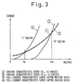
- the desirable range of the write verify source voltage V W and the erase verify source voltage V E can be determined with reference to the graphs as shown in Fig. 3.
- the transistor 34 is turned on.
- the potential at the node of the resistors 31, 32 i.e. the voltage of 6.5V
- the transistor 35 is turned on.
- the potential at the node of the resistors 32, 33 i.e. the voltage of 3.5V
- the potential at the node of the resistors 32, 33 i.e. the voltage of 3.5V
- the transistors 34, 35 are cut off. As a result, only the current mirror circuit operates and an intermediate level (5V) between 6.5V and 3.5V is output as the output voltage V VER . This output voltage is at the same level as the normal supply voltage V CC .
- an output signal of the S/A circuit is normally a weak signal in terms of the amplitude and drive ability, it is preferable to provide a buffer circuit for the purpose of stabilizing the output signal.
- the verify voltage V VER in which the voltage is changed from the bit line potential (about 1V) to the verify voltage V VER during the verification, it is preferable to supply the verify voltage V VER as a source voltage of the buffer circuit.
- Fig. 5 shows an example of a construction of the S/A circuit including a buffer circuit.
- the illustrated circuit is obtainable by adding the buffer circuit to the construction of Fig. 2.
- This buffer circuit includes a p-channel transistor 16 and n-channel transistors 17, 18 which are connected in series between the verify source voltage line V VER and the power supply line V SS and which are responsive to the drain potentials of the respective transistors 14, 15; and a p-channel transistor 19 which is connected between the voltage line V VER and a connection node between the transistors 17, 18 and which is responsive to the drain potentials of the respective transistors 14, 15.
- the output of the S/A circuit (data output) is taken from the drains of the respective transistors 16, 17.
- the sense characteristic curves shown in Fig. 3 are ideally required to be devised.
- the inclination of the sense characteristic curve is preferably large in the neighborhood of the write verify source voltage V W so that a large power supply margin is taken for a change of a threshold voltage of the cell transistor.
- the inclination of the sense characteristic curve is preferably small in the neighborhood of the erase verify source voltage V E so as to make it easier to adjust the voltage V E finely and in order to improve the stability of the characteristic in terms of differences among cell transistors.
- Fig. 6 shows ideal sense characteristic curves
- Fig. 7 shows an example of a construction of a preferable S/A circuit for realizing this characteristic.
- the illustrated circuit is obtainable by adding two transistors 20 and 21 to the construction of the S/A circuit including the buffer circuit shown in Fig. 5.
- the transistor 20 is a p-channel transistor, and is connected between the verify source voltage V VER and the source of the transistor 14. A gate of the transistor 20 is connected to a drain thereof. Accordingly, this transistor 20 functions as a voltage reducing element.
- the transistor 21 is an n-channel transistor of the depletion type, and is connected between the voltage V VER and the commonly-connected drains of the transistors 14,15. A gate of the transistor 21 is connected to a source thereof. Accordingly, this transistor 21 functions as a constant current supplying element.
- the portion of the overall memory circuit to which the verify source voltage should be applied may be confined just to the selected word line and the transistor used for comparing with a voltage level provided in the sense amplifier.
- the number of the portions to which the verify source voltage should be applied in the verify operation can be significantly reduced as compared with the conventional method in which the source voltage V CC applied to each of the components provided in the memory circuit is simply and uniformly converted to the verify source voltage. Accordingly, in the present invention, the number of the circuit elements to which the source voltage should be applied is remarkably small, thereby making it possible to reduce the performance required of the verify source voltage generating circuit used for supplying the verify source voltage. Accordingly, this generating circuit can be made significantly smaller than the comparable generating circuit required by the conventional method and thus the area to be occupied by the verify source voltage generating circuit can be significantly reduced whilst still maintaining suitable sensitivity in the verifying operation.
Landscapes
- Read Only Memory (AREA)
- Semiconductor Memories (AREA)
- Non-Volatile Memory (AREA)
Applications Claiming Priority (4)
| Application Number | Priority Date | Filing Date | Title |
|---|---|---|---|
| JP34666391 | 1991-12-27 | ||
| JP3346663A JP2732471B2 (ja) | 1991-12-27 | 1991-12-27 | 不揮発性半導体記憶装置 |
| JP346663/91 | 1991-12-27 | ||
| EP92311829A EP0549374B1 (de) | 1991-12-27 | 1992-12-29 | Nicht-flüchtiger Halbleiterspeicher |
Related Parent Applications (1)
| Application Number | Title | Priority Date | Filing Date |
|---|---|---|---|
| EP92311829A Division EP0549374B1 (de) | 1991-12-27 | 1992-12-29 | Nicht-flüchtiger Halbleiterspeicher |
Publications (3)
| Publication Number | Publication Date |
|---|---|
| EP0903754A2 true EP0903754A2 (de) | 1999-03-24 |
| EP0903754A3 EP0903754A3 (de) | 1999-04-28 |
| EP0903754B1 EP0903754B1 (de) | 2002-09-18 |
Family
ID=18384972
Family Applications (1)
| Application Number | Title | Priority Date | Filing Date |
|---|---|---|---|
| EP98121759A Expired - Lifetime EP0903754B1 (de) | 1991-12-27 | 1992-12-29 | Nicht-flüchtige Halbleiter-Speicher-Vorrichtung |
Country Status (3)
| Country | Link |
|---|---|
| EP (1) | EP0903754B1 (de) |
| JP (1) | JP2732471B2 (de) |
| DE (1) | DE69232785T2 (de) |
Families Citing this family (3)
| Publication number | Priority date | Publication date | Assignee | Title |
|---|---|---|---|---|
| US5396468A (en) * | 1991-03-15 | 1995-03-07 | Sundisk Corporation | Streamlined write operation for EEPROM system |
| KR100463954B1 (ko) * | 2002-05-17 | 2004-12-30 | 주식회사 하이닉스반도체 | 플래시 메모리 장치 및 그 소거 방법 |
| JP5191834B2 (ja) * | 2008-08-12 | 2013-05-08 | セイコーインスツル株式会社 | 半導体不揮発性記憶装置 |
Family Cites Families (5)
| Publication number | Priority date | Publication date | Assignee | Title |
|---|---|---|---|---|
| JPS62222498A (ja) * | 1986-03-10 | 1987-09-30 | Fujitsu Ltd | 消去及び書き込み可能な読み出し専用メモリ |
| JPS63291297A (ja) * | 1987-05-22 | 1988-11-29 | Nec Corp | 書込み及び消去可能な不揮発性メモリ− |
| JPH0787039B2 (ja) * | 1987-12-28 | 1995-09-20 | 株式会社東芝 | 不揮発性半導体記憶装置 |
| US4875188A (en) * | 1988-01-12 | 1989-10-17 | Intel Corporation | Voltage margining circuit for flash eprom |
| US5172338B1 (en) * | 1989-04-13 | 1997-07-08 | Sandisk Corp | Multi-state eeprom read and write circuits and techniques |
-
1991
- 1991-12-27 JP JP3346663A patent/JP2732471B2/ja not_active Expired - Fee Related
-
1992
- 1992-12-29 DE DE69232785T patent/DE69232785T2/de not_active Expired - Fee Related
- 1992-12-29 EP EP98121759A patent/EP0903754B1/de not_active Expired - Lifetime
Also Published As
| Publication number | Publication date |
|---|---|
| JPH05182478A (ja) | 1993-07-23 |
| EP0903754B1 (de) | 2002-09-18 |
| DE69232785D1 (de) | 2002-10-24 |
| DE69232785T2 (de) | 2003-02-20 |
| JP2732471B2 (ja) | 1998-03-30 |
| EP0903754A3 (de) | 1999-04-28 |
Similar Documents
| Publication | Publication Date | Title |
|---|---|---|
| JP3783885B2 (ja) | 不揮発性半導体メモリ装置 | |
| JP2732826B2 (ja) | 不揮発性半導体メモリ装置とそのワードライン駆動方法 | |
| US5388069A (en) | Nonvolatile semiconductor memory device for preventing erroneous operation caused by over-erase phenomenon | |
| US8339852B2 (en) | Non-volatile memory device | |
| US6788601B2 (en) | Semiconductor memory device and current mirror circuit | |
| US6816413B2 (en) | Nonvolatile semiconductor memory capable of generating read-mode reference current and verify-mode reference current from the same reference cell | |
| US20050036369A1 (en) | Temperature compensated bit-line precharge | |
| JP3920943B2 (ja) | 不揮発性半導体記憶装置 | |
| JP2001057088A (ja) | Nand型不揮発性メモリ | |
| US6229734B1 (en) | Nonvolatile semiconductor storage device having controlled cell threshold voltage distribution | |
| US6947325B2 (en) | Non-volatile semiconductor memory device and controlling method of the same | |
| US7453742B2 (en) | Semiconductor integrated circuit device | |
| EP0241327A2 (de) | Leseverstärker für programmierbaren Festwertspeicher | |
| US5708602A (en) | Non-volatile semiconductor memory device and method for verifying operating of the same | |
| US5729162A (en) | Integrated circuit memory with column voltage holding circuit | |
| US5812451A (en) | Nonvolatile semiconductor storage apparatus and method of writing data to the same | |
| JP2005032430A (ja) | フラッシュメモリ装置 | |
| US20090296480A1 (en) | Circuit for generating a voltage and a non-volatile memory device having the same | |
| US6535427B1 (en) | Nonvolatile semiconductor memory device with initialization circuit and control method thereof | |
| US7315475B2 (en) | Non-volatile semiconductor memory device | |
| US7529133B2 (en) | Nonvolatile semiconductor storage apparatus and readout method | |
| JP2009295221A (ja) | 半導体記憶装置 | |
| US5398204A (en) | Nonvolatile semiconductor system | |
| US5808935A (en) | Common source line driving circuit for use in nonvolatile semiconductor memories | |
| EP0903754B1 (de) | Nicht-flüchtige Halbleiter-Speicher-Vorrichtung |
Legal Events
| Date | Code | Title | Description |
|---|---|---|---|
| PUAI | Public reference made under article 153(3) epc to a published international application that has entered the european phase |
Free format text: ORIGINAL CODE: 0009012 |
|
| PUAL | Search report despatched |
Free format text: ORIGINAL CODE: 0009013 |
|
| AC | Divisional application: reference to earlier application |
Ref document number: 549374 Country of ref document: EP |
|
| AK | Designated contracting states |
Kind code of ref document: A2 Designated state(s): DE FR GB IT |
|
| AK | Designated contracting states |
Kind code of ref document: A3 Designated state(s): DE FR GB IT |
|
| 17P | Request for examination filed |
Effective date: 19990922 |
|
| 17Q | First examination report despatched |
Effective date: 20010205 |
|
| GRAG | Despatch of communication of intention to grant |
Free format text: ORIGINAL CODE: EPIDOS AGRA |
|
| GRAG | Despatch of communication of intention to grant |
Free format text: ORIGINAL CODE: EPIDOS AGRA |
|
| GRAH | Despatch of communication of intention to grant a patent |
Free format text: ORIGINAL CODE: EPIDOS IGRA |
|
| GRAH | Despatch of communication of intention to grant a patent |
Free format text: ORIGINAL CODE: EPIDOS IGRA |
|
| GRAA | (expected) grant |
Free format text: ORIGINAL CODE: 0009210 |
|
| AC | Divisional application: reference to earlier application |
Ref document number: 549374 Country of ref document: EP |
|
| AK | Designated contracting states |
Kind code of ref document: B1 Designated state(s): DE FR GB IT |
|
| REG | Reference to a national code |
Ref country code: GB Ref legal event code: FG4D |
|
| REF | Corresponds to: |
Ref document number: 69232785 Country of ref document: DE Date of ref document: 20021024 |
|
| ET | Fr: translation filed | ||
| PLBE | No opposition filed within time limit |
Free format text: ORIGINAL CODE: 0009261 |
|
| STAA | Information on the status of an ep patent application or granted ep patent |
Free format text: STATUS: NO OPPOSITION FILED WITHIN TIME LIMIT |
|
| 26N | No opposition filed |
Effective date: 20030619 |
|
| PGFP | Annual fee paid to national office [announced via postgrant information from national office to epo] |
Ref country code: GB Payment date: 20071227 Year of fee payment: 16 Ref country code: FR Payment date: 20071210 Year of fee payment: 16 |
|
| PGFP | Annual fee paid to national office [announced via postgrant information from national office to epo] |
Ref country code: IT Payment date: 20071228 Year of fee payment: 16 Ref country code: DE Payment date: 20071231 Year of fee payment: 16 |
|
| GBPC | Gb: european patent ceased through non-payment of renewal fee |
Effective date: 20081229 |
|
| REG | Reference to a national code |
Ref country code: FR Ref legal event code: ST Effective date: 20090831 |
|
| PG25 | Lapsed in a contracting state [announced via postgrant information from national office to epo] |
Ref country code: DE Free format text: LAPSE BECAUSE OF NON-PAYMENT OF DUE FEES Effective date: 20090701 |
|
| PG25 | Lapsed in a contracting state [announced via postgrant information from national office to epo] |
Ref country code: GB Free format text: LAPSE BECAUSE OF NON-PAYMENT OF DUE FEES Effective date: 20081229 |
|
| PG25 | Lapsed in a contracting state [announced via postgrant information from national office to epo] |
Ref country code: FR Free format text: LAPSE BECAUSE OF NON-PAYMENT OF DUE FEES Effective date: 20081231 |
|
| PG25 | Lapsed in a contracting state [announced via postgrant information from national office to epo] |
Ref country code: IT Free format text: LAPSE BECAUSE OF NON-PAYMENT OF DUE FEES Effective date: 20081229 |