EP0902462A1 - Verfahren zur Herstellung einer Unterelektrode für eine Halbleiterspeichervorrichtung - Google Patents
Verfahren zur Herstellung einer Unterelektrode für eine Halbleiterspeichervorrichtung Download PDFInfo
- Publication number
- EP0902462A1 EP0902462A1 EP97306946A EP97306946A EP0902462A1 EP 0902462 A1 EP0902462 A1 EP 0902462A1 EP 97306946 A EP97306946 A EP 97306946A EP 97306946 A EP97306946 A EP 97306946A EP 0902462 A1 EP0902462 A1 EP 0902462A1
- Authority
- EP
- European Patent Office
- Prior art keywords
- lower electrode
- amorphous silicon
- memory device
- manufacturing
- semiconductor memory
- Prior art date
- Legal status (The legal status is an assumption and is not a legal conclusion. Google has not performed a legal analysis and makes no representation as to the accuracy of the status listed.)
- Granted
Links
Images


Classifications
-
- H—ELECTRICITY
- H10—SEMICONDUCTOR DEVICES; ELECTRIC SOLID-STATE DEVICES NOT OTHERWISE PROVIDED FOR
- H10D—INORGANIC ELECTRIC SEMICONDUCTOR DEVICES
- H10D1/00—Resistors, capacitors or inductors
- H10D1/60—Capacitors
- H10D1/68—Capacitors having no potential barriers
- H10D1/692—Electrodes
- H10D1/711—Electrodes having non-planar surfaces, e.g. formed by texturisation
- H10D1/712—Electrodes having non-planar surfaces, e.g. formed by texturisation being rough surfaces, e.g. using hemispherical grains
Definitions
- the present invention relates to a semiconductor device manufacturing method, and more particularly, to a method for manufacturing a capacitor lower electrode of a semiconductor memory device which increases capacitor capacitance by increasing the surface area of the electrode in a dynamic random access memory (DRAM).
- DRAM dynamic random access memory
- the cell capacitance of a semiconductor memory device is an important factor in determining the memory capacity thereof.
- the capacitance can be increased by varying three parameters, i.e., the dielectric constant of a dielectric film, the effective area of a capacitor, or the thickness of the dielectric film.
- a hemispherical grain (HSG) silicon film is formed as a rugged surface on the surface of a lower electrode, or a three-dimensional capacitor structure is used, including a stack, a trench, and a cylindrical structure.
- Tatsumi discloses in U.S. Patent No. 5,385,863 that , in order to increase the effective area of the capacitor electrode, a capacitance electrode made of a polysilicon film is formed, the polysilicon film being formed by depositing an amorphous silicon film on an insulating film covering a semiconductor substrate, generating a plurality of crystal nuclei at a plurality of the amorphous silicon film, respectively, and growing each of the plurality of crystal nuclei into a mushroom or hemisphere shaped crystal grain to thereby convert the amorphous silicon film into the polysilicon film.
- FIGS. 1A and 1B are scanning electron microscope (SEM) photos showing the result of forming HSGs on a partially crystallized amorphous silicon film on a semiconductor substrate.
- SEM scanning electron microscope
- the amorphous silicon surface is contaminated by foreign materials and thus the amorphous silicon atoms are combined with foreign atoms, it is difficult for the silicon to make a surface migration, the amorphous silicon surface is further contaminated, and crystal nucleation and growth is terminated if the foreign materials are accumulated to a predetermined thickness.
- a method for manufacturing a capacitor lower electrode of a semiconductor memory device comprises the steps of:
- the supply of the predetermined gas is performed while heating the semiconductor substrate, and the step of heating the semiconductor substrate comprises the steps of: (a) maintaining the temperature of the susceptor at 700-1000°C for 5-40 seconds; and (b) maintaining the temperature of the susceptor at 500-800°C in the process chamber, immediately after the step (a).
- the predetermined gas is one of SiH 4 , Si 2 H 6 , SiH 2 Cl 2 , and a mixture thereof. More preferably, the predetermined gas further comprises an inert gas.
- the amorphous silicon thin layer is selectively deposited only on the surface of the lower electrode pattern in the step of (e).
- step of (f) is performed without vacuum breakdown subsequent to the step of (e), and the step of (f) is performed at a pressure of 10 -7 torr or below.
- the step of (f) comprises the sub steps of: continuously supplying the predetermined gas during the silicon crystal nuclei formation; and blocking the supply of the predetermined gas during the silicon crystal nuclei growth.
- the supply of the predetermined gas is simultaneously controlled in the step of supplying a predetermined gas.
- HSG silicon film to increase the effective area of the electrode relies on the mechanism of surface migration of silicon atoms.
- crystal nuclei are formed on the surface of an amorphous silicon film using a silicon source gas, e.g., silane (SiH 4 ) or disilane (Si 2 H 6 ) gas, and annealed so that silicon atoms of the amorphous silicon film migrate to the crystal nuclei and form a HSG silicon film having hemispherical grains of a predetermined size on the surface of the amorphous silicon film.
- a silicon source gas e.g., silane (SiH 4 ) or disilane (Si 2 H 6 ) gas
- the migration time of the silicon atoms to the crystal nuclei should exceed the crystallization time of a bulk area of the amorphous silicon film being an underlayer. Therefore, the migration time and the crystallization time should be stably controlled to ensure the increase of the effective area of the electrode by the above mechanism.
- the mechanism of forming the HSG silicon film as a rugged surface on the surface of the amorphous silicon film is affected by two factors during processing: the characteristics of the amorphous silicon film itself and contamination caused by foreign materials adsorbed on the surface of the underlayer before or after crystal nucleation.
- the amorphous silicon film used as an underlayer to form the rugged surface should be kept amorphous and completely free of crystal grains.
- the possible existence of the crystal grains in the underlayer prevents silicon atoms of the crystal grains from migrating to the crystal nuclei during formation of the rugged surface.
- foreign material-induced contamination may occur in cleaning the surface of the underlayer or exposing a resultant including the crystal nuclei to the atmosphere.
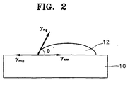
- FIG. 2 illustrates a typical crystal nucleus 12 formed of crystal silicon on the surface of a lower amorphous silicon electrode pattern 10 in a gaseous atmosphere.
- phase transition-related Gibbs free energy and interface energy i.e., surface energy generated during crystal nucleation and growth.
- G (4/3) ⁇ r 2 ⁇ G tr f( ⁇ ) + 4 ⁇ r 2 ⁇ f( ⁇ )
- ⁇ G the total Gibbs free energy
- r the radius of a crystal nucleus
- ⁇ G tr the Gibbs free energy of phase transition per unit volume
- ⁇ is the vector sum of ⁇ mg , ⁇ nm , and ⁇ ng , which are the surface tensions between gas and amorphous silicon, between crystal silicon and amorphous silicon, and between gas and crystal silicon, respectively.
- f( ⁇ ) is a configuration factor.
- the silicon atoms on the surface of the amorphous silicon migrate to the crystal silicon, that is, the crystal nucleus 12, with activation energy given by the above equation so that crystal nuclei are grown.
- the above equation represents the minimum activation energy needed for the growth of the silicon atoms in the amorphous silicon film into crystal silicon through the phase-transition to the crystal silicon nucleus.
- the silicon atoms of the amorphous silicon film should migrate to the crystal silicon for the growth of the crystal nucleus.
- the amorphous silicon should be kept amorphous condition and have a free surface in which silicon atoms are not combined with other atoms.
- a semiconductor substrate having an amorphous silicon layer formed thereon is loaded in a process chamber and an amorphous silicon thin layer of high purity and few defects is formed on the amorphous silicon layer in an ultrahigh vacuum state. Subsequently, crystal nucleation and growth are performed on the amorphous silicon thin layer, thereby forming an intended rugged surface.
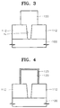
- FIGS. 3 through 6 are sectional views sequentially showing the steps in a method for manufacturing a capacitor of a semiconductor memory device according to a preferred embodiment of the present invention.
- an insulation layer is formed on a semiconductor substrate 100 including an underlying structure such as a transistor to insulate the underlying structure. Then, a photoresist pattern (not shown) is formed on the insulation layer by photolithography. The insulation layer is etched using the photoresist pattern as an etching mask, thereby forming an insulation pattern 112 and a contact hole h 1 for exposing a portion of the semiconductor substrate 100.
- an impurity-doped amorphous silicon film is deposited on the overall surface of the resultant having the contact hole h 1 .
- a lower electrode pattern 120 of amorphous silicon is formed by patterning the deposited amorphous silicon film.
- the resultant is loaded in the process chamber (not shown) kept in a ultrahigh vacuum state, preferably, below or at a pressure of 10 -7 torr.
- FIG. 7 is a graph showing a temperature variation in each stage during processing in the process chamber to form the rugged surface on the lower electrode pattern 120 of the semiconductor substrate 100.
- reference character (a) indicates a variation in a setting temperature of a heater installed in the chamber to control the temperature of a susceptor in the process chamber.
- Reference character (b) indicates a variations in semiconductor substrate temperature actually observed.
- Reference character (c) indicates a variation in susceptor temperature.
- the susceptor is heated to 700-1000°C, preferably about 850°C, by increasing the heater temperature to approximately 1000°C for about 5-40 seconds, preferably 20 seconds, so as to rapidly increase the temperature of the semiconductor substrate 100 having the lower electrode pattern 120 formed thereon loaded in the process chamber. Then, the susceptor temperature is reduced to a predetermined temperature, for example, 500-800°C, preferably 720°C, by decreasing the heater temperature to about 765°C, and then the heater temperature is maintained at about 765°C.
- the semiconductor substrate 100 is kept in the process chamber for a predetermined time until the surface of the lower electrode pattern 120 is set at a temperature appropriate for depositing an amorphous silicon thin layer thereon in a subsequent process.
- a standby time that is, time required to reach a temperature suitable for the deposition of the amorphous silicon thin layer, is referred to as a temperature stabilizing time.
- the process chamber is supplied with a process gas needed to form crystal nuclei for rugged surface formation, for example, one of SiH 4 , Si 2 H 6 , and SiH 2 Cl 2 , so as to deposit the amorphous silicon thin layer on the surface of the lower electrode pattern 120.
- a process gas needed to form crystal nuclei for rugged surface formation, for example, one of SiH 4 , Si 2 H 6 , and SiH 2 Cl 2 , so as to deposit the amorphous silicon thin layer on the surface of the lower electrode pattern 120.
- an inert gas such as nitrogen (N 2 ) or argon (Ar) can be simultaneously supplied into the process chamber.
- FIG. 4 illustrates the amorphous silicon thin layer 125 deposited on the surface of the lower electrode pattern 120.
- the amorphous silicon thin layer 125 is deposited to a thickness of several tens of angstroms, preferably, only on the surface of the lower electrode pattern 120 by controlling the process gas supply time.
- the process chamber is kept at near vacuum conditions of 10 -3 torr or below even during the deposition of the amorphous silicon thin layer 125, the adsorption of impurities on the surface of the lower electrode pattern 120 is prevented, thus suppressing contamination of the surface of the semiconductor substrate.
- the substrate temperature is heated to a temperature to allow crystal nuclei formation, for example, 570°C or above.
- a plurality of crystal nuclei can be formed on the surface of the amorphous silicon thin layer 125.
- stage 3 of FIG. 7 as the semiconductor substrate 100 is gradually heated to a crystallization temperature or above, a plurality of crystal nuclei are successively formed on the amorphous silicon thin layer 125 (see FIG. 4). That is, the crystal nuclei are formed on the amorphous silicon thin layer 125 without vacuum breakdown, subsequent to the deposition of the amorphous silicon thin layer 125 in high vacuum.
- the aforementioned process is continuously provided.
- the flow of gas may be simultaneously controlled. Therefore, adsorption and generation of impurities at their interface can be prevented by sequential formation of the amorphous silicon thin layer 125 and the silicon crystal nuclei without vacuum breakdown. Therefore, crystal nuclei of a uniform configuration can be formed in the method of the present invention.
- stage 4 of FIG. 7 supply of the process gas is terminated, and the pressure of the process chamber is maintained again in ultrahigh vacuum, for example, below or at 10 -7 Torr, and a process for crystal nuclei growth is performed. That is, as the temperature of the semiconductor substrate 100 reaches a steady-state temperature in the process chamber, crystal nuclei 128 are in effect subjected to heat treatment at the silicon crystallization temperature or above. In practice, it takes approximately 150 seconds for the semiconductor substrate 100 to reach a steady state, i.e., about 600°C in the process chamber. At this time period, silicon atoms in the amorphous silicon thin layer 125 migrate to the crystal nuclei 128 so that crystal nuclei 128 can be grown.
- the growth of the grains should be controlled by adjusting the heat treatment temperature and time to allow a rugged surface having grains of an appropriate size to be formed.
- FIG. 6 is a sectional view of a completed lower electrode 130 having a rugged surface.
- reference numeral 120A indicates the outline of the lower electrode pattern 120 before completing the rugged surface on the lower electrode 130.
- the semiconductor substrate 100 is unloaded from the process chamber and cooled to room temperature.
- a capacitor insulation film is formed on the above resultant and a conductive material is deposited on the capacitor insulation film to form an upper electrode.
- a series of processes for forming the amorphous silicon thin layer on the surface of the lower electrode pattern, forming crystal nuclei and forming the rugged surface are successively performed in the process chamber without vacuum breakdown, thus enabling processing in a highly clean state. Accordingly, the drawbacks encountered in the prior art such as failure of growth of the crystal grains can be overcome and uniformity of crystal grain size and density can be increased. Furthermore, deposition of the amorphous layer between the lower electrode and the rugged surface decreases the ratio of the minimum value to the maximum value of a capacitance (hereinafter, referred to as Cmin/Cmax). This problem can be solved without an additional heat treatment for an ideal Cmin/Cmax, since the semiconductor substrate is subjected to heat treatment in effect in a subsequent process to the formation of a capacitor.
- the characteristics of a capacitor having a rugged surface on a lower electrode according to the method of the present invention are estimated as follows.
- a temperature stabilization time that is, a standby time before supply of a process gas needed to form the amorphous silicon thin layer, was varied from between 30-180 seconds and a process gas supply time was varied from between 80-140 seconds, with the conditions of a heater temperature of 765°C, a crystal nuclei growth time of 180 seconds, and process gad Si 2 H 6 flow rate of 18sccm kept as they are. Then, the shape of crystal grains forming the rugged surface on the lower electrode was observed.
- FIGS. 8A through 8D are SEM photos showing the structures of a rugged surface obtained under variations in temperature stabilization time and process gas supply time in the above test.
- FIG. 8A is for a temperature stabilization time of 180 seconds and a process gas supply time of 80 seconds
- FIG. 8B for 90 seconds and 100 seconds
- FIG. 8C for 60 seconds and 120 seconds
- FIG. 8D for 30 seconds and 140 seconds, respectively.
- An insulation film and an upper electrode were formed on the sample formed under each condition of Estimation 1, and then capacitor characteristics were estimated.
- FIG. 9 is a graph showing the result from an estimation of capacitance and Cmin/Cmax characteristics of each sample.
- Cmin/Cmax is the ratio of the minimum value to the maximum value of capacitance measured by varying a capacitance measuring voltage from -1.5 to +1.5V.
- Cmin is the capacitance obtained by grounding an n-type impurity-doped lower electrode and applying -1.5V to an upper electrode
- Cmax is the capacitance obtained by grounding the n-type impurity-doped lower electrode and applying +1.5V to the upper electrode.
- a semiconductor substrate having an amorphous silicon lower electrode pattern formed thereon is loaded in a process chamber with a long enough temperature stabilization time. Then, characteristics of a capacitor provided with a lower electrode having a rugged surface were estimated according to the method of the present invention.
- a temperature stabilizing time was 180 seconds
- a process gas supply time i.e., a grain forming time
- a process gas flow rate was 18sccm
- grain size that is, grain height was controlled by control of process temperature, in order to estimate capacitance and Cmin/Cmax characteristics according to grain size.
- FIG. 10 is a graph showing capacitance and Cmin/Cmax characteristics as a result of the above estimation.
- grain height "0 ⁇ " indicates absence of crystal grains forming a rugged surface.
- the reduction of grain size increases the capacitance, not Cmin/Cmax, in contrast to the sample of FIG. 10.
- a silicon forming gas is supplied in high vacuum to form a rugged surface on an amorphous silicon lower electrode pattern doped with impurities, at a low substrate temperature, an amorphous silicon film not doped with impurities is formed before the formation of the rugged surface. Due to the amorphous silicon layer not doped with impurities formed between the lower electrode pattern and the rugged surface, serious depletion takes place in the lower electrode, thus reducing the Cmin/Cmax value.
- the problem of the Cmin/Cmax decrease caused by the amorphous silicon layer formed in high vacuum can be solved by a heat treatment after forming a capacitor.
- FIG. 11 illustrates the result of an estimation of capacitance characteristics of a capacitor manufactured according to the method of the present invention.
- a comparative sample, to which the method of the present invention is not applied has no rugged surface.
- a capacitance of about 25fF/cell of a capacitor manufactured according to the method of the present invention was increased by 1.6 times or more compared with the capacitance of about 15fF/cell of a capacitor to which the method of the present invention is not applied. Further, a reproducible and stable capacitance distribution was obtained according to an application frequency.
- FIG. 12 illustrates the result of an estimation of Cmin/Cmax characteristics of the capacitor manufacture according to the method of the present invention.
- a comparative example to which the method of the present invention is not applied, has no rugged surface formed therein.
- a semiconductor substrate is thermally treated in effect without an additional heat treatment since subsequent thermal processes are followed thereafter.
- impurity diffusion into an amorphous silicon layer formed in high vacuum can be effected. Therefore, as noted from the result of FIG. 12, Cmin/Cmax characteristics are improved in the capacitor manufactured according to the present invention.
- partial absence of crystal grains can be suppressed, and crystal size and density are increased compared with those of conventional HSGs. Accordingly, the effective area of a capacitor in a semiconductor memory device can be efficiently increased.
Landscapes
- Semiconductor Memories (AREA)
- Semiconductor Integrated Circuits (AREA)
Priority Applications (2)
| Application Number | Priority Date | Filing Date | Title |
|---|---|---|---|
| DE69736594T DE69736594T2 (de) | 1997-09-08 | 1997-09-08 | Verfahren zur Herstellung einer Unterelektrode für eine Halbleiterspeichervorrichtung |
| EP97306946A EP0902462B1 (de) | 1997-09-08 | 1997-09-08 | Verfahren zur Herstellung einer Unterelektrode für eine Halbleiterspeichervorrichtung |
Applications Claiming Priority (1)
| Application Number | Priority Date | Filing Date | Title |
|---|---|---|---|
| EP97306946A EP0902462B1 (de) | 1997-09-08 | 1997-09-08 | Verfahren zur Herstellung einer Unterelektrode für eine Halbleiterspeichervorrichtung |
Publications (2)
| Publication Number | Publication Date |
|---|---|
| EP0902462A1 true EP0902462A1 (de) | 1999-03-17 |
| EP0902462B1 EP0902462B1 (de) | 2006-08-30 |
Family
ID=8229499
Family Applications (1)
| Application Number | Title | Priority Date | Filing Date |
|---|---|---|---|
| EP97306946A Expired - Lifetime EP0902462B1 (de) | 1997-09-08 | 1997-09-08 | Verfahren zur Herstellung einer Unterelektrode für eine Halbleiterspeichervorrichtung |
Country Status (2)
| Country | Link |
|---|---|
| EP (1) | EP0902462B1 (de) |
| DE (1) | DE69736594T2 (de) |
Cited By (1)
| Publication number | Priority date | Publication date | Assignee | Title |
|---|---|---|---|---|
| US6236080B1 (en) * | 1999-07-22 | 2001-05-22 | Worldwide Semiconductor Manufacturing Corp. | Method of manufacturing a capacitor for high density DRAMs |
Citations (1)
| Publication number | Priority date | Publication date | Assignee | Title |
|---|---|---|---|---|
| EP0731491A2 (de) * | 1995-03-06 | 1996-09-11 | Nec Corporation | Verfahren zur Herstellung einer Silizium-Schicht mit einer Oberfläche von kontrollierter Ebenheit bzw. Unebenheit |
-
1997
- 1997-09-08 EP EP97306946A patent/EP0902462B1/de not_active Expired - Lifetime
- 1997-09-08 DE DE69736594T patent/DE69736594T2/de not_active Expired - Fee Related
Patent Citations (1)
| Publication number | Priority date | Publication date | Assignee | Title |
|---|---|---|---|---|
| EP0731491A2 (de) * | 1995-03-06 | 1996-09-11 | Nec Corporation | Verfahren zur Herstellung einer Silizium-Schicht mit einer Oberfläche von kontrollierter Ebenheit bzw. Unebenheit |
Cited By (1)
| Publication number | Priority date | Publication date | Assignee | Title |
|---|---|---|---|---|
| US6236080B1 (en) * | 1999-07-22 | 2001-05-22 | Worldwide Semiconductor Manufacturing Corp. | Method of manufacturing a capacitor for high density DRAMs |
Also Published As
| Publication number | Publication date |
|---|---|
| EP0902462B1 (de) | 2006-08-30 |
| DE69736594D1 (de) | 2006-10-12 |
| DE69736594T2 (de) | 2007-09-20 |
Similar Documents
| Publication | Publication Date | Title |
|---|---|---|
| EP0521644B1 (de) | Verfahren zur Herstellung eines polykristallinen Siliziumfilmes | |
| US5723379A (en) | Method for fabricating polycrystalline silicon having micro roughness on the surface | |
| KR100363083B1 (ko) | 반구형 그레인 커패시터 및 그 형성방법 | |
| US5623243A (en) | Semiconductor device having polycrystalline silicon layer with uneven surface defined by hemispherical or mushroom like shape silicon grain | |
| US5960281A (en) | Methods of fabricating microelectronic electrode structures using hemispherical grained (HSG) silicon | |
| US5937314A (en) | Diffusion-enhanced crystallization of amorphous materials to improve surface roughness | |
| KR100266760B1 (ko) | 적층형 반도체 용량 소자 제조 공정 | |
| JP3614290B2 (ja) | 半球型グレーンの多結晶シリコン膜を持つ半導体装置の製造方法 | |
| US5854095A (en) | Dual source gas methods for forming integrated circuit capacitor electrodes | |
| KR100282709B1 (ko) | 반구형 실리콘을 이용한 캐패시터의 제조 방법 | |
| US5909625A (en) | Method for forming layer of hemispherical grains and for fabricating a capacitor of a semiconductor device | |
| KR100338848B1 (ko) | Hsg 형상을 가진 반도체 장치의 제조방법 | |
| EP0902462B1 (de) | Verfahren zur Herstellung einer Unterelektrode für eine Halbleiterspeichervorrichtung | |
| JPH07120753B2 (ja) | 半導体メモリ装置及びその製造方法 | |
| JPH10275901A (ja) | コンデンサおよびメモリ構造体とその製造法 | |
| JP3058136B2 (ja) | 半導体容量素子及びその製造方法 | |
| KR100255662B1 (ko) | 반구형그레인의다결정실리콘막을갖는반도체장치의제조방법 | |
| US7052956B2 (en) | Method for forming capacitor of semiconductor device | |
| KR20010008604A (ko) | 고집적 반도체장치의 하부전극 형성방법 | |
| KR960003217B1 (ko) | 반도체 캐패시터 장치 및 이의 형성방법 | |
| US6204121B1 (en) | Method for bottom electrode of capacitor | |
| CN1180470C (zh) | 制作半导体存贮器件的电容器下电极的方法 | |
| KR100266282B1 (ko) | 반도체장치의 hsg박막 제조방법 | |
| KR100485113B1 (ko) | 반구형 알갱이의 실리콘을 이용하여 형성된 요철면을 가진커패시터전극 | |
| JP2006120957A (ja) | 半導体装置の製造方法及び製造装置 |
Legal Events
| Date | Code | Title | Description |
|---|---|---|---|
| PUAI | Public reference made under article 153(3) epc to a published international application that has entered the european phase |
Free format text: ORIGINAL CODE: 0009012 |
|
| 17P | Request for examination filed |
Effective date: 19970917 |
|
| AK | Designated contracting states |
Kind code of ref document: A1 Designated state(s): DE FR GB NL |
|
| AX | Request for extension of the european patent |
Free format text: AL;LT;LV;RO;SI |
|
| AKX | Designation fees paid |
Free format text: DE FR GB NL |
|
| 17Q | First examination report despatched |
Effective date: 20040519 |
|
| GRAP | Despatch of communication of intention to grant a patent |
Free format text: ORIGINAL CODE: EPIDOSNIGR1 |
|
| GRAS | Grant fee paid |
Free format text: ORIGINAL CODE: EPIDOSNIGR3 |
|
| GRAA | (expected) grant |
Free format text: ORIGINAL CODE: 0009210 |
|
| AK | Designated contracting states |
Kind code of ref document: B1 Designated state(s): DE FR GB NL |
|
| REG | Reference to a national code |
Ref country code: GB Ref legal event code: FG4D |
|
| REF | Corresponds to: |
Ref document number: 69736594 Country of ref document: DE Date of ref document: 20061012 Kind code of ref document: P |
|
| ET | Fr: translation filed | ||
| PLBE | No opposition filed within time limit |
Free format text: ORIGINAL CODE: 0009261 |
|
| 26N | No opposition filed |
Effective date: 20070531 |
|
| PGFP | Annual fee paid to national office [announced via postgrant information from national office to epo] |
Ref country code: NL Payment date: 20080903 Year of fee payment: 12 Ref country code: FR Payment date: 20080915 Year of fee payment: 12 |
|
| PGFP | Annual fee paid to national office [announced via postgrant information from national office to epo] |
Ref country code: GB Payment date: 20080910 Year of fee payment: 12 |
|
| PGFP | Annual fee paid to national office [announced via postgrant information from national office to epo] |
Ref country code: DE Payment date: 20080919 Year of fee payment: 12 |
|
| REG | Reference to a national code |
Ref country code: NL Ref legal event code: V1 Effective date: 20100401 |
|
| GBPC | Gb: european patent ceased through non-payment of renewal fee |
Effective date: 20090908 |
|
| REG | Reference to a national code |
Ref country code: FR Ref legal event code: ST Effective date: 20100531 |
|
| PG25 | Lapsed in a contracting state [announced via postgrant information from national office to epo] |
Ref country code: NL Free format text: LAPSE BECAUSE OF NON-PAYMENT OF DUE FEES Effective date: 20100401 Ref country code: FR Free format text: LAPSE BECAUSE OF NON-PAYMENT OF DUE FEES Effective date: 20090930 Ref country code: DE Free format text: LAPSE BECAUSE OF NON-PAYMENT OF DUE FEES Effective date: 20100401 |
|
| PG25 | Lapsed in a contracting state [announced via postgrant information from national office to epo] |
Ref country code: GB Free format text: LAPSE BECAUSE OF NON-PAYMENT OF DUE FEES Effective date: 20090908 |