EP0902304B1 - Diffractive optical element and optical system having the same - Google Patents
Diffractive optical element and optical system having the same Download PDFInfo
- Publication number
- EP0902304B1 EP0902304B1 EP98116857A EP98116857A EP0902304B1 EP 0902304 B1 EP0902304 B1 EP 0902304B1 EP 98116857 A EP98116857 A EP 98116857A EP 98116857 A EP98116857 A EP 98116857A EP 0902304 B1 EP0902304 B1 EP 0902304B1
- Authority
- EP
- European Patent Office
- Prior art keywords
- grating
- diffraction
- optical element
- diffractive optical
- diffraction gratings
- Prior art date
- Legal status (The legal status is an assumption and is not a legal conclusion. Google has not performed a legal analysis and makes no representation as to the accuracy of the status listed.)
- Expired - Lifetime
Links
- 230000003287 optical effect Effects 0.000 title claims description 147
- 239000000463 material Substances 0.000 claims description 34
- 239000006185 dispersion Substances 0.000 claims description 3
- 238000001429 visible spectrum Methods 0.000 claims description 3
- 238000009826 distribution Methods 0.000 claims description 2
- 238000005520 cutting process Methods 0.000 description 31
- 238000004519 manufacturing process Methods 0.000 description 13
- 230000004907 flux Effects 0.000 description 9
- 230000004075 alteration Effects 0.000 description 7
- 230000000694 effects Effects 0.000 description 6
- 238000005299 abrasion Methods 0.000 description 5
- 238000000034 method Methods 0.000 description 5
- 230000008901 benefit Effects 0.000 description 4
- 238000010030 laminating Methods 0.000 description 3
- 238000000465 moulding Methods 0.000 description 3
- 239000012141 concentrate Substances 0.000 description 2
- 239000005304 optical glass Substances 0.000 description 2
- 230000009471 action Effects 0.000 description 1
- 230000002411 adverse Effects 0.000 description 1
- 230000005540 biological transmission Effects 0.000 description 1
- 230000000052 comparative effect Effects 0.000 description 1
- 239000002131 composite material Substances 0.000 description 1
- 230000001419 dependent effect Effects 0.000 description 1
- 238000011161 development Methods 0.000 description 1
- 230000018109 developmental process Effects 0.000 description 1
- 230000009189 diving Effects 0.000 description 1
- 238000011156 evaluation Methods 0.000 description 1
- 239000005357 flat glass Substances 0.000 description 1
- 239000011521 glass Substances 0.000 description 1
- 238000003384 imaging method Methods 0.000 description 1
- 230000002452 interceptive effect Effects 0.000 description 1
- 238000003475 lamination Methods 0.000 description 1
- 230000000670 limiting effect Effects 0.000 description 1
- 238000003754 machining Methods 0.000 description 1
- 230000003071 parasitic effect Effects 0.000 description 1
- 230000000737 periodic effect Effects 0.000 description 1
- 210000001747 pupil Anatomy 0.000 description 1
- 230000002829 reductive effect Effects 0.000 description 1
- 230000000717 retained effect Effects 0.000 description 1
- 230000002441 reversible effect Effects 0.000 description 1
- 230000003595 spectral effect Effects 0.000 description 1
Images


Classifications
-
- G—PHYSICS
- G02—OPTICS
- G02B—OPTICAL ELEMENTS, SYSTEMS OR APPARATUS
- G02B27/00—Optical systems or apparatus not provided for by any of the groups G02B1/00 - G02B26/00, G02B30/00
- G02B27/42—Diffraction optics, i.e. systems including a diffractive element being designed for providing a diffractive effect
- G02B27/4205—Diffraction optics, i.e. systems including a diffractive element being designed for providing a diffractive effect having a diffractive optical element [DOE] contributing to image formation, e.g. whereby modulation transfer function MTF or optical aberrations are relevant
- G02B27/4211—Diffraction optics, i.e. systems including a diffractive element being designed for providing a diffractive effect having a diffractive optical element [DOE] contributing to image formation, e.g. whereby modulation transfer function MTF or optical aberrations are relevant correcting chromatic aberrations
-
- G—PHYSICS
- G02—OPTICS
- G02B—OPTICAL ELEMENTS, SYSTEMS OR APPARATUS
- G02B27/00—Optical systems or apparatus not provided for by any of the groups G02B1/00 - G02B26/00, G02B30/00
- G02B27/42—Diffraction optics, i.e. systems including a diffractive element being designed for providing a diffractive effect
- G02B27/4205—Diffraction optics, i.e. systems including a diffractive element being designed for providing a diffractive effect having a diffractive optical element [DOE] contributing to image formation, e.g. whereby modulation transfer function MTF or optical aberrations are relevant
- G02B27/4216—Diffraction optics, i.e. systems including a diffractive element being designed for providing a diffractive effect having a diffractive optical element [DOE] contributing to image formation, e.g. whereby modulation transfer function MTF or optical aberrations are relevant correcting geometrical aberrations
-
- G—PHYSICS
- G02—OPTICS
- G02B—OPTICAL ELEMENTS, SYSTEMS OR APPARATUS
- G02B27/00—Optical systems or apparatus not provided for by any of the groups G02B1/00 - G02B26/00, G02B30/00
- G02B27/42—Diffraction optics, i.e. systems including a diffractive element being designed for providing a diffractive effect
- G02B27/4272—Diffraction optics, i.e. systems including a diffractive element being designed for providing a diffractive effect having plural diffractive elements positioned sequentially along the optical path
-
- G—PHYSICS
- G02—OPTICS
- G02B—OPTICAL ELEMENTS, SYSTEMS OR APPARATUS
- G02B5/00—Optical elements other than lenses
- G02B5/18—Diffraction gratings
- G02B5/1814—Diffraction gratings structurally combined with one or more further optical elements, e.g. lenses, mirrors, prisms or other diffraction gratings
- G02B5/1819—Plural gratings positioned on the same surface, e.g. array of gratings
- G02B5/1823—Plural gratings positioned on the same surface, e.g. array of gratings in an overlapping or superposed manner
Definitions
- chromatic aberration is abated by using a diffractive optical element having a diffracting function for an optical system which includes a refracting lens, as disclosed, for example, in the optical literature such as SPIE Vol. 1354 "International Lens Design Conference (1990)" and also in document JP-A-4-213421, document JP-A-6-324262 and document US-A-5,044,706.
- This method has been developed by utilizing a physical phenomenon that the direction in which chromatic aberration arises in a ray of light of a certain wavelength with respect to a ray of light of a reference wavelength on a refractive surface becomes reverse to that on a diffractive surface.
- such a diffractive optical element can be provided with an effect of serving as an aspheric lens by varying the period of a periodic structure of its diffraction grating, so that aberrations can be abated advantageously.
- one ray of light remains one after refraction on a lens surface, whereas one ray of light is split into rays of different orders when it is diffracted by a diffraction grating.
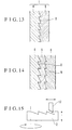
- Fig. 11 shows a case where a diffractive optical element 1 having one diffraction grating 4 formed on a base plate 2 is formed on a certain surface in an optical system.
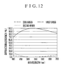
- the diffraction efficiency for diffraction light of a specific order of diffraction is obtained as shown in Fig. 12, which shows in a graph the characteristic of the diffraction efficiency.
- the abscissa axis of the graph indicates wavelength and the ordinate axis indicates diffraction efficiency.
- the diffractive optical element 1 is designed to have the highest diffraction efficiency at the first order of diffraction (shown in a full line curve in Fig. 12) in the useful wavelength region.
- the design diffraction order of this diffractive optical element is the first order.
- the graph of Fig. 12 also shows the diffraction efficiency of diffraction light obtained at diffraction orders near the design order, i.e., a zero order and a second order (1 + 1).
- the diffraction efficiency at the design order becomes highest at a certain wavelength (540 nm) (hereinafter referred to as the design wavelength) and gradually lowers at other wavelengths.
- the design wavelength a certain wavelength (540 nm)
- Such a lowering portion of the diffraction efficiency obtained at the design order becomes diffraction light of other orders, thereby appearing as flare light.
- a drop in diffraction efficiency at wavelengths other than the design wavelength eventually causes a decrease in transmission factor.
- document JP-A-9-127321 An arrangement of lessening such a drop in diffraction efficiency is disclosed in document JP-A-9-127321 and document JP-A-9-127322.
- the diffractive optical element disclosed in document JP-A-9-127321 is in a sectional shape formed by laminating two layers 4 and 5, as shown in Fig. 13.
- the diffractive optical element disclosed in document JP-A-9-127322 is of such a grating structure that three layers 4, 5 and 6 are laminated as shown in Fig. 14. As shown in Fig. 14, the layer 5, which is sandwiched between two diffraction grating surfaces 8 and 9 provided at the boundaries of the layers 4, 5 and 6, has a thickness which varies with portions thereof. In this diffractive optical element, each of the diffraction grating surfaces 8 and 9 is formed between two different materials. A high diffraction efficiency is attained by optimizing a difference in refractive power between the layer materials located in front and in rear of the boundary and the grating thicknesses of the diffraction grating surfaces. Moreover, the diffractive optical element disclosed in document JP-A-9-127322 is designed to be a thin-type diffractive optical element such that the diffraction efficiency has a relatively low wavelength dependency and a low dependency on the angle of incidence.
- diffractive optical element disclosed in document JP-A-9-127322 and the diffractive optical element according to the invention have those features in common which are recited in the preamble of claim 1.
- the diffractive optical elements necessitate a wavelength characteristic of the difference in refractive power between the materials in front and in rear of each of grating areas to have desired values, it is impossible to have a larger difference in refractive power than in a case where a grating area has air on one side thereof instead of a layer material.
- their gratings must be arranged to have a relatively large grating thickness.
- the grating thickness is 10 ⁇ m or thereabout.
- the number of layers of different materials is increased to three and the number of grating surfaces is increased to two.
- One of the two gratings measures at least 6 ⁇ m in thickness, so that a considerably deep grating shape would be recognized.
- the above-stated grating shapes can be formed by cutting.
- a product thus obtained by cutting either may be used directly as a diffractive optical element or may be used as a mold for duplicating diffractive optical elements.
- the grating thickness is large as mentioned above, the amount of cutting by the cutting process increases to cause the cutting tool edge to be greatly abraded.
- the shape of the tool edge obtained at the commencement of cutting differs from its shape obtained at the end of cutting.
- Such abrasion causes the grating thickness at its point where the cutting comes to an end to become thinner than a desired value.
- the grating shape comes to deviate from a desired saw-tooth like shape.
- the slanting plane of grating slants steeper than the one-layer type conventional diffractive optical element. Therefore, the fore end of the cutting tool edge must be formed at a sharper angle than the slanting plane of grating. This necessitates use of a cutting tool edge at a sharper angle than a cutting tool edge for the one-layer type conventional diffractive optical element. The sharper angle of the cutting tool edge then causes the cutting tool edge to be more readily abraded.
- the abrasion of the cutting tool edge may be abated by arranging its fore end part to have a duller angle.
- the duller tool edge angle necessitates the slanting plane of the saw-tooth-shaped (or serrated) grating to have a duller angle for preventing it from interfering with the cutting tool edge.
- the adoption of the laminated structure causes the grating thickness to be thicker and to have steeper slanting plane than the grating of an ordinary one-layer type diffractive optical element.
- an attempt to moderate the angle of the slanting plane of the laminated structure causes a great increase in grating pitch.
- the usable range of such a diffractive optical element therefore, would be limited by the increase in grating pitch.
- optical systems of varied kinds such as a photo-taking optical system and an observation optical system, can be arranged to include the diffractive optical element defined in the claims.
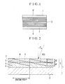
- Fig. 1 is a front view of a diffractive optical element according to a first embodiment of the invention.
- the diffractive optical element 1 shown in Fig. 1 includes a base plate 2 and a lamination part (diffraction grating part) 3 which is formed on the surface of the base plate 2 and which is composed of a plurality of layers (diffraction gratings) 4, 5, 6 and 7 shown in Fig. 2.
- Fig. 2 is a sectional view of the diffractive optical element 1 taken along a line A-A' shown in Fig. 1.
- the diffractive optical element 1 is shown in an exaggerated shape in the direction of depth of the diffraction grating part 3.
- the diffractive optical element 1 is formed by laminating, on the base plate 2, a total of four layers, i.e., the first layer 4, the second layer 5, the third layer 6 and the fourth layer 7.
- a first diffraction grating surface 8 is formed between the first layer 4 and the second layer 5.
- a second diffraction grating surface 9 is formed between the third layer 6 and the fourth layer 7.
- a boundary part between the second layer 5 and the third layer 6 is formed to be a flat part having no grating.
- the first layer 4 and the third layer 6 are made of the same material.
- the second layer 5 and the fourth layer 7 are made of the same material. Then, all the layers 4, 5, 6 and 7 are combined to act as one diffractive optical element 1.
- each layer (4, 5, 6 or 7) which has a diffraction grating surface formed on one side and periodically changes the thickness of its layer material in a cycle of a length P (hereinafter referred to as the grating pitch) is called a diffraction grating.
- Each of the diffraction gratings in the first embodiment is arranged to be a blazed-type diffraction grating, which is obtained by approximating the so-called kinoform with a triangular wave.
- grating thickness d of the diffraction grating a difference in height between the crest and trough of the diffraction grating surface is herein called the grating thickness d of the diffraction grating.
- the diffractive optical element is arranged to be in a grating structure in which at least three diffraction gratings, i.e., at least two diffraction grating surfaces, made of at least two materials which differ from each other in dispersion (Abbe number ⁇ d) are laminated on the base plate 2, to have a high diffraction efficiency at a specific (design) diffraction order within a useful wavelength region (visible spectrum), and to make the grating thickness d of each diffraction grating so small as compared with the grating pitch P thereof, that the following condition is satisfied: d/P ⁇ 1/6 . Further, with numerical values concretely presented, the following condition is satisfied: 1 ⁇ m ⁇ d ⁇ 6 ⁇ m.
- the diffraction efficiency of the diffractive optical element according to the first embodiment of the invention is next described as follows.
- a difference d0 in optical path length (hereinafter referred to as the optical path length difference of a diffraction grating surface), must be integer times as much as the design wavelength ⁇ 0, when a light flux is made perpendicularly incident on the diffractive optical element.
- n01 represents the refractive index of the material of the layer 4 for the design wavelength ⁇ 0
- n02 represents the refractive index of the material of the other layer 5 for the design wavelength ⁇ 0
- d represents the grating thickness of the diffraction grating 4 or 5
- m represents a design order of diffraction.
- the diffractive optical element corresponds to the diffractive optical element 1 shown in Fig. 11 composed of one layer.
- the diffractive optical element In order to have all the layers act as one diffraction grating, the diffractive optical element must be configured such that a sum value obtained by adding together all values of optical path length difference between the crest and trough of diffraction grating surfaces formed at boundaries between the layers becomes integer times as much as the design wavelength. Therefore, in the case of the first embodiment shown in Fig.
- a diffractive optical element of the conventional laminated two-layer structure In the case of a diffractive optical element of the conventional laminated two-layer structure, machining work on the diffractive optical element is difficult as it is difficult to obtain a sufficient difference in refractive index between materials forming a boundary.
- a diffractive optical element of the invention on the other hand, a diffractive optical element is divided into a plurality of diffraction gratings of thin grating thicknesses which can be easily machined, and the thus-obtained diffraction gratings are laminated.
- a conventional two-layer structure shown in Fig. 13 is first described by way of example as follows.
- the grating thickness of the first diffraction grating 4 is 11.9 ⁇ m.
- a minimum pitch necessary for the lens is assumed, for example, to be 40 ⁇ m.
- the angle of the slanting plane of the diffraction grating surface becomes 16.6° at the minimum pitch. If the diffraction grating is to be formed by the above-stated cutting process, the edge angle of the cutting tool edge must be arranged to be not exceeding 73.4°.
- the arrangement according to the invention is next described as follows.
- the grating structure of the diffractive optical element is assumed to be as shown in Fig. 2.
- the same materials mentioned above are assumed to be used for forming the diffraction gratings.
- the grating thickness d1 of the first (second) diffraction grating and the grating thickness d2 of the third (fourth) diffraction grating are both 5.95 ⁇ m.
- the grating thicknesses d1 and d2 may be of any values as long as a sum of them becomes the above-stated value of 11.9 ⁇ m. However, they are preferably arranged to be equal to each other, because such arrangement permits use of one mold in common for both of them in the case of forming the diffraction gratings by molding and one tool edge in common for both of them if the diffraction gratings are to be formed by cutting, instead of molding.
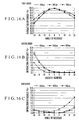
- Fig. 3 shows the diffraction efficiency of the structure of the first embodiment obtained for the useful wavelength region.
- the first embodiment has a high diffraction efficiency at the design order of diffraction in the same manner as the conventional arrangement.
- the edge angle of the cutting tool edge can be arranged to be not exceeding 81.5°.
- the edge angle of the cutting tool edge can be duller than in the case of the conventional arrangement. Further, since the grating thickness of each diffraction grating is only half of that of the conventional arrangement, the amount of cutting the diffraction grating surface is only half of that of the conventional arrangement. By virtue of these two advantageous points, the abrasion of the cutting tool edge is reduced to a great extent, so that the diffractive optical element can be easily manufactured to have uniform grating thickness over the whole area thereof.
- the edge angle of the cutting tool edge is preferably a dull angle measuring at least 80°.
- the grating thickness of the diffraction grating assumed to be "d” and the minimum grating pitch of the diffraction grating assumed to be "P” the grating thickness of each of the diffraction gratings is determined to satisfy the condition of d/P ⁇ 1/6. It is also possible to lessen the abrasion of the cutting tool edge by combining thin diffraction gratings which measure only 6 ⁇ m or less in grating thickness to lessen the cutting amount.
- the diffractive optical element of the invention gives a better workability by diving the diffraction grating into two. Further, in a case where a combination of materials causes a further increase in grating thickness, the improved workability can be retained by dividing the diffractive optical element not only into three but into a greater number of parts such as four parts and then by laminating these divided diffraction gratings.
- the diffraction grating shape has been described by limiting it to a shape obtained within one period of diffraction grating.
- the diffraction efficiency is basically not affected by the pitch of diffraction grating.
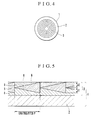
- the above-stated arrangement of the first embodiment is applicable not only to the one-dimensional diffractive optical element shown in Fig. 1 but also to diffractive optical elements of any different grating shapes, such as a diffractive lens shown in Fig. 4.
- the first embodiment described above is a diffractive optical element having diffraction gratings arranged on a flat plate.
- the same advantageous effect can be attained by arranging the diffraction gratings on a curved lens surface.
- the first embodiment has been described for a case where the design diffraction order is the first order. It is, however, not limited to the first order. With a design diffraction order arranged to be other than the first order, such as the second order, the same advantageous effect is attainable by setting a composite optical path length difference to become a desired design wavelength at the desired diffraction order. Further, one and the same material may be used both for the base plate 2 and the first diffraction grating 4.
- Figs. 7A, 7B and 7C show the incident-angle dependency of the diffraction efficiency in a case where the first embodiment is arranged to have a grating pitch P at 59.5 ⁇ m with the grating thicknesses d1 and d2 set at 5.95 ⁇ m. As apparent from Fig.
- the diffraction efficiency in respect of the incident-angle dependency of the diffraction efficiency for the second-order diffraction light, the diffraction efficiency has large values at incident angles of ⁇ ⁇ -15° and above for wavelengths 550 nm and 450 nm. Therefore, for general use, the diffraction efficiency is restricted by incident angles (a parasitic diffraction light component is to be suppressed within 3%) . In this instance, the value of d/P is 1/10.
- This causes a conspicuous flare light component, which is hardly desirable for image forming performance.
- the value of d/P is 1/5.
- the value of d/P is 1/20 in each of these cases.
- a diffractive optical element of the laminated structure having diffraction gratings slanting in the same direction in a grating sectional shape is arranged to have the value of d/P less than 1/6.
- Fig. 5 is a sectional view showing essential parts of a diffractive optical element according to a second embodiment of the invention.
- the two divided diffraction grating surfaces are arranged to have the same slant direction.
- at least one of a plurality of gratings is arranged to have a grating surface with a slant direction which differs from the slant direction of the grating surfaces of the other diffraction gratings.
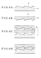
- the diffractive optical element according to the second embodiment of the invention is composed of three layers, i.e., a first layer 4, a second layer 5 and a third layer 6, as shown in Fig. 5.
- the grating (or slant) direction of the first diffraction grating surface 8 differs from that of the second diffraction grating surface 9.
- the diffraction efficiency of the second embodiment is the same as that of the first embodiment for a perpendicular incident light flux, as the materials with the diffraction grating surface 9 at a boundary thereof are arranged reversely to those of the first embodiment.
- the arrangement of the second embodiment is characterized by the thinness of the gratings, so that the workability of the diffractive optical element can be greatly improved.
- a diffraction grating having a flat datum plane as shown in Fig. 5 if the absolute values of the grating thicknesses d1 and d2 of the first and third diffraction gratings 4 and 6 are equal to each other, the grating shape of the first layer 4 and that of the third layer 6 are identical with each other. Therefore, the diffractive optical element according to the second embodiment can be manufactured by a manufacturing method as shown in Figs. 6A to 6D.
- the grating part of the first layer 4 and that of the third layer 6 can be formed by molding with one and the same mold, as shown in Figs. 6A and 6B. Then, the material of the second layer 5 is filled into a space between the two grating parts, as shown in Fig. 6C, so that the diffractive optical element 1 is formed as shown in Fig. 6D.
- that of the second embodiment curtails manufacturing processes as it has a less number of layers by one than the first embodiment.
- a diffractive optical element In cases where a diffractive optical element is used as a part of an image forming optical system, the optical system is rarely arranged to have only a light flux perpendicularly incident on the diffractive optical element.
- the diffractive optical element is, therefore, used for a range of specific incident angles in general.
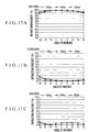
- Figs. 7A, 7B and 7C show the relationship between the diffraction efficiency and the incident angle in the first embodiment.
- Figs. 8A, 8B and 8C show the relationship between the diffraction efficiency and the incident angle in the second embodiment.
- Figs. 7A and 8A show the variations of the diffraction efficiency in relation to the incident angle of diffraction light of the first order
- Figs. 7B and 8B show the variations of the diffraction efficiency in relation to the incident angle of diffraction light of the second order
- Figs. 7C and 8C show the variations of the diffraction efficiency in relation to the incident angle of diffraction light of the zero order.
- the incident light flux is within a plane defined by the grating pitch direction of the diffraction grating and the normal line of the diffraction grating surface.
- the diffraction light flux is assumed to be within one plane.
- the sign of incident angle the direction of ⁇ shown in Fig. 2 is assumed to indicate positive values.
- the total of the grating thicknesses is 8 ⁇ m
- the grating pitch is 40 ⁇ m.
- the variations of the diffraction efficiency at negative (-) incident angles in the grating structure of the second embodiment are suppressed to a greater degree than in the grating structure of the first embodiment.
- the incident angle 6 in order to suppress the diffraction efficiency for diffraction orders other than the design order to 3% or less, the incident angle 6 must be within a range of -15° ⁇ ⁇ ⁇ 20° in the case of the first embodiment, whereas the second embodiment allows the incident angle 6 to have a wider range of -20° ⁇ ⁇ ⁇ 20°.
- the width of light flux and the grating pitch of the diffractive lens have variously values. Therefore, a usable range of angles of view and an allowable diffraction efficiency for the design diffraction order must be decided in combination most apposite to every case.
- an advantage of the grating structure of the second embodiment lies in that the variations of the diffraction efficiency for variations in incident angle can be suppressed.
- Another advantage of the second embodiment lies in that, in a case where the shape of a datum plane is a flat surface, the manufacturing processes for the diffractive optical element can be shortened.
- Fig. 9 is a sectional view schematically showing an optical system having the diffractive optical element of the invention according to a third embodiment thereof.
- the optical system is an image forming optical system of a camera or the like.
- a photo-taking lens 10 includes therein a diaphragm 11 and the diffractive optical element 1.
- An image forming plane 12 represents a film or a CCD.
- the wavelength dependency of the diffraction efficiency of the third embodiment is greatly improved by the use of the diffractive optical element 1 which is of the laminated structure. Therefore, the photo-taking lens does not have much flare, has a high resolution at low frequencies and thus has a high performance. Since the diffractive optical element can be simply formed in accordance with the invention, the photo-taking lens can be manufactured by mass production at low cost.
- the diffractive optical element 1 is disposed on the flat glass surface near the diaphragm 11.
- the disposition of the diffractive optical element is not limited to such position and may be on the curved surface of a lens. Further, a plurality of diffractive optical elements may be disposed within the photo-taking lens.
- the invention is applied to the photo-taking lens of a camera in the case of the third embodiment, the invention is not limited to it.
- the same advantages can be attained by applying the invention to a photo-taking lens of a video camera, an image scanner of a business machine, a reader lens of a digital copying machine, etc.
- Fig. 10 is a sectional view schematically showing an optical system having the diffractive optical element of the invention according to a fourth embodiment thereof.
- the optical system is an observation optical system of a binocular or the like.
- the optical system shown in Fig. 10 includes an objective lens 13, an image inverting prism 14 for erecting an image, an eyepiece lens 15, and an evaluation plane (pupil plane) 16.
- reference numeral 1 denotes the diffractive optical element, which is used for the purpose of correcting chromatic aberration of the objective lens 13 appearing on an image forming plane 12.
- the wavelength dependency of the diffraction efficiency of the fourth embodiment is greatly improved by the use of the diffractive optical element 1 of the laminated structure.
- the objective lens therefore, does not have much flare, has a high resolution at low frequencies and thus has a high performance.
- the diffractive optical element according to the invention can be simply formed, the observation optical system can be manufactured by mass production at low cost.
- the diffractive optical element 1 is formed at the objective lens 13.
- the same advantageous effects can be attained with the diffractive optical element 1 disposed either on the surface of the prism 14 or within the eyepiece lens 15. Since the effect of abating chromatic aberration can be attained solely through the objective lens 13 with the diffractive optical element 1 disposed on the object side of the image forming plane 12, the diffractive optical element 1 is preferably disposed at least on the side of the objective lens 13 in the case of an observation optical system.
- the invention is applied to a binocular.
- the arrangement of the fourth embodiment applies not only to it but also to a terrestrial telescope, an astronomical telescope or the like.
- the same advantages are also attainable by applying the arrangement to an optical viewfinder of a lens-shutter type camera, a video camera or the like.
Landscapes
- Physics & Mathematics (AREA)
- General Physics & Mathematics (AREA)
- Optics & Photonics (AREA)
- Geometry (AREA)
- Diffracting Gratings Or Hologram Optical Elements (AREA)
- Lenses (AREA)
Applications Claiming Priority (3)
| Application Number | Priority Date | Filing Date | Title |
|---|---|---|---|
| JP262833/97 | 1997-09-10 | ||
| JP26283397A JP3472103B2 (ja) | 1997-09-10 | 1997-09-10 | 回折光学素子及びそれを用いた光学系 |
| JP26283397 | 1997-09-10 |
Publications (3)
| Publication Number | Publication Date |
|---|---|
| EP0902304A2 EP0902304A2 (en) | 1999-03-17 |
| EP0902304A3 EP0902304A3 (en) | 1999-04-07 |
| EP0902304B1 true EP0902304B1 (en) | 2005-08-03 |
Family
ID=17381255
Family Applications (1)
| Application Number | Title | Priority Date | Filing Date |
|---|---|---|---|
| EP98116857A Expired - Lifetime EP0902304B1 (en) | 1997-09-10 | 1998-09-07 | Diffractive optical element and optical system having the same |
Country Status (4)
| Country | Link |
|---|---|
| US (1) | US6624943B2 (enExample) |
| EP (1) | EP0902304B1 (enExample) |
| JP (1) | JP3472103B2 (enExample) |
| DE (1) | DE69831041T2 (enExample) |
Families Citing this family (57)
| Publication number | Priority date | Publication date | Assignee | Title |
|---|---|---|---|---|
| JP3530776B2 (ja) | 1999-07-28 | 2004-05-24 | キヤノン株式会社 | 回折光学素子及びそれを用いた光学系 |
| US6831783B2 (en) | 2000-06-07 | 2004-12-14 | Canon Kabushiki Kaisha | Diffractive optical element and optical system |
| JP4587418B2 (ja) * | 2000-09-27 | 2010-11-24 | キヤノン株式会社 | 回折光学素子及び該回折光学素子を有する光学系 |
| JP3733294B2 (ja) | 2001-02-19 | 2006-01-11 | キヤノン株式会社 | 走査光学装置及びそれを用いた画像形成装置 |
| US20030161044A1 (en) * | 2002-02-04 | 2003-08-28 | Nikon Corporation | Diffractive optical element and method for manufacturing same |
| DE60324062D1 (de) | 2002-06-17 | 2008-11-27 | Canon Kk | Optisches Beugungselement und damit ausgestattetes optisches System |
| WO2004025335A1 (de) | 2002-08-24 | 2004-03-25 | Carl Zeiss Smt Ag | Binär geblazetes diffraktives optisches element |
| DE10322239B4 (de) | 2003-05-17 | 2011-06-30 | Carl Zeiss SMT GmbH, 73447 | Geblazetes diffraktives optisches Element sowie Projektionsobjektiv mit einem solchen Element |
| DE10322238B4 (de) | 2003-05-17 | 2007-10-31 | Carl Zeiss Smt Ag | Diffraktives optisches Element sowie Projektionsobjektiv mit einem solchen Element |
| US20080007831A1 (en) | 2004-09-29 | 2008-01-10 | Seiji Nishiwaki | Optical Element |
| US7756660B2 (en) * | 2004-12-28 | 2010-07-13 | Asml Netherlands B.V. | Lithographic apparatus and device manufacturing method |
| DE102005036633A1 (de) * | 2005-08-04 | 2007-06-21 | Carl Zeiss Ag | Achromatisches diffraktives optisches Element sowie Verfahren zum Entwerfen eines solchen |
| TWI413795B (zh) * | 2006-09-15 | 2013-11-01 | 尼康股份有限公司 | 攝影透鏡以及照相機 |
| US11726332B2 (en) | 2009-04-27 | 2023-08-15 | Digilens Inc. | Diffractive projection apparatus |
| JP2011022255A (ja) * | 2009-07-14 | 2011-02-03 | Canon Inc | 回折光学素子及びそれを有する光学系 |
| US11300795B1 (en) | 2009-09-30 | 2022-04-12 | Digilens Inc. | Systems for and methods of using fold gratings coordinated with output couplers for dual axis expansion |
| US11320571B2 (en) * | 2012-11-16 | 2022-05-03 | Rockwell Collins, Inc. | Transparent waveguide display providing upper and lower fields of view with uniform light extraction |
| US10795160B1 (en) | 2014-09-25 | 2020-10-06 | Rockwell Collins, Inc. | Systems for and methods of using fold gratings for dual axis expansion |
| JP5546217B2 (ja) * | 2009-11-20 | 2014-07-09 | キヤノン株式会社 | 回折光学素子およびそれを有する光学系、撮像装置 |
| JP2012083382A (ja) * | 2010-10-06 | 2012-04-26 | Canon Inc | 回折光学素子、光学系および光学機器 |
| WO2012136970A1 (en) | 2011-04-07 | 2012-10-11 | Milan Momcilo Popovich | Laser despeckler based on angular diversity |
| WO2016020630A2 (en) | 2014-08-08 | 2016-02-11 | Milan Momcilo Popovich | Waveguide laser illuminator incorporating a despeckler |
| US8634139B1 (en) | 2011-09-30 | 2014-01-21 | Rockwell Collins, Inc. | System for and method of catadioptric collimation in a compact head up display (HUD) |
| JP5342665B2 (ja) * | 2012-03-12 | 2013-11-13 | ファナック株式会社 | 渦巻き状計測経路に沿って計測を行うレンズ形状加工方法およびレンズ形状加工装置 |
| EP2842003B1 (en) | 2012-04-25 | 2019-02-27 | Rockwell Collins, Inc. | Holographic wide angle display |
| US9933684B2 (en) | 2012-11-16 | 2018-04-03 | Rockwell Collins, Inc. | Transparent waveguide display providing upper and lower fields of view having a specific light output aperture configuration |
| US10088675B1 (en) | 2015-05-18 | 2018-10-02 | Rockwell Collins, Inc. | Turning light pipe for a pupil expansion system and method |
| WO2016113534A1 (en) | 2015-01-12 | 2016-07-21 | Milan Momcilo Popovich | Environmentally isolated waveguide display |
| US9632226B2 (en) | 2015-02-12 | 2017-04-25 | Digilens Inc. | Waveguide grating device |
| US11366316B2 (en) | 2015-05-18 | 2022-06-21 | Rockwell Collins, Inc. | Head up display (HUD) using a light pipe |
| US10126552B2 (en) | 2015-05-18 | 2018-11-13 | Rockwell Collins, Inc. | Micro collimator system and method for a head up display (HUD) |
| US9910276B2 (en) | 2015-06-30 | 2018-03-06 | Microsoft Technology Licensing, Llc | Diffractive optical elements with graded edges |
| US10670862B2 (en) | 2015-07-02 | 2020-06-02 | Microsoft Technology Licensing, Llc | Diffractive optical elements with asymmetric profiles |
| US10038840B2 (en) | 2015-07-30 | 2018-07-31 | Microsoft Technology Licensing, Llc | Diffractive optical element using crossed grating for pupil expansion |
| US9864208B2 (en) * | 2015-07-30 | 2018-01-09 | Microsoft Technology Licensing, Llc | Diffractive optical elements with varying direction for depth modulation |
| US10073278B2 (en) | 2015-08-27 | 2018-09-11 | Microsoft Technology Licensing, Llc | Diffractive optical element using polarization rotation grating for in-coupling |
| EP3359999A1 (en) | 2015-10-05 | 2018-08-15 | Popovich, Milan Momcilo | Waveguide display |
| US10429645B2 (en) | 2015-10-07 | 2019-10-01 | Microsoft Technology Licensing, Llc | Diffractive optical element with integrated in-coupling, exit pupil expansion, and out-coupling |
| US10241332B2 (en) | 2015-10-08 | 2019-03-26 | Microsoft Technology Licensing, Llc | Reducing stray light transmission in near eye display using resonant grating filter |
| US9946072B2 (en) * | 2015-10-29 | 2018-04-17 | Microsoft Technology Licensing, Llc | Diffractive optical element with uncoupled grating structures |
| US10234686B2 (en) | 2015-11-16 | 2019-03-19 | Microsoft Technology Licensing, Llc | Rainbow removal in near-eye display using polarization-sensitive grating |
| US11513350B2 (en) | 2016-12-02 | 2022-11-29 | Digilens Inc. | Waveguide device with uniform output illumination |
| WO2018129398A1 (en) | 2017-01-05 | 2018-07-12 | Digilens, Inc. | Wearable heads up displays |
| US10108014B2 (en) * | 2017-01-10 | 2018-10-23 | Microsoft Technology Licensing, Llc | Waveguide display with multiple focal depths |
| US10295824B2 (en) | 2017-01-26 | 2019-05-21 | Rockwell Collins, Inc. | Head up display with an angled light pipe |
| KR102768598B1 (ko) | 2018-01-08 | 2025-02-13 | 디지렌즈 인코포레이티드. | 도파관 셀 내의 홀로그래픽 격자의 높은 처리능력의 레코딩을 위한 시스템 및 방법 |
| WO2019136473A1 (en) | 2018-01-08 | 2019-07-11 | Digilens, Inc. | Methods for fabricating optical waveguides |
| WO2020149956A1 (en) | 2019-01-14 | 2020-07-23 | Digilens Inc. | Holographic waveguide display with light control layer |
| TWI831898B (zh) * | 2019-01-15 | 2024-02-11 | 德商卡爾蔡司Smt有限公司 | 藉由破壞性干涉抑制至少一目標波長的光學繞射元件 |
| WO2020163524A1 (en) | 2019-02-05 | 2020-08-13 | Digilens Inc. | Methods for compensating for optical surface nonuniformity |
| US20220283377A1 (en) | 2019-02-15 | 2022-09-08 | Digilens Inc. | Wide Angle Waveguide Display |
| EP3924759B1 (en) | 2019-02-15 | 2025-07-30 | Digilens Inc. | Methods and apparatuses for providing a holographic waveguide display using integrated gratings |
| CN114207492A (zh) | 2019-06-07 | 2022-03-18 | 迪吉伦斯公司 | 带透射光栅和反射光栅的波导及其生产方法 |
| KR102775783B1 (ko) | 2019-08-29 | 2025-02-28 | 디지렌즈 인코포레이티드. | 진공 격자 및 이의 제조 방법 |
| US12066592B2 (en) * | 2020-02-28 | 2024-08-20 | Samsung Electronics Co., Ltd. | Meta-optical device and electronic apparatus including the same |
| WO2022150841A1 (en) | 2021-01-07 | 2022-07-14 | Digilens Inc. | Grating structures for color waveguides |
| JP2024508926A (ja) | 2021-03-05 | 2024-02-28 | ディジレンズ インコーポレイテッド | 真空周期的構造体および製造の方法 |
Citations (4)
| Publication number | Priority date | Publication date | Assignee | Title |
|---|---|---|---|---|
| US5581405A (en) * | 1993-12-29 | 1996-12-03 | Eastman Kodak Company | Hybrid refractive/diffractive achromatic camera lens and camera using such |
| JPH09127322A (ja) * | 1995-08-29 | 1997-05-16 | Olympus Optical Co Ltd | 回折光学素子 |
| US5631779A (en) * | 1993-05-24 | 1997-05-20 | Olympus Optical Co., Ltd. | Objective lens system |
| US6157488A (en) * | 1995-08-29 | 2000-12-05 | Olympus Optical Company Ltd. | Diffractive optical element |
Family Cites Families (12)
| Publication number | Priority date | Publication date | Assignee | Title |
|---|---|---|---|---|
| US4245882A (en) * | 1977-11-04 | 1981-01-20 | Environmental Research Institute Of Michigan | Doubly modulated on-axis thick hologram optical element |
| US5048925A (en) | 1985-05-28 | 1991-09-17 | Advanced Environmental Research Group | Quasi volume diffracting structures |
| US5044706A (en) | 1990-02-06 | 1991-09-03 | Hughes Aircraft Company | Optical element employing aspherical and binary grating optical surfaces |
| JPH06324262A (ja) | 1993-05-11 | 1994-11-25 | Olympus Optical Co Ltd | 撮像光学系 |
| US5589983A (en) | 1993-12-29 | 1996-12-31 | Eastman Kodak Company | Method of manufacturing a diffractive surface profile |
| US5606434A (en) * | 1994-06-30 | 1997-02-25 | University Of North Carolina | Achromatic optical system including diffractive optical element |
| US5446588A (en) * | 1994-07-29 | 1995-08-29 | The University Of Rochester | Wide-angle eyepiece optical system employing refractive and diffractive optical elements |
| US5847877A (en) * | 1994-09-12 | 1998-12-08 | Olympus Optical Co., Ltd. | Diffractive optical element |
| JP3717555B2 (ja) | 1994-09-12 | 2005-11-16 | オリンパス株式会社 | 回折光学素子 |
| JP3407477B2 (ja) * | 1995-06-08 | 2003-05-19 | 松下電器産業株式会社 | 位相格子とその作製方法並びに光学式エンコーダ |
| JP3472092B2 (ja) | 1997-07-28 | 2003-12-02 | キヤノン株式会社 | 回折光学素子及びそれを用いた光学系 |
| JP3472097B2 (ja) | 1997-08-20 | 2003-12-02 | キヤノン株式会社 | 回折光学素子及びそれを用いた光学系 |
-
1997
- 1997-09-10 JP JP26283397A patent/JP3472103B2/ja not_active Expired - Fee Related
-
1998
- 1998-09-07 EP EP98116857A patent/EP0902304B1/en not_active Expired - Lifetime
- 1998-09-07 DE DE69831041T patent/DE69831041T2/de not_active Expired - Lifetime
-
2001
- 2001-07-05 US US09/898,029 patent/US6624943B2/en not_active Expired - Lifetime
Patent Citations (4)
| Publication number | Priority date | Publication date | Assignee | Title |
|---|---|---|---|---|
| US5631779A (en) * | 1993-05-24 | 1997-05-20 | Olympus Optical Co., Ltd. | Objective lens system |
| US5581405A (en) * | 1993-12-29 | 1996-12-03 | Eastman Kodak Company | Hybrid refractive/diffractive achromatic camera lens and camera using such |
| JPH09127322A (ja) * | 1995-08-29 | 1997-05-16 | Olympus Optical Co Ltd | 回折光学素子 |
| US6157488A (en) * | 1995-08-29 | 2000-12-05 | Olympus Optical Company Ltd. | Diffractive optical element |
Also Published As
| Publication number | Publication date |
|---|---|
| EP0902304A2 (en) | 1999-03-17 |
| DE69831041D1 (de) | 2005-09-08 |
| EP0902304A3 (en) | 1999-04-07 |
| JP3472103B2 (ja) | 2003-12-02 |
| US6624943B2 (en) | 2003-09-23 |
| US20010036012A1 (en) | 2001-11-01 |
| JPH1184118A (ja) | 1999-03-26 |
| DE69831041T2 (de) | 2006-05-24 |
Similar Documents
| Publication | Publication Date | Title |
|---|---|---|
| EP0902304B1 (en) | Diffractive optical element and optical system having the same | |
| US6560019B2 (en) | Diffractive optical element and optical system having the same | |
| EP1072906B1 (en) | Diffraction optical element | |
| EP0898182B1 (en) | Diffractive optical element and optical system having the same | |
| EP0895100B1 (en) | Method of designing a diffractive optical element | |
| US6873463B2 (en) | Diffractive optical element and optical system having the same | |
| US6587272B2 (en) | Diffractive optical element | |
| US6650477B2 (en) | Diffractive optical element and optical apparatus having the same | |
| EP0895099B1 (en) | Diffractive optical element and optical system having the same | |
| EP1239305A1 (en) | Achromatic diffractive optical element with a plurality of layers | |
| JP4227210B2 (ja) | 回折光学素子及びそれを用いた光学系 | |
| US20020196545A1 (en) | Diffractive optical element and photographic optical system having the same | |
| EP1376161B1 (en) | Diffractive optical element and optical system provided with the same | |
| EP1186914B1 (en) | Diffractive optical element and optical system having the same |
Legal Events
| Date | Code | Title | Description |
|---|---|---|---|
| PUAI | Public reference made under article 153(3) epc to a published international application that has entered the european phase |
Free format text: ORIGINAL CODE: 0009012 |
|
| PUAL | Search report despatched |
Free format text: ORIGINAL CODE: 0009013 |
|
| AK | Designated contracting states |
Kind code of ref document: A2 Designated state(s): DE FR GB IT NL |
|
| AX | Request for extension of the european patent |
Free format text: AL;LT;LV;MK;RO;SI |
|
| AK | Designated contracting states |
Kind code of ref document: A3 Designated state(s): AT BE CH CY DE DK ES FI FR GB GR IE IT LI LU MC NL PT SE |
|
| AX | Request for extension of the european patent |
Free format text: AL;LT;LV;MK;RO;SI |
|
| 17P | Request for examination filed |
Effective date: 19990831 |
|
| AKX | Designation fees paid |
Free format text: DE FR GB IT NL |
|
| 17Q | First examination report despatched |
Effective date: 20000324 |
|
| GRAP | Despatch of communication of intention to grant a patent |
Free format text: ORIGINAL CODE: EPIDOSNIGR1 |
|
| GRAS | Grant fee paid |
Free format text: ORIGINAL CODE: EPIDOSNIGR3 |
|
| GRAA | (expected) grant |
Free format text: ORIGINAL CODE: 0009210 |
|
| AK | Designated contracting states |
Kind code of ref document: B1 Designated state(s): DE FR GB IT NL |
|
| PG25 | Lapsed in a contracting state [announced via postgrant information from national office to epo] |
Ref country code: NL Free format text: LAPSE BECAUSE OF FAILURE TO SUBMIT A TRANSLATION OF THE DESCRIPTION OR TO PAY THE FEE WITHIN THE PRESCRIBED TIME-LIMIT Effective date: 20050803 |
|
| REG | Reference to a national code |
Ref country code: GB Ref legal event code: FG4D |
|
| REF | Corresponds to: |
Ref document number: 69831041 Country of ref document: DE Date of ref document: 20050908 Kind code of ref document: P |
|
| NLV1 | Nl: lapsed or annulled due to failure to fulfill the requirements of art. 29p and 29m of the patents act | ||
| ET | Fr: translation filed | ||
| PLBE | No opposition filed within time limit |
Free format text: ORIGINAL CODE: 0009261 |
|
| STAA | Information on the status of an ep patent application or granted ep patent |
Free format text: STATUS: NO OPPOSITION FILED WITHIN TIME LIMIT |
|
| 26N | No opposition filed |
Effective date: 20060504 |
|
| PGFP | Annual fee paid to national office [announced via postgrant information from national office to epo] |
Ref country code: DE Payment date: 20140930 Year of fee payment: 17 |
|
| PGFP | Annual fee paid to national office [announced via postgrant information from national office to epo] |
Ref country code: GB Payment date: 20140924 Year of fee payment: 17 |
|
| PGFP | Annual fee paid to national office [announced via postgrant information from national office to epo] |
Ref country code: IT Payment date: 20140903 Year of fee payment: 17 |
|
| PGFP | Annual fee paid to national office [announced via postgrant information from national office to epo] |
Ref country code: FR Payment date: 20140924 Year of fee payment: 17 |
|
| REG | Reference to a national code |
Ref country code: DE Ref legal event code: R119 Ref document number: 69831041 Country of ref document: DE |
|
| PG25 | Lapsed in a contracting state [announced via postgrant information from national office to epo] |
Ref country code: IT Free format text: LAPSE BECAUSE OF NON-PAYMENT OF DUE FEES Effective date: 20150907 |
|
| GBPC | Gb: european patent ceased through non-payment of renewal fee |
Effective date: 20150907 |
|
| REG | Reference to a national code |
Ref country code: FR Ref legal event code: ST Effective date: 20160531 |
|
| PG25 | Lapsed in a contracting state [announced via postgrant information from national office to epo] |
Ref country code: DE Free format text: LAPSE BECAUSE OF NON-PAYMENT OF DUE FEES Effective date: 20160401 Ref country code: GB Free format text: LAPSE BECAUSE OF NON-PAYMENT OF DUE FEES Effective date: 20150907 |
|
| PG25 | Lapsed in a contracting state [announced via postgrant information from national office to epo] |
Ref country code: FR Free format text: LAPSE BECAUSE OF NON-PAYMENT OF DUE FEES Effective date: 20150930 |