EP0901128A2 - Verfahren und Anordnung zur Justierung und Steuerung eines interaktiven Verfahrens zur Aufnahme von analogen Signalen durch On-Chip-Auswahl einer Spannungsrampenamplitude - Google Patents
Verfahren und Anordnung zur Justierung und Steuerung eines interaktiven Verfahrens zur Aufnahme von analogen Signalen durch On-Chip-Auswahl einer Spannungsrampenamplitude Download PDFInfo
- Publication number
- EP0901128A2 EP0901128A2 EP98307093A EP98307093A EP0901128A2 EP 0901128 A2 EP0901128 A2 EP 0901128A2 EP 98307093 A EP98307093 A EP 98307093A EP 98307093 A EP98307093 A EP 98307093A EP 0901128 A2 EP0901128 A2 EP 0901128A2
- Authority
- EP
- European Patent Office
- Prior art keywords
- voltage
- circuit
- programming
- ramp
- control circuit
- Prior art date
- Legal status (The legal status is an assumption and is not a legal conclusion. Google has not performed a legal analysis and makes no representation as to the accuracy of the status listed.)
- Withdrawn
Links
- 238000000034 method Methods 0.000 title claims abstract description 11
- 230000002452 interceptive effect Effects 0.000 title 1
- 230000015654 memory Effects 0.000 claims abstract description 26
- 230000009467 reduction Effects 0.000 claims abstract description 6
- 239000003990 capacitor Substances 0.000 claims description 27
- 238000004519 manufacturing process Methods 0.000 claims description 4
- 230000005540 biological transmission Effects 0.000 claims description 3
- 230000001808 coupling effect Effects 0.000 claims 3
- 238000007599 discharging Methods 0.000 claims 2
- 230000002708 enhancing effect Effects 0.000 claims 2
- 238000005259 measurement Methods 0.000 abstract description 2
- 230000008878 coupling Effects 0.000 description 6
- 238000010168 coupling process Methods 0.000 description 6
- 238000005859 coupling reaction Methods 0.000 description 6
- 230000003247 decreasing effect Effects 0.000 description 3
- 238000010586 diagram Methods 0.000 description 2
- 230000004044 response Effects 0.000 description 2
- 230000008859 change Effects 0.000 description 1
- 238000012804 iterative process Methods 0.000 description 1
Images


Classifications
-
- G—PHYSICS
- G11—INFORMATION STORAGE
- G11C—STATIC STORES
- G11C27/00—Electric analogue stores, e.g. for storing instantaneous values
- G11C27/005—Electric analogue stores, e.g. for storing instantaneous values with non-volatile charge storage, e.g. on floating gate or MNOS
-
- G—PHYSICS
- G11—INFORMATION STORAGE
- G11C—STATIC STORES
- G11C11/00—Digital stores characterised by the use of particular electric or magnetic storage elements; Storage elements therefor
- G11C11/56—Digital stores characterised by the use of particular electric or magnetic storage elements; Storage elements therefor using storage elements with more than two stable states represented by steps, e.g. of voltage, current, phase, frequency
- G11C11/5621—Digital stores characterised by the use of particular electric or magnetic storage elements; Storage elements therefor using storage elements with more than two stable states represented by steps, e.g. of voltage, current, phase, frequency using charge storage in a floating gate
-
- G—PHYSICS
- G11—INFORMATION STORAGE
- G11C—STATIC STORES
- G11C11/00—Digital stores characterised by the use of particular electric or magnetic storage elements; Storage elements therefor
- G11C11/56—Digital stores characterised by the use of particular electric or magnetic storage elements; Storage elements therefor using storage elements with more than two stable states represented by steps, e.g. of voltage, current, phase, frequency
- G11C11/5621—Digital stores characterised by the use of particular electric or magnetic storage elements; Storage elements therefor using storage elements with more than two stable states represented by steps, e.g. of voltage, current, phase, frequency using charge storage in a floating gate
- G11C11/5628—Programming or writing circuits; Data input circuits
-
- G—PHYSICS
- G11—INFORMATION STORAGE
- G11C—STATIC STORES
- G11C16/00—Erasable programmable read-only memories
- G11C16/02—Erasable programmable read-only memories electrically programmable
- G11C16/06—Auxiliary circuits, e.g. for writing into memory
- G11C16/30—Power supply circuits
-
- G—PHYSICS
- G11—INFORMATION STORAGE
- G11C—STATIC STORES
- G11C2211/00—Indexing scheme relating to digital stores characterized by the use of particular electric or magnetic storage elements; Storage elements therefor
- G11C2211/56—Indexing scheme relating to G11C11/56 and sub-groups for features not covered by these groups
- G11C2211/562—Multilevel memory programming aspects
- G11C2211/5621—Multilevel programming verification
-
- G—PHYSICS
- G11—INFORMATION STORAGE
- G11C—STATIC STORES
- G11C2211/00—Indexing scheme relating to digital stores characterized by the use of particular electric or magnetic storage elements; Storage elements therefor
- G11C2211/56—Indexing scheme relating to G11C11/56 and sub-groups for features not covered by these groups
- G11C2211/562—Multilevel memory programming aspects
- G11C2211/5624—Concurrent multilevel programming and programming verification
Definitions
- the present invention relates to the field of analog storage devices. More particularly, this invention relates to a circuit and method for adjusting the voltage applied to a gate of a non-volatile memory cell to improve programming accuracy.
- NV memory cells such as Electrically Erasable Programmable Read Only Memory (EEPROM) cells.
- EEPROM Electrically Erasable Programmable Read Only Memory
- Cell programming may be accomplished by applying programming voltage to a drain of a targeted EEPROM cell in accordance to a read-while-writing voltage program technique of U.S. Patent No. 5,629,890.
- U.S. Patent No. 5,629,890 describes the read-while-writing voltage program technique in which a voltage present on a source terminal of the EEPROM cell is provided to a comparator and compared with a selected target voltage.
- the selected target voltage is a slightly reduced voltage sampled from an input analog signal. So long as the selected target voltage is greater than the source voltage of the EEPROM cell, a high voltage ramp is supplied to the EEPROM cell. Once the selected target voltage has been reached, the supply of the high voltage ramp to the EEPROM cell is discontinued and a new voltage is calculated and loaded into the comparator to continue programming as needed.
- the "coupling ratio” is a ratio of (i) the capacitance between a floating gate and a drain terminal of the floating gate transistor and (ii) the capacitance between the floating gate and a control gate. While the read-while-write voltage program technique tolerates many electrical characteristic variations, it remains vulnerable to variations in the coupling ratio. Such vulnerability occurs when a predetermined, generally constant voltage is applied to the control gate.
- this new target voltage will be artificially large, not a small incremental voltage as intended.
- the programming of EEPROM cells is an iterative process, the source voltage measured during the read-while-write voltage program technique will become impractically large where the target voltage can be greater than the supply voltage provided by a power supply.
- the present invention relates to a circuit and method for adjusting ramp voltage applied to the gate of a non-volatile memory cell to improve programming accuracy caused by a voltage applied to the drain of the non-volatile memory. This can be accomplished by measuring an amount of additional voltage realized at a source of the floating gate transistor. Thereafter, a compensation ratio may be selected to reduce an amplitude of the ramp voltage applied to a control gate of the memory cell by an amount necessary to lessen the amount of additional voltage realized at the source of the floating gate transistor. This will reduce inaccurate measurement of voltages during the read-while-write voltage program technique.
- the term “HIGH” is defined herein as providing sufficient voltage to turn-on a transistor.
- the term “LOW” is defined as providing sufficient voltage to turn-off a transistor.
- “Impedance” is generally defined as a measure of either resistance, capacitance or inductance.
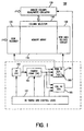
- the analog IC storage device 100 comprises a memory array 110 interconnected to a (i) row decoder 120, (ii) analog column read/write circuitry 130 and a column selector 140, and (iii) a row high voltage circuit 150.
- memory array 110 Central to the analog IC storage device 100, memory array 110 has "X" rows and “Y” columns of non-volatile (NV) memory cells, where "X" and "Y" are positive whole numbers.
- NV non-volatile
- memory array 110 includes a plurality of electrically erasable programmable read only memory (EEPROM) cells which are arranged in rows and columns and are accessed under any chosen addressing scheme such as page mode addressing.
- EEPROM electrically erasable programmable read only memory
- a high voltage generator circuit 160 generates and applies a ramp voltage to row decoder 120 and row high voltage circuit 150.
- High voltage generator circuit 160 includes high voltage timing and logic circuit 161 coupled to a high voltage oscillator 162, a charge pump 163, a row high voltage generator 164 and a column high voltage generator 165.
- the timing and logic circuit 161 provides timing signals used for programming and erasing purposes.
- High voltage oscillator 162 is coupled to charge pump 163, row high voltage generator 164 and to column high voltage generator 165 for clocking. More specific to the present invention, charge pump 163 applies a voltage to both row high voltage generator 164 and column high voltage generator 165.
- Row high voltage generator 164 includes a voltage control circuit 300 which controls a voltage ramp and amplitude (referred to as Clear Low Voltage "CLRLV”) provided to row high voltage circuit 150.
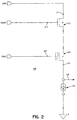
- CLRLV is applied to a control gate of a floating gate transistor of EEPROM cell shown in Figure 2.
- EEPROM cell 200 includes a first transistor 210 and a second 220 which is a floating gate transistor.
- a high voltage ramp (CHV2) is applied to a source 211 of transistor 210. Representing that the row of EEPROM cell 200 has been selected, a select signal is applied to gate 212.
- the select signal is set to a high voltage (e.g., greater than a maximum voltage of CHV2 by a threshold voltage drop).
- a "read-while-write" voltage line 230 is connected to a drain 221 of transistor 220 which is also connected to a current source 240.
- Voltage control circuit 300 includes an (operational) amplifier 310, a programmable feedback circuit 320, a reset circuit 330, a select circuit 340 and a plurality of programming circuits 350 and 360. Voltage control circuit 300 further includes (i) an output signal line 370 connected to an output 311 of amplifier 310 and (ii) a plurality of input signal lines 371-377.
- the output signal line 370 provides CLRLV to row high voltage circuit 150 of Figure 1, and in particular, to one or more control gates of corresponding EEPROM cell(s).
- the inputs corresponding to input signal lines 371-377 include a large swing logic signal (GATE4V), a high voltage ramp (CHV2), a reference voltage (INP), a bias voltage (VBP), a power down voltage (PD), and at least two trim bits (TR1 and TR2), respectively.
- GATE4V is applied to reset circuit 330 and select circuit 340 to initiate a reset condition for voltage control circuit 300 in response to a normal read operation.
- the reset and select circuits 330 and 340 are used to route CHV2 (a precise high voltage ramp) into an inverting input 312 of amplifier 310.
- INP is a constant voltage reference applied to a non-inverting input 313 of amplifier 310.
- VBP and PD are applied to inputs 314 and 315 of amplifier 310 in order to provide bias voltage to amplifier 310 and to signal amplifier 310 to reduce power consumption when idle.
- TR1 and TR2 are used to program the impedance of feedback circuit 320 of amplifier 310.
- This programmed impedance influences the voltage of CLRLV to follow one of four decreasing (negative) preset compensations having compensation ratios of 2:7, 2:9, 2:11 and 2:13.
- the "compensation ratio" is generally equivalent to a negative result of the voltage of CLRLV divided by the voltage of CHV2.
- this variation of compensation ratios is provided by placing more capacitors in parallel with each other.
- the capacitance values of capacitors of Figure 3 are shown in Table A. It is contemplated, however, that resistance could be used to provide the compensation ratios instead of or in combination with capacitance.
- the feedback circuit 320 would be slightly altered to support such impedance.
- Capacitor Picofarads Capacitor Picofarads C1 2 C58 2 C2 2 C59 2 C56 2 C82 2 C57 1 C83 2
- a voltage increase of CHV2 generally causes a voltage decrease of CLRLV. More specifically, when CHV2 is prevented from being applied to its inverting input 312, amplifier 310 produces a constant voltage for CLRLV. This constant voltage is equivalent to the selected voltage of INP (V inp ). Once CHV2 is applied to the inverting input 312 of amplifier 310, amplifier 310 produces a decreased voltage based on the feedback capacitance programmed by TR1 and TR2 as described below.
- GATE4V is set to a minimal voltage to turn-off transistor M4 of select circuit 340 and to turn-on transistor M79 of select circuit 340.
- CHV2 begins to increase at a first (positive) ramp rate 400 and to charge capacitor C1 of select circuit 340.
- the first ramp rate 400 is a design choice such as approximately 1V/ ⁇ s in this embodiment. Since CHV2 is currently incapable of turning on transistor M81 of select circuit 340, the voltage level of CLRLV 405 initially is maintained at the voltage of INP (V inp ). In this embodiment, the voltage of INP is equivalent to 3.5V.
- CHV2 turns-on transistor M81 of select circuit 340 to electrically connect select circuit 340 to node W03 (represented at time 410 of Figure 4)
- CHV2 is applied to inverting input 311 of amplifier 310.
- the voltage needed to turn-on transistor M81 is arbitrarily chosen as 3.5V.
- This causes a voltage reduction in CLRLV based on the capacitance of feedback circuit 320.
- the reduction is in accordance with a decreasing (negative) selectable preset compensation 420, 430, 440 and 450 shown as compensation ratios of 2:7, 2:9, 2:11 and 2:13, respectively.
- compensations are based on the particular selection of TR1 and TR2. It is contemplated, however, that more, less or different compensation ratios may be provided in lieu of or in addition to those illustrated.
- programming circuit 350 is used to place capacitors C58 and C83 in parallel with capacitors C1, C2, C57 and C59 while programming circuit 360 is used to place capacitor C56 in parallel with capacitors C1, C2, C57 and C59.
- an inverter formed by transistors M64 and M67 turns-on transmission gate (e.g., transistors M68 and M69). This causes the total capacitance provided by capacitor switching unit 320 to increase by the capacitive values associated with capacitors C58 and C83. Otherwise, if TR1 is LOW, transistors M68 and M69 are turned-off, disconnecting capacitors C58 and C83 from parallel capacitors C1, C2, C57 and C59.
- transistors M71 and M76 when TR2 is HIGH, an inverter formed by transistors M71 and M76 turns-on transistors M70 and M75. This causes the total capacitance provided by capacitor switching unit 320 to increase by the capacitive value associated with capacitor C56. Otherwise, if TR2 is LOW, transistors M70 and M75 are turned-off which disconnects capacitor C56 from parallel capacitors C1, C2, C57 and C59.
- GATE4V is set to a voltage sufficient to turn-on transistor M4. This causes capacitor C1 to be discharged.
- transistor M79 is turned-off and transistor M8 is turned-on in order to discharge all capacitors C1, C2, C57, C59 (and optionally C58, C83 and/or C56 if TR1 and/or TR2 bits are set) coupled between output line 370 and node W03.
- amplifier 310 operates as a voltage follower to hold CLRLV at INP (e.g., 3.5V) as required by the analog IC storage device 100 of Figure 1 for performing a normal read operation.
- an ideal voltage compensation 500 is provided to output (CLRLV) of voltage control circuit 300 of Figure 3.
- This voltage compensation 500 is chosen to negate any additional voltage provided to the source voltage of the EEPROM cell caused by capacitive coupling between the floating gate and drain terminal as described above. Due to capacitive coupling variations of NV memory cells, this would result in unsatisfactory programming accuracy when multiple write cycles are used. For example, a first write cycle 510 would complete programming exactly when the memory cell has been programmed with a selected voltage. For subsequent write cycles (e.g., second and third write cycles 520 and 530), an over programming condition would result because this technique does not account for successive approximation.
Landscapes
- Engineering & Computer Science (AREA)
- Computer Hardware Design (AREA)
- Read Only Memory (AREA)
- For Increasing The Reliability Of Semiconductor Memories (AREA)
- Continuous-Control Power Sources That Use Transistors (AREA)
Applications Claiming Priority (2)
| Application Number | Priority Date | Filing Date | Title |
|---|---|---|---|
| US08/924,397 US5877984A (en) | 1997-09-05 | 1997-09-05 | Method and apparatus for adjustment and control of an iterative method of recording analog signals with on chip selection of a voltage ramp amplitude |
| US924397 | 1997-09-05 |
Publications (2)
| Publication Number | Publication Date |
|---|---|
| EP0901128A2 true EP0901128A2 (de) | 1999-03-10 |
| EP0901128A3 EP0901128A3 (de) | 2000-04-26 |
Family
ID=25450175
Family Applications (1)
| Application Number | Title | Priority Date | Filing Date |
|---|---|---|---|
| EP98307093A Withdrawn EP0901128A3 (de) | 1997-09-05 | 1998-09-03 | Verfahren und Anordnung zur Justierung und Steuerung eines interaktiven Verfahrens zur Aufnahme von analogen Signalen durch On-Chip-Auswahl einer Spannungsrampenamplitude |
Country Status (3)
| Country | Link |
|---|---|
| US (1) | US5877984A (de) |
| EP (1) | EP0901128A3 (de) |
| JP (1) | JPH11161350A (de) |
Families Citing this family (10)
| Publication number | Priority date | Publication date | Assignee | Title |
|---|---|---|---|---|
| US6275417B1 (en) * | 1999-10-08 | 2001-08-14 | Aplus Flash Technology, Inc. | Multiple level flash memory |
| US6301151B1 (en) | 2000-08-09 | 2001-10-09 | Information Storage Devices, Inc. | Adaptive programming method and apparatus for flash memory analog storage |
| US6873550B2 (en) * | 2003-08-07 | 2005-03-29 | Micron Technology, Inc. | Method for programming and erasing an NROM cell |
| US7068539B2 (en) * | 2004-01-27 | 2006-06-27 | Sandisk Corporation | Charge packet metering for coarse/fine programming of non-volatile memory |
| US7599224B2 (en) * | 2007-07-03 | 2009-10-06 | Sandisk Corporation | Systems for coarse/fine program verification in non-volatile memory using different reference levels for improved sensing |
| US7508715B2 (en) * | 2007-07-03 | 2009-03-24 | Sandisk Corporation | Coarse/fine program verification in non-volatile memory using different reference levels for improved sensing |
| KR100968122B1 (ko) | 2008-06-30 | 2010-07-06 | 주성대학산학협력단 | 정전압 회로 |
| TWI424301B (zh) * | 2009-12-24 | 2014-01-21 | Richwave Technology Corp | 以序列延遲方式來任意調變輸出電壓之電壓調節器及相關電壓調節方法 |
| KR20120015725A (ko) | 2010-08-13 | 2012-02-22 | 삼성전자주식회사 | 전압 제어 방법 및 이를 이용한 메모리 장치 |
| US8368437B2 (en) * | 2011-03-02 | 2013-02-05 | Taiwan Semiconductor Manufacturing Company, Ltd. | Phase locked loop with charge pump |
Family Cites Families (14)
| Publication number | Priority date | Publication date | Assignee | Title |
|---|---|---|---|---|
| US4628487A (en) * | 1984-08-14 | 1986-12-09 | Texas Instruments Incorporated | Dual slope, feedback controlled, EEPROM programming |
| US4989170A (en) * | 1988-06-09 | 1991-01-29 | National Semiconductor Corporation | Hybrid stochastic gradient for convergence of adaptive filter |
| JPH0453096A (ja) * | 1990-06-19 | 1992-02-20 | Toshiba Corp | アナログ記憶装置 |
| US5241494A (en) * | 1990-09-26 | 1993-08-31 | Information Storage Devices | Integrated circuit system for analog signal recording and playback |
| US5220531A (en) * | 1991-01-02 | 1993-06-15 | Information Storage Devices, Inc. | Source follower storage cell and improved method and apparatus for iterative write for integrated circuit analog signal recording and playback |
| DE4311358C2 (de) * | 1992-04-07 | 1999-07-22 | Mitsubishi Electric Corp | Nicht-flüchtige Halbleiterspeichereinrichtung und Betriebsverfahren für eine nicht-flüchtige Halbleiterspeichereinrichtung und Verfahren zum Programmieren von Information in eine nicht-flüchtige Halbleiterspeichereinrichtung |
| US5363055A (en) * | 1993-03-15 | 1994-11-08 | General Electric Company | Photodiode preamplifier with programmable gain amplification |
| US5623436A (en) * | 1993-06-17 | 1997-04-22 | Information Storage Devices | Method and apparatus for adjustment and control of an iterative method of recording analog signals with on-chip trimming techniques |
| US5629890A (en) * | 1994-09-14 | 1997-05-13 | Information Storage Devices, Inc. | Integrated circuit system for analog signal storing and recovery incorporating read while writing voltage program method |
| US5668756A (en) * | 1994-12-26 | 1997-09-16 | Nippon Steel Corporation | Multi-value level type non-volatile semiconductor memory unit and method of rewriting the same |
| US5627784A (en) * | 1995-07-28 | 1997-05-06 | Micron Quantum Devices, Inc. | Memory system having non-volatile data storage structure for memory control parameters and method |
| KR0172831B1 (ko) * | 1995-09-18 | 1999-03-30 | 문정환 | 비휘발성 메모리를 프로그램하는 방법 |
| KR0174501B1 (ko) * | 1995-12-19 | 1999-04-15 | 김광호 | 아날로그 저장매체의 프로그래밍 장치 |
| EP0782149B1 (de) * | 1995-12-29 | 2003-05-28 | STMicroelectronics S.r.l. | Anordnung zum Erzeugen und Regeln einer Gate-Spannung in einem nichtflüchtigen Speicher |
-
1997
- 1997-09-05 US US08/924,397 patent/US5877984A/en not_active Expired - Fee Related
-
1998
- 1998-09-03 EP EP98307093A patent/EP0901128A3/de not_active Withdrawn
- 1998-09-07 JP JP10252324A patent/JPH11161350A/ja active Pending
Also Published As
| Publication number | Publication date |
|---|---|
| EP0901128A3 (de) | 2000-04-26 |
| US5877984A (en) | 1999-03-02 |
| JPH11161350A (ja) | 1999-06-18 |
Similar Documents
| Publication | Publication Date | Title |
|---|---|---|
| US5926409A (en) | Method and apparatus for an adaptive ramp amplitude controller in nonvolatile memory application | |
| US6281716B1 (en) | Potential detect circuit for detecting whether output potential of potential generation circuit has arrived at target potential or not | |
| KR100233387B1 (ko) | 기준전위발생장치 및 그것을 구비한 반도체메모리장치 | |
| KR100260603B1 (ko) | 기록시 판독 전압 프로그램 방법을 통합한 아날로그신호 기억 및 복구용 집적회로 시스템 | |
| US6301161B1 (en) | Programming flash memory analog storage using coarse-and-fine sequence | |
| US5969987A (en) | Non-volatile electrically alterable semiconductor memory for analog and digital storage | |
| US7164604B2 (en) | Nonvolatile semiconductor memory | |
| US5699295A (en) | Current detection circuit for reading a memory in integrated circuit form | |
| US20110022905A1 (en) | Test Circuit and Method for Multilevel Cell Flash Memory | |
| US20020031003A1 (en) | Ferroelectric memory device | |
| US9129682B2 (en) | Semiconductor memory device and method of operating the same | |
| US5877984A (en) | Method and apparatus for adjustment and control of an iterative method of recording analog signals with on chip selection of a voltage ramp amplitude | |
| EP0331113B1 (de) | Halbleiterspeichervorrichtung | |
| US6473338B2 (en) | Analog voltage supply circuit for a non-volatile memory | |
| EP0842514B1 (de) | Flash-speichersystem mit reduzierten störungen und verfahren dazu | |
| US6970382B2 (en) | System and method for controlling logical value and integrity of data in memory systems | |
| US20240063788A1 (en) | Apparatuses and methods for compensating for crosstalk noise at input receiver circuits | |
| US5812458A (en) | Electrically-erasable and programmable ROM with pulse-driven memory cells | |
| EP1054408B1 (de) | Halbleiterspeicheranordnung | |
| JP2002260395A (ja) | メモリセル、特にマルチレベル不揮発性メモリセルの動的読取り方法および回路 | |
| EP1324344B1 (de) | Leseverstärkerstruktur für nichtflüchtige Multibitspeicheranordnungen und dazugehöriges Leseverfahren | |
| US6178118B1 (en) | Electrically programmable semiconductor device with multi-level wordline voltages for programming multi-level threshold voltages | |
| US10861546B2 (en) | Semiconductor memory device capable of adjusting a wordline voltage for a write operation | |
| US7203103B2 (en) | Ferroelectric memory device and electronic apparatus | |
| US5388070A (en) | Storage arrangement and method for operating the arrangement |
Legal Events
| Date | Code | Title | Description |
|---|---|---|---|
| PUAI | Public reference made under article 153(3) epc to a published international application that has entered the european phase |
Free format text: ORIGINAL CODE: 0009012 |
|
| AK | Designated contracting states |
Kind code of ref document: A2 Designated state(s): DE FR GB IT NL |
|
| AX | Request for extension of the european patent |
Free format text: AL;LT;LV;MK;RO;SI |
|
| RIC1 | Information provided on ipc code assigned before grant |
Free format text: 6G 11C 11/56 A, 6G 11C 27/00 B, 6G 11C 16/06 B |
|
| PUAL | Search report despatched |
Free format text: ORIGINAL CODE: 0009013 |
|
| AK | Designated contracting states |
Kind code of ref document: A3 Designated state(s): AT BE CH CY DE DK ES FI FR GB GR IE IT LI LU MC NL PT SE |
|
| AX | Request for extension of the european patent |
Free format text: AL;LT;LV;MK;RO;SI |
|
| 17P | Request for examination filed |
Effective date: 20001013 |
|
| AKX | Designation fees paid |
Free format text: DE FR GB IT NL |
|
| STAA | Information on the status of an ep patent application or granted ep patent |
Free format text: STATUS: THE APPLICATION IS DEEMED TO BE WITHDRAWN |
|
| 18D | Application deemed to be withdrawn |
Effective date: 20030401 |