US10861546B2 - Semiconductor memory device capable of adjusting a wordline voltage for a write operation - Google Patents
Semiconductor memory device capable of adjusting a wordline voltage for a write operation Download PDFInfo
- Publication number
- US10861546B2 US10861546B2 US16/572,275 US201916572275A US10861546B2 US 10861546 B2 US10861546 B2 US 10861546B2 US 201916572275 A US201916572275 A US 201916572275A US 10861546 B2 US10861546 B2 US 10861546B2
- Authority
- US
- United States
- Prior art keywords
- code
- wordline
- control
- bitline
- memory device
- Prior art date
- Legal status (The legal status is an assumption and is not a legal conclusion. Google has not performed a legal analysis and makes no representation as to the accuracy of the status listed.)
- Active
Links
- 239000004065 semiconductor Substances 0.000 title claims abstract description 36
- 238000001514 detection method Methods 0.000 claims description 22
- 230000004044 response Effects 0.000 claims description 9
- 230000007423 decrease Effects 0.000 claims description 6
- 238000000034 method Methods 0.000 description 25
- 230000008569 process Effects 0.000 description 21
- 230000003071 parasitic effect Effects 0.000 description 9
- 230000004913 activation Effects 0.000 description 6
- 239000012782 phase change material Substances 0.000 description 4
- 230000008859 change Effects 0.000 description 3
- 230000003247 decreasing effect Effects 0.000 description 3
- 238000007599 discharging Methods 0.000 description 3
- 230000004048 modification Effects 0.000 description 2
- 238000012986 modification Methods 0.000 description 2
- 101100203174 Zea mays SGS3 gene Proteins 0.000 description 1
- 230000009286 beneficial effect Effects 0.000 description 1
- 239000013078 crystal Substances 0.000 description 1
- 230000002542 deteriorative effect Effects 0.000 description 1
- 230000000977 initiatory effect Effects 0.000 description 1
- 238000004519 manufacturing process Methods 0.000 description 1
- 239000000463 material Substances 0.000 description 1
- 230000000630 rising effect Effects 0.000 description 1
Images


Classifications
-
- G—PHYSICS
- G11—INFORMATION STORAGE
- G11C—STATIC STORES
- G11C13/00—Digital stores characterised by the use of storage elements not covered by groups G11C11/00, G11C23/00, or G11C25/00
- G11C13/0002—Digital stores characterised by the use of storage elements not covered by groups G11C11/00, G11C23/00, or G11C25/00 using resistive RAM [RRAM] elements
- G11C13/0021—Auxiliary circuits
- G11C13/0069—Writing or programming circuits or methods
-
- G—PHYSICS
- G11—INFORMATION STORAGE
- G11C—STATIC STORES
- G11C13/00—Digital stores characterised by the use of storage elements not covered by groups G11C11/00, G11C23/00, or G11C25/00
- G11C13/0002—Digital stores characterised by the use of storage elements not covered by groups G11C11/00, G11C23/00, or G11C25/00 using resistive RAM [RRAM] elements
- G11C13/0004—Digital stores characterised by the use of storage elements not covered by groups G11C11/00, G11C23/00, or G11C25/00 using resistive RAM [RRAM] elements comprising amorphous/crystalline phase transition cells
-
- G—PHYSICS
- G11—INFORMATION STORAGE
- G11C—STATIC STORES
- G11C13/00—Digital stores characterised by the use of storage elements not covered by groups G11C11/00, G11C23/00, or G11C25/00
- G11C13/0002—Digital stores characterised by the use of storage elements not covered by groups G11C11/00, G11C23/00, or G11C25/00 using resistive RAM [RRAM] elements
- G11C13/0021—Auxiliary circuits
- G11C13/0023—Address circuits or decoders
- G11C13/0026—Bit-line or column circuits
-
- G—PHYSICS
- G11—INFORMATION STORAGE
- G11C—STATIC STORES
- G11C13/00—Digital stores characterised by the use of storage elements not covered by groups G11C11/00, G11C23/00, or G11C25/00
- G11C13/0002—Digital stores characterised by the use of storage elements not covered by groups G11C11/00, G11C23/00, or G11C25/00 using resistive RAM [RRAM] elements
- G11C13/0021—Auxiliary circuits
- G11C13/0023—Address circuits or decoders
- G11C13/0028—Word-line or row circuits
-
- G—PHYSICS
- G11—INFORMATION STORAGE
- G11C—STATIC STORES
- G11C13/00—Digital stores characterised by the use of storage elements not covered by groups G11C11/00, G11C23/00, or G11C25/00
- G11C13/0002—Digital stores characterised by the use of storage elements not covered by groups G11C11/00, G11C23/00, or G11C25/00 using resistive RAM [RRAM] elements
- G11C13/0021—Auxiliary circuits
- G11C13/0038—Power supply circuits
Definitions
- Various embodiments may relate to a semiconductor memory device capable of adjusting a wordline voltage during a write operation, and more particularly, to a semiconductor memory device capable of adjusting a wordline voltage according to an address of a cell during a write operation.
- phase change memory (PCM) device which uses a material having resistance characteristics that vary depending on its crystal structure, is being developed.
- the resistance value of a cell in a crystalline state is smaller than the resistance value of the cell in an amorphous state.
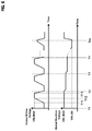
- FIG. 1 illustrates a read operation of a phase change memory device.
- the horizontal axis represents a voltage across a memory cell and the vertical axis represents a current (or a cell current) flowing through the memory cell that includes a phase change material.
- the read voltage V READ is a voltage across the memory cell.
- the cell current increases along lines (2) and (4) as the cell voltage increases, and thus remains lower than a threshold current I th when the cell voltage reaches the read voltage V READ .
- the cell current increases along lines (2) and (3) as the cell voltage increases, a snapback phenomenon (or snapback) occurs after reaching the threshold current I th , and then the cell current increase rapidly along line (1).
- the reciprocal of the slope of line (1) corresponds to the on resistance of the phase change material.
- the cell is programmed to a set state or a reset state in a write operation.
- a bitline driver supplies a current to a bitline coupled to the cell
- a wordline driver controls a voltage of the wordline coupled to the cell.
- a distance between the bitline driver and a specific cell and a distance between the wordline driver and the specific cell vary depending on a position of the cell in a memory cell array.
- parasitic resistance and parasitic capacitance associated with the cell also vary according to its position.
- a set threshold voltage and a reset threshold voltage of a cell may vary depending on its position.
- a semiconductor memory device may include a memory cell array including a plurality of wordlines, a plurality of bitlines and a plurality of cells; a bitline decoder configured to couple a global bitline to one of the plurality of bitlines according to a bitline selection signal; a bitline driver configured to provide bitline current to the global bitline; a wordline decoder configured to couple a global wordline to one of the plurality of wordlines according to a wordline selection signal; a wordline driver configured to provide a wordline drive voltage to the global wordline during a write operation and to adjust the wordline drive voltage according to a write address; and a write control circuit configured to generate the wordline selection signal and the bitline selection signal, and to control the bitline decoder, the wordline decoder, and the bitline driver.
- a memory device may include a first memory cell coupled to a first bitline and a first wordline; a second memory cell coupled to a second bitline and a second wordline; a wordline decoder configured to couple a global wordline to one of the first and second wordlines according to a wordline selection signal; a wordline driver configured to provide a wordline drive voltage to the global wordline during a write operation; and a code setting circuit configured to set a first control code corresponding to a first reference wordline drive voltage for the first memory cell, and to set a second control code corresponding to a second reference wordline drive voltage for the second memory cell.
- FIG. 1 illustrates a read operation of a semiconductor memory device.
- FIG. 2 illustrates a semiconductor memory device according to an embodiment of the present disclosure.
- FIG. 3 illustrates a bitline decoder and a wordline decoder according to an embodiment of the present disclosure.
- FIG. 4 illustrates a reference voltage generator according to an embodiment of the present disclosure.
- FIG. 5 illustrates a code setting circuit according to an embodiment of the present disclosure.
- FIG. 6 illustrates an operation of a code setting circuit to set a control code for a first cell according to an embodiment of the present disclosure.
- FIG. 7 illustrates an operation of a code setting circuit to set a control code for a second cell according to an embodiment of the present disclosure.
- FIG. 8 illustrates a data structure stored in a code setting circuit according to an embodiment of the present disclosure.
- FIG. 9 illustrates a memory cell array including a plurality of regions according to an embodiment of the present disclosure.
- FIG. 10 illustrates a data structure stored in a code setting circuit according to an embodiment of the present disclosure.
- FIG. 11A illustrates bitline voltages of a plurality of cells in a conventional memory device.
- FIG. 11B illustrates bitline voltages of a plurality of cells in a memory device according to an embodiment of the present disclosure.
- FIG. 2 illustrates a semiconductor memory device according to an embodiment of the present disclosure.
- a semiconductor memory device includes a memory cell array 1 , a wordline decoder 2 , a bitline decoder 3 , a bitline driver 4 , and a wordline driver 100 .
- a semiconductor memory device further includes a reference voltage generator 200 , a code setting circuit 300 , a snapback detector 400 , a code storage circuit 500 , a write control circuit 600 , and a command decoder 700 .
- the memory cell array 1 includes a plurality of memory cells.
- each of the plurality of memory cells may be referred to as a cell.
- FIG. 2 illustrates four cells C 1 , C 2 , C 3 , and C 4 as an example.
- a first cell C 1 represents a cell where a first wordline and a first bitline intersect
- a second cell C 2 represents a cell where the first wordline and a last bitline intersect.
- a third cell C 3 represents a cell where the last wordline and the first bitline intersect
- a fourth cell C 4 represents a cell where the last wordline and the last bitline intersect.
- the wordline decoder 2 provides a wordline drive voltage VWL to a selected wordline in accordance with a wordline selection signal WSEL.
- the bitline decoder 3 provides a bitline drive current IBL to a selected bitline in accordance with a bitline selection signal BSEL.
- the wordline selection signal WSEL and the bitline selection signal BSEL may be provided by the write control circuit 600 during a write operation.
- the code setting circuit 300 may provide the wordline selection signal WSEL and the bitline selection signal BSEL during a code setting operation.
- the bitline driver 4 provides the bitline drive current IBL to a global bitline GBL.
- the bitline driver 4 determines a waveform of the bitline drive current IBL according to an activation signal EN and a current control signal CCON.
- the activation signal EN and the current control signal CCON may be provided by the write control circuit 600 during a write operation.
- the code setting circuit 300 may provide the activation signal EN and the current control signal CCON during a code setting operation.
- the wordline driver 100 provides the wordline drive voltage VWL to the global wordline GWL.
- the wordline driver 100 generates the wordline drive voltage VWL based on a reference voltage VREF.
- the wordline driver 100 includes a first resistor 110 coupled between a power supply VDD and a first node N 1 , a second resistor 120 coupled between the first node N 1 and a second node N 2 , a transistor (e.g., an NMOS transistor) 130 whose source and drain are coupled between the second node N 2 and ground, and an operational amplifier 140 .
- a first resistor 110 coupled between a power supply VDD and a first node N 1
- a second resistor 120 coupled between the first node N 1 and a second node N 2
- a transistor 130 e.g., an NMOS transistor
- the operational amplifier 140 amplifies the voltage difference between the reference voltage VREF and a voltage at the first node N 1 and controls a gate voltage of the NMOS transistor 130 , thereby controlling the wordline drive voltage VWL output at the second node N 2 using a feedback operation.
- a negative feedback loop including the operation amplifier 140 with a negative gain, the transistor 130 , and the second resistor 120 operates to increase the wordline driver voltage VWL when the reference voltage VREF increases, and to decrease the wordline driver voltage VWL when the reference voltage VREF decreases.
- the operation amplifier 140 has a positive gain
- the operation amplifier 140 has a non-inverting input that is connected to the first node N 1 and an inverting input that receives the reference voltage VREF.
- the reference voltage generator 200 generates the reference voltage VREF based on a control code CCODE.
- FIG. 3 illustrates a memory cell array 1 , a wordline decoder 2 , and a bitline decoder 3 according to an embodiment of the present disclosure.
- the memory cell array 1 , the wordline decoder 2 , and the bitline decoder 3 in FIG. 3 may be suitable for use as the memory cell array 1 , the wordline decoder 2 , and the bitline decoder 3 in FIG. 2 , respectively.
- the memory cell array 1 includes a plurality of memory cells 11 and each memory cell 11 is coupled between a bitline BL and a wordline WL. Only a single memory cell 11 selected among the plurality of memory cells 11 is shown in FIG. 3 for the interest of brevity.
- the wordline decoder 2 includes a global wordline switch GN and a plurality of local wordline switches LN 1 to LNi.
- the wordline selection signal WSEL includes a global wordline switch control signal GX and a plurality of local wordline switch control signals LX 1 to LXi.
- the global wordline switch control signal GX controls the global wordline switch GN, and the plurality of local wordline switch control signals LX 1 to LXi control the plurality of local wordline switches LN 1 to LNi, respectively.
- the global wordline switch GN couples the global wordline GWL with a plurality of local wordlines LWL 1 to LWLi.
- the wordline decoder 2 further includes a wordline discharge switch DP for discharging the charge of the wordline WL in response to a wordline discharge control signal LXDISB.
- the bitline decoder 3 includes a global bitline switch GP and a plurality of local bitline switches LP 1 to LPj.
- the bitline selection signal BSEL includes a global bitline switch control signal GYB and a plurality of local bitline switch control signals LYB 1 to LYBj.
- the global bitline switch control signal GYB controls the global bitline switch GP, and the plurality of local bitline switch control signals LYB 1 to LYBj control the plurality of local bitline switches LP 1 to LPj, respectively.
- the global bitline switch GP connects the global bitline GBL with a plurality of local bitlines LBL 1 to LBLj.
- the bitline decoder 3 further includes a bitline discharge switch DN for discharging the charge of the bitline BL in response to a bitline discharge control signal LYDIS.
- FIG. 4 illustrates a reference voltage generator 200 according to an embodiment of the present disclosure.
- the reference voltage generator 200 in FIG. 4 may be suitable for use as the reference voltage generator 200 in FIG. 2 .
- the reference voltage generator 200 includes a plurality of resistors R 1 , R 1 to Rn, and R 02 , which are connected in series between a power supply VDD and ground.
- the reference voltage generator 200 further includes a plurality of switches SW 1 to SWn, each of which is controlled by a corresponding bit of a switch control code SCCODE.
- the switch control code SCCODE is obtained by performing a one-hot encoding operation on a control code (e.g., the control code CCODE in FIG. 2 ), and thus the switch control code SCCODE has a value with a single high bit and the remaining low bits.
- the first switch SW 1 is turned on while the remaining switches SW 2 to SWn are turned off when the switch control code SCCODE has a n-bit value of [0 0 . . . 0 1]
- the second switch SW 2 is turned on while the remaining switches SW 1 and SW 3 to SWn are turned off when the switch control code SCCODE has a n-bit value of [0 0 . . . 1 0], and so on.
- a first node of each of the plurality of switches SW 1 to SWn is commonly connected to an output node NO where the reference voltage VREF is output.
- a second node of each of the plurality of switches SW 1 to SWn is connected to a node between a corresponding pair of the plurality of resistors R 01 and R 1 to Rn.
- the second node of the first switch SW 1 is coupled to a node between the first resistor RO 1 and the second resistor R 1
- the second node of the second switch SW 2 is coupled to a node between the second resistor R 1 and the third resistor R 2 .
- the plurality of switches SW 1 to SWn are controlled according to the control code (e.g., the control code CCODE in FIG. 2 ), and accordingly, the reference voltage VREF is controlled to have a voltage which is obtained by dividing the supply voltage VDD with a corresponding resistance ratio.
- the first switch SW 1 is turned on to couple the node between the first resistor RO 1 and the second resistor R 1 to the output node NO when has the switch control code SSCODE has a n-bit value of [0 . . . 0 1].
- the second switch SW 2 is turned on to couple the node between the second resistor R 1 and the third resistor R 2 to the output node NO when has the switch control code SSCODE has a n-bit value of [0 . .
- a level of the reference voltage VREF decreases as the value of the switch control code SCCODE increases.
- the value of the switch control code SCCODE is a result of performing a one-hot encoding operation on the control code (e.g., the control code CCODE in FIG. 2 ), and thus the level of the reference voltage VREF decreases as the value of the control code increases.
- a level of the wordline drive voltage VWL varies according to an address of a cell during a write operation.
- the variance of set threshold voltages, or the variance of reset threshold voltages, or both may be reduced.
- the code setting circuit 300 sets the value of the control code CCODE used to generate the reference voltage VREF according to the address of the cell.
- Starting condition of a code setting operation by the code setting circuit 300 may vary according to the embodiment.
- the code setting circuit 300 may operate during an initialization process of a semiconductor memory device.
- the code setting circuit 300 may operate in response to an instruction by the command decoder 700 .
- a memory controller (not shown) may generate a command signal for initiating the code setting operation and provide the command signal to the semiconductor memory device.
- the code setting circuit 300 performs the code setting operation to determine the value of the control code CCODE according to a position of a cell and stores the control code CCODE in the code storage circuit 500 .
- the code setting circuit 300 controls the bitline driver 4 by generating an activation signal EN and a current control signal CCON during the code setting operation.
- the snapback detector 400 detects whether a snapback phenomenon has occurred in a cell (e.g., the memory cell 11 in FIG. 3 ) during the code setting operation.
- the snapback detector 400 may be implemented as a circuit generally used in the process of reading or writing a memory device, so that detailed descriptions will be omitted for the interest of brevity.
- the code storage circuit 500 stores the control code CCODE set by the code setting circuit 300 according to the address of the cell.
- the code storage circuit 500 may be implemented using a volatile memory device (e.g., a register, a DRAM), or a non-volatile memory device.
- a volatile memory device e.g., a register, a DRAM
- a non-volatile memory device e.g., a non-volatile memory device.
- the code setting circuit 300 performs a code setting operation during an initialization process of the semiconductor memory device.
- the code setting circuit 300 can further perform one or more code setting operations when the semiconductor memory device is used.
- the initial code setting operation may be performed during a production stage of the semiconductor memory device, or during an initialization process when the semiconductor memory device is used for the first time.
- the code setting circuit 300 and the snapback detector 400 may not be included in the semiconductor memory device but may be provided in a separate device.
- values of one or more control codes CCODE each can be predetermined and stored according to a corresponding cell address.
- the code storage circuit 500 is a volatile memory device, it may be preferable that the code setting circuit 300 and the snapback detector 400 are provided in the semiconductor memory device in order to perform a code setting operation when it is desirable.
- the write control circuit 600 performs one or more control operations during a write operation for a cell.
- the write control circuit 600 generates one or more signals to control the wordline decoder 2 , the bitline decoder 3 , and the bitline driver 4 during the write operation.
- the write control circuit 600 further refers to a write address and accesses the code storage circuit 500 to provide the reference voltage generator 200 with a control code CCODE corresponding to a selected cell based on the write address.
- the write control circuit 600 can adjust the wordline drive voltage VWL according to the write address during the write operation, and as a result, the variation (e.g., variance) of set threshold voltages, or the variation of reset threshold voltages, or both, can be reduced.
- variation e.g., variance
- the command decoder 700 receives a command signal and an address signal from a host like a memory controller.
- the command decoder 700 provides a write address to the write control circuit 600 in response to a write command and can control the write control circuit 600 to start a write operation.
- the command decoder 700 can control the code setting circuit 300 to perform the code setting operation during an initialization process of the semiconductor memory device.
- the code setting circuit 300 can be controlled using a signal (e.g., a power-on reset POR signal) indicating such an initialization process.
- the code setting circuit 300 can perform the code setting operation independently from the initialization process. For example, the code setting circuit 300 can perform the code setting operation without using the signal indicating the initialization process.
- the command decoder 700 may recognize a command for the code setting operation provided from the memory controller and may control the code setting circuit 300 to start the code setting operation in response to the command.
- FIG. 5 illustrates a code setting circuit 300 according to an embodiment of the present disclosure.
- the code setting circuit 300 includes a code changing circuit 310 and a setting control circuit 320 .
- the code changing circuit 310 changes a value of a control code CCODE according to a clock signal CLK and a snapback detection signal DET.
- the code changing circuit 310 includes a latch 311 , an inverter 3111 , an arithmetic circuit 312 , a register 313 , a first switch 314 , and a second switch 315 .
- the code changing circuit 310 uses an initial code INITC at the beginning of an operation of generating the control code CCODE and thereafter feeds back the control code CCODE.
- the first switch 314 is turned on to provide the initial code INITC as an input of the register 313 according to a first switch control signal LC.
- the second switch 315 is turned on in response to a second switch control signal (e.g., an inverted version of the first switch control signal/LC) to provide an output of the arithmetic circuit 312 as the input of the register 313 .
- a second switch control signal e.g., an inverted version of the first switch control signal/LC
- the latch 311 outputs a latch snapback detection signal DETD by latching the snapback detection signal DET according to the clock signal CLK.
- the inverter 3111 inverts the latch snapback detection signal DETD and outputs an inverted latch snapback detection signal /DETD.
- the latch 311 and the inverter 3111 may be referred as a step adjusting circuit and the inverted latch snapback detection signal/DETD may be referred as a step signal.
- the latch 311 may be connected after the inverter 3111 .
- the step signal/DETD has a value 0 or 1.
- the step signal/DETD may have a value 0 or k, where k is a positive number except 1.
- the arithmetic circuit 312 adds the step signal/DETD and an output of the latch 313 and outputs the addition result as the control code CCODE, and feeds the control code CCODE back to the register 313 .
- the register 313 latches the control code CCODE according to the clock signal CLK and provides an output thereof to the arithmetic circuit 312 .
- the initial code INITC is input to the adder 313 .
- the latch 311 When the snapback detection signal DET is at a first level (e.g., a logic low level) indicating that a snapback phenomenon is not detected, the latch 311 outputs a first value (e.g., 0), and the output value of the arithmetic circuit 312 becomes a value greater than the output value of the register 313 by 1.
- a first level e.g., a logic low level
- the latch 311 When the snapback detection signal DET is at a second level (e.g., a logic high level) indicating that a snapback phenomenon is detected, the latch 311 outputs a second value (e.g., 1) at the next rising edge of the clock signal CLK and the output value of the arithmetic circuit 312 after the next clock cycle keeps the output value of the register 313 at the current clock cycle.
- a second level e.g., a logic high level
- the setting control circuit 320 outputs the first switch control signal LC, an activation signal EN (e.g., the activation signal EN in FIG. 2 ), and a current control signal CCON (e.g., the current control signal CCON in FIG. 2 ) in response to the clock signal CLK and the snapback detection signal DET, and thereby controlling the code changing circuit 310 and a bitline driver (e.g., the bitline driver 4 in FIG. 2 ).
- an activation signal EN e.g., the activation signal EN in FIG. 2
- a current control signal CCON e.g., the current control signal CCON in FIG. 2
- the setting control circuit 320 further generates a wordline selection signal WSEL and a bitline selection signal BSEL corresponding to a target cell on which a code setting operation is performed, and outputs the wordline selection signal WSEL and the bitline selection signal BSEL to a wordline decoder (e.g., the wordline decoder 2 in FIG. 2 ) and a bitline decoder (e.g., the bitline decoder 3 in FIG. 2 ), respectively.
- a wordline decoder e.g., the wordline decoder 2 in FIG. 2
- a bitline decoder e.g., the bitline decoder 3 in FIG. 2
- the setting control circuit 320 provides the control code CCODE to a code storage circuit (e.g., the code storage circuit 500 in FIG. 2 ) when the snapback detection signal DET is asserted and finishes the code setting operation for the target cell according to the clock signal CLK.
- a code storage circuit e.g., the code storage circuit 500 in FIG. 2
- FIGS. 6 and 7 each illustrate a process of programming a cell to a reset state and determining a wordline drive voltage VWL to be applied to a cell, thereby making a reset threshold voltage of the cell substantially constant regardless of the position of the cell.
- the wordline drive voltage VWL represents a voltage of a global wordline (e.g, the global wordline GWL in FIGS. 2 and 3 ).
- FIG. 6 illustrates a process for setting a control code (e.g., the control code CCODE in FIG. 5 ) corresponding to the first cell C 1 of FIG. 2 according to an embodiment.
- a control code e.g., the control code CCODE in FIG. 5
- FIG. 7 illustrates a process for setting a control code corresponding to the second cell C 2 of FIG. 2 according to an embodiment.
- a bitline driver (e.g., the bitline driver 4 in FIG. 2 ) is deactivated at a first time T 1 and the voltage of the global wordline GWL (i.e., the word line drive voltage VWL) is set to the maximum value VWLMAX.
- bitline driver 4 is activated at a second time T 11 and a bitline current (e.g., the bitline current IBL in FIG. 2 ) is provided to a global bitline (e.g., the global bitline GBL in FIG. 2 ). Accordingly, when a snapback phenomenon does not occur, the global bitline voltage of the global bitline GBL rises to the maximum value VBLMAX at a third time T 12 .
- the maximum value VBLMAX of the global bitline voltage may correspond to the maximum value when a cell is programmed to the reset state.
- a snapback detector (e.g., the snapback detector 400 in FIG. 2 ) may detect whether the snapback phenomenon is occurred or not.
- bitline driver 4 is deactivated, and a wordline (e.g., the wordline WL in FIG. 3 ) and a bitline (e.g., the bitline BL in FIG. 3 ) coupled to the first cell C 1 are discharged to an initial state.
- a wordline e.g., the wordline WL in FIG. 3
- a bitline e.g., the bitline BL in FIG. 3
- the discharging process of the wordline and the bitline coupled to the first cell C 1 can be performed by controlling a wordline discharge switch (e.g., the wordline discharge switch DP in FIG. 3 ) and a bitline discharge switch (e.g., the bitline discharge switch DN in FIG. 3 ).
- a wordline discharge switch e.g., the wordline discharge switch DP in FIG. 3
- a bitline discharge switch e.g., the bitline discharge switch DN in FIG. 3
- the wordline drive voltage VWL is decreased by a given amount.
- Other processes in each of a control period from the fifth time T 2 to the sixth time T 3 and a control period from the sixth time T 3 to the seventh time T 4 are similar to those in a control period from the first time T 1 to the fifth time T 2 , and thus detailed descriptions thereof are omitted herein for the interest of brevity.
- the period of the clock signal CLK in FIG. 5 may be set to be longer than the control period (e.g., the control period from the first time T 1 to the fifth time T 2 ) described above.
- the value of the control code CCODE may be adjusted by a given value and the reference voltage VREF may be lowered by a given amount.
- the reference voltage VREF may be decreased by a predetermined value, thereby lowering the level of the reference voltage VREF by a predetermined amount.
- FIG. 6 shows that a snapback phenomenon is detected at an eighth time Tns during the the n-th control cycle (or n-th control period).
- the global bitline voltage does not rise to the maximum value VBLMAX, and then falls while the global wordline voltage (or the wordline drive voltage VWL) gradually rises from a snapback wordline voltage VWLSB.
- value of the control code CCODE at the (n+1)-th control cycle becomes as same as that at the n-th control cycle and the wordline drive voltage VWL used in the n-th control cycle is set as a first reference wordline drive voltage (e.g., a reference wordline drive voltage VWLREF in FIG. 7 ) for the first cell C 1 .
- a first reference wordline drive voltage e.g., a reference wordline drive voltage VWLREF in FIG. 7
- the first reference wordline drive voltage VWLREF is set to the wordline drive voltage VWL used in the n-th control cycle and the control code CCODE used in the n-th control cycle is stored in a code storage unit (e.g., the code storage circuit 500 in FIG. 2 ) to correspond to the address of the first cell C 1 .
- the wordline drive voltage VWL to be initially applied at a first time t 1 may be set to the first reference wordline drive voltage VWLREF of the first cell C 1 , thereby reducing the number of control cycles to determine the second reference wordline drive voltage of the second cell C 2 .
- the second cell C 2 is positioned farther away from a wordline driver (e.g., the wordline driver 100 in FIG. 2 ) than the first cell C 1 , parasitic resistance between a global wordline (e.g., the global wordline GWL in FIG. 2 ) and the second cell C 2 is greater than that between the global wordline and the first cell C 1 .
- a wordline driver e.g., the wordline driver 100 in FIG. 2
- parasitic resistance between a global wordline e.g., the global wordline GWL in FIG. 2
- the bitline driver 4 is deactivated and the global wordline voltage is set to the first reference wordline drive voltage VWLREF of the first cell C 1 .
- bitline driver 4 is activated at a second time t 11 and the bitline current IBL is provided to the global bitline GBL. Accordingly, when a snapback phenomenon does not occur, the global bitline voltage of the global bitline GBL rises to the maximum value VBLMAX at a third time t 12 .
- the snapback detector 400 may detect whether the snapback phenomenon is occurred or not.
- bitline driver 4 is deactivated, and the wordline and a bitline connected to the second cell C 2 are discharged to an initial state.
- the wordline drive voltage VWL is decreased by a given amount.
- Other processes in each of a control period from the fifth time t 2 to the sixth time t 3 and a control period from the sixth time t 3 to the seventh time t 4 are similar to those in a control period from the first time t 1 to the fifth time t 2 , and thus detailed descriptions thereof are omitted herein for the interest of brevity.
- the period of the clock signal CLK in FIG. 5 may be set to be longer than the control period (e.g., the control period from the first time t 1 to the fifth time t 2 ) described above.
- the reference voltage VREF can be lowered by a given level by adjusting the value of the control code CCODE by a given value.
- FIG. 7 shows that a snapback phenomenon is detected at an eight time tms during the m-th control cycle.
- the global bitline voltage does not rise to the maximum value VBLMAX, and then gradually falls while the wordline drive voltage VWL gradually rises from the snapback wordline voltage VWLSB 2 .
- the wordline drive voltage VWL used in the m-th cycle is set as the second reference wordline drive voltage of the second cell C 2 .
- the second reference wordline drive voltage of the second cell C 2 is set to the wordline drive voltage VWL used in the m-th control cycle, and the control code CCODE used in the m-th control cycle is stored in the code storage circuit 500 to correspond to the address of the second cell C 2 .
- Control codes CCODE for third and fourth cells C 3 and C 4 can be set using similar processes to the above-described processes with reference to FIGS. 6 and 7 .
- the first and third cells C 1 and C 3 are coupled to the first bitline.
- Other values of the control codes CCODE can be determined for any other cells coupled to the first bitline and disposed between the first and third cells C 1 and C 3 in light of the teachings and disclosures herein.
- control codes CCODE may be stored in the code storage circuit 500 to have a data structure as shown in FIG. 8 according to an embodiment.
- a write control circuit may access the code storage circuit 500 when a write address is input to determine a control code corresponding to a write address.
- a first code CODE 1 may be selected if a first write address corresponds to the first wordline and the first bitline coupled to the first cell C 1
- a second code CODE 2 may be selected if a second write address corresponds to the first wordline and the last bitline coupled to the second cell C 2 .
- the write control circuit 600 may generate a third control code corresponding to the third write address by applying an interpolation technique.
- the write control circuit 600 may obtain each of one or more intermediate values by interpolating a value of the first control code CODE 1 and a value of the second control code CODE 2 , thereby generating the third control code corresponding to the third write address.
- control code is determined using a linear interpolation method.
- embodiments of the present application are not limited thereto, and a different interpolation method may be used in another embodiment.
- FIG. 8 shows a case where the code storage circuit 500 stores the control codes CODE 1 to CODE 4 for four cells C 1 to C 4 .
- the first and second cells C 1 and C 2 are connected to the first wordline, and the third and fourth cells C 3 and C 4 are connected to the last wordline.
- the code storage circuit 500 stores a greater number of control codes respectively corresponding to a plurality of cells that are connected to a larger number of wordlines, a value of a control code that is not included in the table of FIG. 8 can be more accurately calculated using a specific interpolation method.
- FIG. 9 illustrates a memory cell array (e.g., the memory cell array 1 in FIG. 1 ) divided into a plurality of regions A 1 , A 2 , A 3 , and A 4 and determining a control code for a representative cell in each of the plurality of regions A 1 , A 2 , A 3 , and A 4 , according to an embodiment.
- a control code may be commonly used for cells in a corresponding region A 1 , A 2 , A 3 , or A 4 .
- the memory cell array 1 is divided into four regions A 1 , A 2 , A 3 , and A 4 , and cells located in the middle of the regions A 1 , A 2 , A 3 , and A 4 are denoted by C 1 , C 2 , C 3 , and C 4 , respectively.
- a process of determining a reference wordline drive voltage and a control code corresponding to each of the cells C 1 , C 2 , C 3 , and C 4 is substantially the same as that described with reference to FIGS. 6 and 7 , and thus detailed descriptions thereof are omitted in the interest of brevity.
- Control codes CODE 1 , CODE 2 , CODE 3 , and CODE 4 obtained for the cells C 1 , C 2 , C 3 , and C 4 in FIG. 9 may be stored in association with the regions A 1 , A 2 , A 3 , and A 4 , respectively, as shown in the table of FIG. 10 , according to an embodiment.
- the first control code CODE 1 corresponds to the first region A 1
- the second control code CODE 2 corresponds to the second area A 2
- the third control code CODE 3 corresponds to the third area A 3
- the fourth control code CODE 4 corresponds to the fourth area A 4 .
- Each of these control codes CODE 1 , CODE 2 , CODE 3 , and CODE 4 may be a control code for the entire cells in a corresponding region A 1 , A 2 , A 3 , or A 4 .
- the write control circuit 600 determines a region A 1 , A 2 , A 3 , or A 4 including a cell that corresponds to a write address, and can determine a control code CODE 1 , CODE 2 , CODE 3 , or CODE 4 corresponding to the determined region A 1 , A 2 , A 3 , or A 4 using the table of FIG. 10 .
- the write control circuit 660 may determine the control code CODE 1 , CODE 2 , CODE 3 , or CODE 4 corresponding to the write address.
- the number of regions may vary according to embodiments. As the number of regions increases, a fewer number of cells are set to have a common control code, and thus the variance of threshold voltages of a plurality of cells according to respective cell positions can be further reduced.
- a cell is programmed to a reset state such that the reset threshold voltage thereof is kept substantially constant regardless of parasitic resistance and parasitic capacitance associated with a position of the cell in a memory array.
- the variance of reset threshold voltages of a plurality of cells in the memory array according to an embodiment of the present disclosure may be reduced compared to that of a conventional memory array.
- the parasitic resistance and parasitic capacitance associated with the position of the cell also affects programming the cell to a set state.
- the cell is programmed to the set state such that the set threshold voltage may be kept substantially constant regardless of the parasitic resistance and parasitic capacitance associated with the position of the cell.
- the variance of set threshold voltages of a plurality of cells in a memory array according to an embodiment of the present disclosure may be reduced compared to that of the conventional memory array.
- a difference between the set threshold voltage and the reset threshold voltage of each of the plurality of cells is kept substantially constant, thereby improving the margin of a read voltage during a read operation, thereby reducing an occurrence of data error.
- a process of determining a control code so as to keep a reset threshold voltage of a cell substantially constant when the cell is programmed into a reset state has been disclosed.
- FIG. 11A illustrates bitline voltages of a plurality of cells in a conventional memory device.
- FIG. 11B illustrates bitline voltages of a plurality of cells in a memory device according to an embodiment of the present disclosure.
- FIG. 11A shows that a first voltage difference V 1 of the bitline voltages after the occurrence of the snapback phenomenon during a write operation, which depend on positions of a plurality of cells, is relatively large in the conventional memory device.
- FIG. 11B shows that a second voltage difference V 2 of the bitline voltages after the occurrence of the snapback phenomenon in a write operation according an embodiment of the present disclosure is reduced compared to that of the conventional memory device.
- Embodiments of the present disclosure adjusts a wordline drive voltage according to a position of each of a plurality cells in a memory array to reduce variance of threshold voltages of the plurality of cells. As a result, the variance of the bitline voltages of the plurality of cells after the occurrence of the snapback phenomenon decreases as shown in FIG. 11B .
Abstract
Description
Claims (20)
Applications Claiming Priority (4)
| Application Number | Priority Date | Filing Date | Title |
|---|---|---|---|
| KR20180162760 | 2018-12-17 | ||
| KR10-2018-0162760 | 2018-12-17 | ||
| KR1020190098561A KR20200074837A (en) | 2018-12-17 | 2019-08-13 | Semiconductor memory device capable of adjusting a word line voltage for a write operation |
| KR10-2019-0098561 | 2019-08-13 |
Publications (2)
| Publication Number | Publication Date |
|---|---|
| US20200194067A1 US20200194067A1 (en) | 2020-06-18 |
| US10861546B2 true US10861546B2 (en) | 2020-12-08 |
Family
ID=71072826
Family Applications (1)
| Application Number | Title | Priority Date | Filing Date |
|---|---|---|---|
| US16/572,275 Active US10861546B2 (en) | 2018-12-17 | 2019-09-16 | Semiconductor memory device capable of adjusting a wordline voltage for a write operation |
Country Status (1)
| Country | Link |
|---|---|
| US (1) | US10861546B2 (en) |
Families Citing this family (2)
| Publication number | Priority date | Publication date | Assignee | Title |
|---|---|---|---|---|
| KR20200141887A (en) * | 2019-06-11 | 2020-12-21 | 에스케이하이닉스 주식회사 | Semiconductor memory device including a control circuit for controlling a read operation |
| CN112740137A (en) * | 2020-12-23 | 2021-04-30 | 长江存储科技有限责任公司 | Voltage regulation for multiple voltage levels |
Citations (8)
| Publication number | Priority date | Publication date | Assignee | Title |
|---|---|---|---|---|
| US7307268B2 (en) * | 2005-01-19 | 2007-12-11 | Sandisk Corporation | Structure and method for biasing phase change memory array for reliable writing |
| US20110019495A1 (en) * | 2006-07-31 | 2011-01-27 | Scheuerlein Roy E | Decoder circuitry providing forward and reverse modes of memory array operation and method for biasing same |
| US20120044733A1 (en) * | 2010-08-20 | 2012-02-23 | Sandisk 3D Llc | Single Device Driver Circuit to Control Three-Dimensional Memory Element Array |
| KR101116407B1 (en) | 2009-03-12 | 2012-03-08 | 가부시끼가이샤 도시바 | Semiconductor memory device |
| US20140098594A1 (en) * | 2011-12-02 | 2014-04-10 | Panasonic Corporation | Cross point variable resistance nonvolatile memory device |
| US20150348626A1 (en) * | 2013-02-19 | 2015-12-03 | Panasonic Intellectual Property Management Co., Ltd. | Nonvolatile semiconductor storage device |
| US9299430B1 (en) * | 2015-01-22 | 2016-03-29 | Nantero Inc. | Methods for reading and programming 1-R resistive change element arrays |
| US20170032838A1 (en) * | 2015-07-31 | 2017-02-02 | Samsung Electronics Co., Ltd. | Resistive memory device |
-
2019
- 2019-09-16 US US16/572,275 patent/US10861546B2/en active Active
Patent Citations (10)
| Publication number | Priority date | Publication date | Assignee | Title |
|---|---|---|---|---|
| US7307268B2 (en) * | 2005-01-19 | 2007-12-11 | Sandisk Corporation | Structure and method for biasing phase change memory array for reliable writing |
| US20110019495A1 (en) * | 2006-07-31 | 2011-01-27 | Scheuerlein Roy E | Decoder circuitry providing forward and reverse modes of memory array operation and method for biasing same |
| KR101116407B1 (en) | 2009-03-12 | 2012-03-08 | 가부시끼가이샤 도시바 | Semiconductor memory device |
| US20120155149A1 (en) * | 2009-03-12 | 2012-06-21 | Kabushiki Kaisha Toshiba | Semiconductor storage device |
| US20120044733A1 (en) * | 2010-08-20 | 2012-02-23 | Sandisk 3D Llc | Single Device Driver Circuit to Control Three-Dimensional Memory Element Array |
| US20140098594A1 (en) * | 2011-12-02 | 2014-04-10 | Panasonic Corporation | Cross point variable resistance nonvolatile memory device |
| US20150348626A1 (en) * | 2013-02-19 | 2015-12-03 | Panasonic Intellectual Property Management Co., Ltd. | Nonvolatile semiconductor storage device |
| US9299430B1 (en) * | 2015-01-22 | 2016-03-29 | Nantero Inc. | Methods for reading and programming 1-R resistive change element arrays |
| US20170032838A1 (en) * | 2015-07-31 | 2017-02-02 | Samsung Electronics Co., Ltd. | Resistive memory device |
| KR20170014872A (en) | 2015-07-31 | 2017-02-08 | 삼성전자주식회사 | Resistive Memory Device |
Also Published As
| Publication number | Publication date |
|---|---|
| US20200194067A1 (en) | 2020-06-18 |
Similar Documents
| Publication | Publication Date | Title |
|---|---|---|
| US10410686B2 (en) | Memory modules storing a trimming control code associated with a minimum level of a power supply voltage, methods of operating the memory modules, and test systems of the memory modules | |
| US7391644B2 (en) | Phase-changeable memory device and read method thereof | |
| KR100745601B1 (en) | Phase change memory device and read method thereof | |
| US9939831B2 (en) | Fast settling low dropout voltage regulator | |
| JP2010182353A (en) | Semiconductor memory device and reading method therefor | |
| JP2002093153A (en) | Ferroelectric memory | |
| US7668007B2 (en) | Memory system including a resistance variable memory device | |
| JP3993354B2 (en) | Voltage generation circuit | |
| US8289778B2 (en) | Data processing device and method of reading trimming data | |
| JP2007087512A (en) | Nonvolatile semiconductor memory device and method for operating same | |
| US8228711B2 (en) | Bi-directional resistive memory devices and related memory systems and methods of writing data | |
| US20030133328A1 (en) | Current sense amplifier with dynamic pre-charge | |
| US10861546B2 (en) | Semiconductor memory device capable of adjusting a wordline voltage for a write operation | |
| JP2003242795A (en) | Nonvolatile semiconductor memory device and its power- up read method | |
| JP2013054800A (en) | Semiconductor device and method of manufacturing semiconductor device | |
| JP2003331591A (en) | Semiconductor memory device | |
| US20040196093A1 (en) | Fast, accurate and low power supply voltage booster using a/d converter | |
| US11443806B2 (en) | Nonvolatile memory and method of operating nonvolatile memory | |
| KR20200074837A (en) | Semiconductor memory device capable of adjusting a word line voltage for a write operation | |
| US9330794B1 (en) | DRAM-based anti-fuse cells | |
| CN112116943A (en) | Non-volatile memory device for mitigating read disturb and system using the same | |
| US7120041B2 (en) | Memory device with programmable parameter controller | |
| CN108615541B (en) | Bit line pre-charging and discharging circuit and memory | |
| US7839706B2 (en) | Dual mode accessing signal control apparatus and dual mode timing signal generating apparatus | |
| JP4593707B2 (en) | Memory cell sense amplifier |
Legal Events
| Date | Code | Title | Description |
|---|---|---|---|
| AS | Assignment |
Owner name: SK HYNIX INC., KOREA, REPUBLIC OF Free format text: ASSIGNMENT OF ASSIGNORS INTEREST;ASSIGNORS:PARK, HYUNKYU;KIM, SUHWAN;JEONG, DEOG-KYOON;REEL/FRAME:050392/0930 Effective date: 20190722 Owner name: SEOUL NATIONAL UNIVERSITY R&DB FOUNDATION, KOREA, REPUBLIC OF Free format text: ASSIGNMENT OF ASSIGNORS INTEREST;ASSIGNORS:PARK, HYUNKYU;KIM, SUHWAN;JEONG, DEOG-KYOON;REEL/FRAME:050392/0930 Effective date: 20190722 |
|
| FEPP | Fee payment procedure |
Free format text: ENTITY STATUS SET TO UNDISCOUNTED (ORIGINAL EVENT CODE: BIG.); ENTITY STATUS OF PATENT OWNER: LARGE ENTITY |
|
| STPP | Information on status: patent application and granting procedure in general |
Free format text: DOCKETED NEW CASE - READY FOR EXAMINATION |
|
| STPP | Information on status: patent application and granting procedure in general |
Free format text: NOTICE OF ALLOWANCE MAILED -- APPLICATION RECEIVED IN OFFICE OF PUBLICATIONS |
|
| STCF | Information on status: patent grant |
Free format text: PATENTED CASE |
|
| MAFP | Maintenance fee payment |
Free format text: PAYMENT OF MAINTENANCE FEE, 4TH YEAR, LARGE ENTITY (ORIGINAL EVENT CODE: M1551); ENTITY STATUS OF PATENT OWNER: LARGE ENTITY Year of fee payment: 4 |