EP0899554B1 - Verfahren zur Beobachtung eines Reaktionsprozesses unter Verwendung der Transmissionselektronenmikroskopie - Google Patents
Verfahren zur Beobachtung eines Reaktionsprozesses unter Verwendung der Transmissionselektronenmikroskopie Download PDFInfo
- Publication number
- EP0899554B1 EP0899554B1 EP98306242A EP98306242A EP0899554B1 EP 0899554 B1 EP0899554 B1 EP 0899554B1 EP 98306242 A EP98306242 A EP 98306242A EP 98306242 A EP98306242 A EP 98306242A EP 0899554 B1 EP0899554 B1 EP 0899554B1
- Authority
- EP
- European Patent Office
- Prior art keywords
- sample
- transmission electron
- laminar
- observation
- heat treatment
- Prior art date
- Legal status (The legal status is an assumption and is not a legal conclusion. Google has not performed a legal analysis and makes no representation as to the accuracy of the status listed.)
- Expired - Lifetime
Links
Images


Classifications
-
- G—PHYSICS
- G01—MEASURING; TESTING
- G01R—MEASURING ELECTRIC VARIABLES; MEASURING MAGNETIC VARIABLES
- G01R31/00—Arrangements for testing electric properties; Arrangements for locating electric faults; Arrangements for electrical testing characterised by what is being tested not provided for elsewhere
- G01R31/28—Testing of electronic circuits, e.g. by signal tracer
- G01R31/302—Contactless testing
- G01R31/305—Contactless testing using electron beams
- G01R31/307—Contactless testing using electron beams of integrated circuits
-
- H10P95/00—
Definitions
- the present invention relates to an improvement in a method for observing a reaction process by the transmission electron microscopy.
- a sample cut out of the material needs to be processed into a small thickness on the order of several tens to several hundred nm that enables the sample to transmit an electron beam.
- a method of preparing transmission electron microscopic samples for observation under heating is presented, for example, in a literature "DENSHI KENBIKYO GIHO (Electron Microscopy), edited by Electron Microscopy Society of Japan, Kanto Branch, published by Asakura Shoten, 1991, pp. 119 - 130".
- a sample piece cut out in a specified size is subjected to a mechanical grinding process so that its center becomes the thinnest.
- the sample piece is further subjected to a thinning process by ion milling or chemical etching. This processing is completed when the sample gets partly holed.
- the sample obtained in this way is observed by transmission electron microscopy in a wide area around the hole wherein the sample has a thickness of several tens to several hundred nm.
- a rectangular piece 24 of a 1 mm - 3 mm square is cut out of a wafer 21.
- Reference numeral 22 denotes a substrate, and 23 denotes a surface of the piece prior to heat treatment.
- Two such pieces 24 are prepared. Then, as shown in Fig. 7, the two pieces 24, 24 are bonded together by thermosetting resin 25 with their surfaces 23 facing each other, and then baked for about 3 hours at 180°C. As a result, a sample 26 is produced.
- the sample 26 is attached to a bottom surface of a weight 27a of a grinding tool 27, with the bonded surfaces of the sample 26 being vertical to the weight bottom surface (see Fig. 8B). Then, the sample 26 is ground to a thickness of about 100 ⁇ m by rotating a rotary grinder 29 while an abrasive 28 is being fed. In this process, the sample 26 is abraded by successively changing the type of the abrasive 28 and of the rotary grinder 29 until a ground surface has no flaws. In this way, the surface of the sample 26 gradually changes from a coarse state to a fine state.
- Fig. 9A the sample 26 is fixed on a sample mount 30 of a dimple grinder, facing down the surface 5of the sample 26 ground by the rotary grinder 29. Then, a region 32 around the bonded part is ground into a mortar shape by a dimpler 31, as shown in Fig. 9B and Fig. 9C (a sectional view as indicated by arrows C - C of Fig. 9B).
- an ion beam 33 is applied to the opposite surfaces of the sample 26 by ion milling equipment.
- the sample 26 is ion milled to be thinned until a central portion of the area 32 has a thickness on the order of several tens to several hundred nm.
- the reason for using the ion milling technique to process the sample into a thickness on the order of several tens to several hundred nm is that there is a limit in thinning the sample through mechanical polishing by the rotary grinder 29, dimple grinder or the like.
- the sample 26 thus obtained shown in Fig. 10B, is fixed to a heatable holder of a transmission electron microscope. Then, changes in the state at the bonded part 34 are observed while heating is effected (with heating conditions changed).
- the sample obtained in this way is fixed to a heatable holder of a transmission electron microscope. Then, changes in the state of the material piece around the observation surface is observed while heating is effected (with heating conditions changed).
- the sample for transmission electron microscopic observation of state changes of a material under heating, it is necessary to process the sample to a small thickness on the order of several tens to several hundred nm such that the sample can transmit an electron beam.
- a small thickness of the sample increases a ratio of cross sectional area to volume of a region where changes in state occur when heated, and also increases the area of contact with the vacuum.
- the heating of the sample having a film thickness small enough to transmit the electron beam would involve conditions different from the conditions in heating a sample in a wafer state as shown in Fig. 6A or a sample having a film thickness that is too large to transmit the electron beam.
- an object of the present invention is to provide a method for observing a reaction process by transmission electron microscopy which is capable of carrying out a precise and correct observation involving a simultaneous heat treatment using only a few samples.
- the present invention provides a method of observing a reaction process occurring during a heat treatment, using a transmission electron microscope, comprising:
- the phenomenon obtained by observing the first laminar portion while heating the sample is taken to represent a unique phenomenon resulting from the heating process that has been done in a laminar state. In this way, it is judged whether or not the result of the heated observation (i.e., observation done during the heat treatment) is correct. Thus, a precise observation involving the simultaneous heat treatment is carried out with a few samples.
- the thinning of the sample is achieved by applying a convergent charged-particle beam to the sample.
- a surface of the sample is coated with a material which is unreactive with a material of the surface of the sample during the heat treatment.
- the material of the surface of the sample is titanium (Ti) and the material coating the surface of the sample is titanium nitride (TiN), and a film of titanium and a film of titanium nitride are formed continuously in that order.
- the TiN film can be formed in the same process for forming the Ti film, a sample which avoids reactions other than the aimed reaction is easily formed.
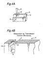
- Figs. 1A through 5B show the procedure for preparing a sample to be used in the transmission electron microscopic reaction process observation method according to this embodiment.
- the following describes a process of observing with a transmission electron microscope a silicification reaction between Ti(titanium) and a Si(silicon) substrate while it is heated.
- Fig. 4B shows an enlarged view of part A in Fig. 4A
- Fig. 5B shows an enlarged view of part C in Fig. 5A.
- a dice or piece of a size insertable in the transmission electron microscope is cut out of a wafer 1 prior to heat treatment by a dicing saw (not shown), whereby a sample 5 is obtained.
- the wafer 1 has been prepared by sputtering Ti 3 onto a Si substrate 2 and moreover continuously sputtering TiN (titanium nitride) 4 within the same chamber in order to prevent the Ti film 3 from oxidation or vaporization under vacuum or surface damage or the like.
- TiN titanium nitride
- a surface 7 (on the Ti film 3 side) of the sample 5 is cut to a depth of about 50 ⁇ m - 200 ⁇ m by a dicing saw 6, with a portion of a narrow width of about 5 ⁇ m - 50 ⁇ m left.
- the sample 5 is processed into an L-shape in cross section with a surface 7 side portion of width N (5 ⁇ m - 50 ⁇ m) ⁇ height 0 (50 ⁇ m - 200 ⁇ m) remaining like a post, as shown in Fig. 3.
- a Ga (gallium) ion beam 8 is applied by a convergent charged-particle beam equipment to the sample 5 along a side of a region 9 (which has a longitudinal length of 5 ⁇ m - 50 ⁇ m) in a narrow width portion 13 left on the surface 7 side of the sample 5.
- the surface 7 side of the sample in the region 9 is formed into a lamina of a thickness 50 nm - 200 nm which is small enough to allow the transmission electron microscopic observation to be effected.
- the sample 5 having the thus formed laminar portion 10 is fixed to a heatable holder (not shown) within the transmission electron microscope. Then, an electron beam is applied to penetrate the laminar portion 10 while the sample 5 is heated within the transmission electron microscope. In this situation, the manner how the Ti film 3 reacts with the Si substrate 2 to form silicide is observed through the transmission electron microscope.
- the sample 5 is taken out of the holder. Then, as shown in Fig. 5A, the Ga ion beam 8 is applied along a region 11, other than the region 9, of a sufficient thickness in the sample 5 by the convergent charged-particle beam equipment, so that the surface 7 side region is formed into a lamina having a thickness of 50 nm to 200 nm which is small enough to allow an observation by transmission electron microscopy to be effected.
- the sample 5 having the newly formed laminar portion 12 is then fixed to the holder for the transmission electron microscope. Then, electron beams are irradiated to penetrate the two laminar portions 10, 12 within the transmission electron microscope, and the two laminar portions 10 and 12 are observed in comparison with each other in a non-heated state.
- the silicide film has proved to be thicker in the laminar portion 10 than in the laminar portion 12, and to be stacked in multiple in the laminar portion 10.
- the laminar portion 12 which has been heated in its bulky state and afterwards formed into a lamina, represents a state of the sample heated in the form of wafer.
- the wafer 1 prior to being thermally treated is cut into a specified size to form the sample 5.
- the Ga ion beam 8 is applied to the region 9 on the surface 7 side of the sample 5, so that the sample 5 is formed into a lamina or thin film having a thickness of 50 nm - 200 nm small enough to enable the transmission electron microscopic observation.
- the obtained sample 5 is being heated within the transmission electron microscope, a reaction process in which silicification proceeds is observed.
- the Ga ion beam 8 is applied to a portion of a sufficient thickness of the sample 5 other than the laminar portion 10, whereby the other laminar portion 12 observable by transmission electron microscopy is formed.
- the laminar portions 10 and 12 of the sample 5 are observed in comparison with each other in a non-heated state by the transmission electron microscopy.
- the laminar portion 12 which has been heated in a thick film state, and the laminar portion 10 which has been heated in a thin film state are observed comparatively. And, if observation results of these laminar portions 10 and 12 are the same, it is inferred that the phenomenon observed in the laminar portion 10 during the heat treatment has occurred also in the bulk state. On the other hand, if observation results of the laminar portions 10 and 12 are different from each other, it is inferred that the phenomenon observed in the laminar portion 10 during the heat treatment is a unique phenomenon resulting from the heating of the sample in a thin film state, and that such a phenomenon does not occur in the bulk state.
- the present invention is applied to the observation of a reaction between a Ti film and a Si substrate into silicide.
- the present invention may be applied to the observation of various other phenomena such as reactions of Co(Cobalt)/Si, Ni(nickel)/Si or other Si compounds, reactions of Si crystals, movements of atoms in Al(aluminum) alloys or other metals, etc.
- the Ga ion beam 8 is applied during the formation of the laminar portion 10 and the laminar portion 12, the kind of the convergent charged-particle beam to be applied is not limited to this.
- the process of preparing a sample to be used for the reaction process observation by transmission electron microscopy according to the present invention is not limited to the one shown in Figs. 1A, 1B through Figs. 5A, 5B.
- the sample preparation method has only to be such that before and after the heat treatment, the same sample piece is thinned in different positions to a thickness on the order of several tens to several hundred nm which allows the thinned portions of the sample to transmit the electron beam.
Landscapes
- Engineering & Computer Science (AREA)
- Computer Hardware Design (AREA)
- Microelectronics & Electronic Packaging (AREA)
- General Engineering & Computer Science (AREA)
- Physics & Mathematics (AREA)
- General Physics & Mathematics (AREA)
- Sampling And Sample Adjustment (AREA)
- Analysing Materials By The Use Of Radiation (AREA)
- Testing Or Measuring Of Semiconductors Or The Like (AREA)
Claims (4)
- Verfahren zum Beobachten eines Reaktionsprozesses, der während einer Wärmebehandlung auftritt, unter Verwendung eines Transmissionselektronenmikroskops, umfassend:Bilden eines ersten laminaren Abschnitts (10) in einer Probe (5) durch Ausdünnen eines Teils (9) der Probe auf eine Dicke, die eine Transmission eines Elektronenstrahls (8) zulässt;Verbringen der Probe (5), die mit dem ersten laminaren Abschnitt (10) ausgebildet ist, in das Transmissionselektronenmikroskop und Durchführen einer Beobachtung mit dem Mikroskop an dem ersten laminaren Abschnitt, während die Probe einer Wärmebehandlung unterworfen wird;Herausnehmen der Probe (5) aus dem Transmissionselektronenmikroskop nach einer Beendigung der Wärmebehandlung und Bilden eines zweiten laminaren Abschnitts (12) in der Probe (5) durch ein Ausdünnen eines anderen Teils (11) der Probe als der erste laminare Abschnitt auf eine Dicke, die eine Transmission eines Elektronenstrahls (8) zulässt; undVerbringen der Probe, die mit den beiden laminaren Abschnitten (10, 12) ausgebildet ist, in das Transmissionselektronenmikroskop, und Durchführen einer Beobachtung mit dem Mikroskop an den zwei laminaren Abschnitten, ohne die Probe einer Wärmebehandlung zu unterwerfen.
- Verfahren nach Anspruch 1, dadurch gekennzeichnet, dass das Ausdünnen der Probe durch ein Anlegen eines konvergenten Strahls (8) geladener Partikel an die Probe erreicht wird.
- Verfahren nach Anspruch 1, weiter umfassend:vor einem Bilden des ersten laminaren Abschnitts (10) in der Probe, Beschichten einer Fläche der Probe mit einem Material (4), das mit einem Material (3) der Fläche der Probe während der Wärmebehandlung nicht reaktiv ist.
- Verfahren nach Anspruch 3, dadurch gekennzeichnet, dass das Material (3) der Fläche der Probe Titan ist und das Material (4), das die Fläche der Probe beschichtet, Titannitrid ist; und
ein Film aus Titan (3) und ein Film aus Titannitrid (4) kontinuierlich in dieser Reihenfolge gebildet werden.
Applications Claiming Priority (3)
| Application Number | Priority Date | Filing Date | Title |
|---|---|---|---|
| JP21304497 | 1997-08-07 | ||
| JP213044/97 | 1997-08-07 | ||
| JP21304497A JP3304836B2 (ja) | 1997-08-07 | 1997-08-07 | 透過型電子顕微鏡による反応プロセス観察方法 |
Publications (2)
| Publication Number | Publication Date |
|---|---|
| EP0899554A1 EP0899554A1 (de) | 1999-03-03 |
| EP0899554B1 true EP0899554B1 (de) | 2003-12-10 |
Family
ID=16632597
Family Applications (1)
| Application Number | Title | Priority Date | Filing Date |
|---|---|---|---|
| EP98306242A Expired - Lifetime EP0899554B1 (de) | 1997-08-07 | 1998-08-04 | Verfahren zur Beobachtung eines Reaktionsprozesses unter Verwendung der Transmissionselektronenmikroskopie |
Country Status (5)
| Country | Link |
|---|---|
| US (1) | US6005248A (de) |
| EP (1) | EP0899554B1 (de) |
| JP (1) | JP3304836B2 (de) |
| KR (1) | KR100290507B1 (de) |
| DE (1) | DE69820361T2 (de) |
Families Citing this family (3)
| Publication number | Priority date | Publication date | Assignee | Title |
|---|---|---|---|---|
| KR100558196B1 (ko) * | 2003-10-28 | 2006-03-10 | 삼성전자주식회사 | 투과전자현미경 검사용 시편을 고정시키기 위한 마운트 및이를사용하는 시편 제조 방법 |
| DE102005042075B3 (de) * | 2005-08-31 | 2007-01-04 | BAM Bundesanstalt für Materialforschung und -prüfung | Verfahren zur Präparation eines flächigen Probenkörpers sowie Präparat |
| US10265576B2 (en) * | 2014-10-06 | 2019-04-23 | Paul KAMINS | Lower body fitness apparatus for providing enhanced muscle engagement, body stability and range of motion |
Family Cites Families (9)
| Publication number | Priority date | Publication date | Assignee | Title |
|---|---|---|---|---|
| JPS62274237A (ja) * | 1986-05-23 | 1987-11-28 | Fujitsu Ltd | 電子顕微鏡用試料作成方法 |
| JP2504859B2 (ja) * | 1990-07-09 | 1996-06-05 | 日本電信電話株式会社 | 透過電子顕微鏡試料の作製方法 |
| JP3287858B2 (ja) * | 1991-05-15 | 2002-06-04 | 株式会社日立製作所 | 電子顕微鏡装置及び電子顕微方法 |
| JP2754301B2 (ja) * | 1992-01-07 | 1998-05-20 | シャープ株式会社 | 電子顕微鏡観察用試料の作成方法 |
| DE69406963T2 (de) * | 1993-03-15 | 1998-05-20 | Inoue, Akihisa, Sendai, Miyagi | Hochharte Dünnschicht, sowie Verfahren zu deren Herstellung |
| JP3221797B2 (ja) * | 1994-06-14 | 2001-10-22 | 株式会社日立製作所 | 試料作成方法及びその装置 |
| EP0735586B1 (de) * | 1995-03-28 | 2002-12-11 | Texas Instruments Incorporated | Halbleiterstrukturen |
| JP3485707B2 (ja) * | 1996-01-09 | 2004-01-13 | 沖電気工業株式会社 | 透過型電子顕微鏡用の平面サンプルの作製方法及びその透過型電子顕微鏡による欠陥測定方法 |
| JP3321533B2 (ja) * | 1996-08-27 | 2002-09-03 | シャープ株式会社 | 透過型電子顕微鏡用試料作製方法 |
-
1997
- 1997-08-07 JP JP21304497A patent/JP3304836B2/ja not_active Expired - Fee Related
-
1998
- 1998-08-03 US US09/127,867 patent/US6005248A/en not_active Expired - Fee Related
- 1998-08-04 EP EP98306242A patent/EP0899554B1/de not_active Expired - Lifetime
- 1998-08-04 DE DE69820361T patent/DE69820361T2/de not_active Expired - Fee Related
- 1998-08-05 KR KR1019980031839A patent/KR100290507B1/ko not_active Expired - Fee Related
Also Published As
| Publication number | Publication date |
|---|---|
| EP0899554A1 (de) | 1999-03-03 |
| DE69820361D1 (de) | 2004-01-22 |
| JP3304836B2 (ja) | 2002-07-22 |
| KR19990023370A (ko) | 1999-03-25 |
| DE69820361T2 (de) | 2004-09-23 |
| US6005248A (en) | 1999-12-21 |
| JPH1154578A (ja) | 1999-02-26 |
| KR100290507B1 (ko) | 2001-06-01 |
Similar Documents
| Publication | Publication Date | Title |
|---|---|---|
| KR100451604B1 (ko) | 주사전자현미경 시료 제조 방법 및 반도체 장치 해석 방법 | |
| Chang et al. | Transmission electron microscopy of gold‐silicon interactions on the backside of silicon wafers | |
| EP0899554B1 (de) | Verfahren zur Beobachtung eines Reaktionsprozesses unter Verwendung der Transmissionselektronenmikroskopie | |
| US5935870A (en) | Top view TEM sample preparation method | |
| US6723650B1 (en) | TEM sample preparation using transparent defect protective coating | |
| Rebhan et al. | Low-temperature aluminum-aluminum wafer bonding | |
| EP4297069A1 (de) | Verbundwafer und herstellungsverfahren dafür | |
| US7355176B2 (en) | Method of forming TEM specimen and related protection layer | |
| KR100558196B1 (ko) | 투과전자현미경 검사용 시편을 고정시키기 위한 마운트 및이를사용하는 시편 제조 방법 | |
| Madsen et al. | Influence of material properties on TEM specimen preparation of thin films | |
| JP2000230891A (ja) | 透過型電子顕微鏡用試料の作製方法 | |
| US7297950B2 (en) | Transmission electron microscope specimen and method of manufacturing the same | |
| Park et al. | Interface characterization of epitaxial ag films on si (100) and si (111) grown by molecular beam epitaxy | |
| Anderson et al. | Practical aspects of FIB TEM specimen preparation: With emphasis on semiconductor applications | |
| KR20050112261A (ko) | 투과전자현미경 분석용 시편의 제작 방법. | |
| Kawasaki et al. | A new specimen preparation method for cross-section TEM using diamond powders | |
| Tsujimoto et al. | Cross-sectional TEM sample preparation method using FIB etching for thin-film transistor | |
| Ivey et al. | Radiation damage effects in GaAs transmission electron microscopy specimens prepared by ion milling | |
| KR20070054811A (ko) | 2종의 분석 현미경에 적용되는 분석시편의 제작 방법 | |
| KR100506827B1 (ko) | 시편의 딤플 형성방법 및 이를 이용한 투과전자 현미경용시편의 제작방법 | |
| Gibbesch et al. | Ultrahigh vacuum diffusion bonding of metals to ceramics | |
| Chang et al. | Cross-sectional TEM sample preparation for multilayer electronic materials | |
| Vanhellemont et al. | A rapid specimen preparation technique for cross-section TEM investigation of semiconductors and metals | |
| Susnitzky et al. | Metal particles on the surfaces of heat-treated ceramic thin films | |
| KR100683115B1 (ko) | 투과전자현미경용 시편 및 이의 제조 방법 |
Legal Events
| Date | Code | Title | Description |
|---|---|---|---|
| PUAI | Public reference made under article 153(3) epc to a published international application that has entered the european phase |
Free format text: ORIGINAL CODE: 0009012 |
|
| AK | Designated contracting states |
Kind code of ref document: A1 Designated state(s): DE FR GB NL |
|
| AX | Request for extension of the european patent |
Free format text: AL;LT;LV;MK;RO;SI |
|
| 17P | Request for examination filed |
Effective date: 19990521 |
|
| AKX | Designation fees paid |
Free format text: DE FR GB NL |
|
| GRAH | Despatch of communication of intention to grant a patent |
Free format text: ORIGINAL CODE: EPIDOS IGRA |
|
| GRAH | Despatch of communication of intention to grant a patent |
Free format text: ORIGINAL CODE: EPIDOS IGRA |
|
| GRAA | (expected) grant |
Free format text: ORIGINAL CODE: 0009210 |
|
| AK | Designated contracting states |
Kind code of ref document: B1 Designated state(s): DE FR GB NL |
|
| REG | Reference to a national code |
Ref country code: GB Ref legal event code: FG4D |
|
| REF | Corresponds to: |
Ref document number: 69820361 Country of ref document: DE Date of ref document: 20040122 Kind code of ref document: P |
|
| ET | Fr: translation filed | ||
| PLBE | No opposition filed within time limit |
Free format text: ORIGINAL CODE: 0009261 |
|
| STAA | Information on the status of an ep patent application or granted ep patent |
Free format text: STATUS: NO OPPOSITION FILED WITHIN TIME LIMIT |
|
| 26N | No opposition filed |
Effective date: 20040913 |
|
| PGFP | Annual fee paid to national office [announced via postgrant information from national office to epo] |
Ref country code: NL Payment date: 20080815 Year of fee payment: 11 Ref country code: DE Payment date: 20080814 Year of fee payment: 11 |
|
| PGFP | Annual fee paid to national office [announced via postgrant information from national office to epo] |
Ref country code: FR Payment date: 20080818 Year of fee payment: 11 |
|
| PGFP | Annual fee paid to national office [announced via postgrant information from national office to epo] |
Ref country code: GB Payment date: 20080813 Year of fee payment: 11 |
|
| REG | Reference to a national code |
Ref country code: NL Ref legal event code: V1 Effective date: 20100301 |
|
| GBPC | Gb: european patent ceased through non-payment of renewal fee |
Effective date: 20090804 |
|
| REG | Reference to a national code |
Ref country code: FR Ref legal event code: ST Effective date: 20100430 |
|
| PG25 | Lapsed in a contracting state [announced via postgrant information from national office to epo] |
Ref country code: NL Free format text: LAPSE BECAUSE OF NON-PAYMENT OF DUE FEES Effective date: 20100301 Ref country code: FR Free format text: LAPSE BECAUSE OF NON-PAYMENT OF DUE FEES Effective date: 20090831 Ref country code: DE Free format text: LAPSE BECAUSE OF NON-PAYMENT OF DUE FEES Effective date: 20100302 |
|
| PG25 | Lapsed in a contracting state [announced via postgrant information from national office to epo] |
Ref country code: GB Free format text: LAPSE BECAUSE OF NON-PAYMENT OF DUE FEES Effective date: 20090804 |