EP0884818B1 - Procédé de commande d'au moins un transistor du type IBGT apte à permettre le fonctionnement de celui-ci sous irradiation - Google Patents
Procédé de commande d'au moins un transistor du type IBGT apte à permettre le fonctionnement de celui-ci sous irradiation Download PDFInfo
- Publication number
- EP0884818B1 EP0884818B1 EP98401379A EP98401379A EP0884818B1 EP 0884818 B1 EP0884818 B1 EP 0884818B1 EP 98401379 A EP98401379 A EP 98401379A EP 98401379 A EP98401379 A EP 98401379A EP 0884818 B1 EP0884818 B1 EP 0884818B1
- Authority
- EP
- European Patent Office
- Prior art keywords
- transistor
- igbt
- vge
- voltage
- threshold voltage
- Prior art date
- Legal status (The legal status is an assumption and is not a legal conclusion. Google has not performed a legal analysis and makes no representation as to the accuracy of the status listed.)
- Expired - Lifetime
Links
Images



Classifications
-
- H—ELECTRICITY
- H02—GENERATION; CONVERSION OR DISTRIBUTION OF ELECTRIC POWER
- H02H—EMERGENCY PROTECTIVE CIRCUIT ARRANGEMENTS
- H02H5/00—Emergency protective circuit arrangements for automatic disconnection directly responsive to an undesired change from normal non-electric working conditions with or without subsequent reconnection
- H02H5/005—Emergency protective circuit arrangements for automatic disconnection directly responsive to an undesired change from normal non-electric working conditions with or without subsequent reconnection responsive to ionising radiation; Nuclear-radiation circumvention circuits
Definitions
- the present invention relates to a method for controlling at least one transistor of the IGBT type capable to allow the operation of it under irradiation.
- IGBT transistors Insulated Gate Bipolar Transistor
- bipolar transistor with insulated gate In order to be able to control a motor “Brushless”, or any other current motor alternative, we are faced with power supplies from 400 to 1000 volts requiring the use of IGBT transistors (“Insulated Gate Bipolar Transistor” or bipolar transistor with insulated gate).
- This second strategy is the one that is considered in the process of the invention, because it is the only one to obtain the dose uniforms that we are trying to achieve.
- Different studies conducted on the behavior of N-MOS transistors under radiation ⁇ made it possible to highlight the drift of the threshold voltage Vgs towards negative voltages following the integrated dose before reaching a negative asymptote.
- a second solution of hardening system therefore consists in ordering the switching of the N-MOS transistor using two tensions: a positive to make it totally passing and a negative to be able to block it whatever the drift of its threshold voltage Vgs.
- a system hardening solution is therefore necessary for each type of transistor. Of more, it is necessary to know, for each series of each semiconductor manufacturer, the precise behavior of each transistor considered even if we are able to predict the main directions drifts of the characteristics concerned.
- the subject of the invention is a method of command for mounting a power, based on IGBT transistor, whose resistance to the cumulative dose is established above 10 Mrad (100 Kgy).
- the present invention provides a method of controlling at least one transistor of the IGBT type capable of allowing its operation under irradiation, characterized in that the threshold value Vge s of the grid-emitter voltage of a first IGBT transistor under irradiation and the voltage applied in operation between the gate and the emitter is varied by at least one second IGBT transistor under irradiation so as to control the threshold voltage Vge s of this second transistor (s) ( s) IGBT at a set value despite the drift caused by the irradiation.
- the measurement of the control signal is carried out on a IGBT test transistor.
- At least one of the two is modulated power sources, respectively positive and negative, applied between grid and transmitter of a (or second IGBT transistor (s).
- the second IGBT transistor (s) is (are) subject to double switching: conventional switching in blocked-unlocked and switching the amplitude of the threshold voltage Vge applied between gate and emitter for the implementation of the control according to the invention.
- Figure 1 illustrates an equivalent diagram an IGBT transistor, which is characterized by a input MOS transistor (transistor T1) and a PNP bipolar transistor at output (transistor T2).
- transistor T1 input MOS transistor
- PNP bipolar transistor at output transistor T2
- Vge positive MOS transistor
- an electric field is created across the insulation under the grid. This electric field allows an inversion of the P doping towards an N doping, under the insulation layer.
- the integrated dose affects mainly these by two phenomena of trapping.
- the first trap of holes in the oxides and the second results from their migration to the interface Si-SiO2.
- the consequence is the negative drift of threshold voltages of the MOS transistors.
- the variation of the threshold voltage is the result of several phenomena, which have opposing effects, with different kinetics depending on the temperature and polarization.
- a specific test card 20 makes it possible to maintain the transistors at a constant distance from the source.
- An analog multiplexer 21 of the AMUX64T (National Instrument) type makes it possible to select the channels and to convert the analog data into digital (CAN), as well as to supply the test signals.
- a square signal generator 22 of frequency 12 kHz and voltage ⁇ 15 volts is used to power the transistors between the measurements.
- a computer 23 with specific software controls all of the measurements and saves the results on a hard disk 24. The measurements are performed every 20 minutes. Between each measurement, the transistors switch thanks to generator 12.
- the tests are carried out for a current of 100 mA.
- the value of the corresponding voltage Vge is determined by successive approximations.
- the dose rate is set at 100 Gy / H, which makes it possible to exceed 10 kGy of cumulative dose after one week.
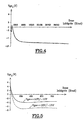
- the graph in FIG. 3 represents the evolution of the drift of the threshold voltage Vge s for almost all of the IGBT transistors tested.
- the latter is divided into three distinctive phases.
- the appearance of phase 2 and phase 3 may occur sooner or later compared to the dose absorbed depending on the type of IGBT transistor concerned.
- the amplitude of the three phases depends on the type of IGBT transistor tested.
- the irradiation begins with the predominance of trapping of charges in the insulator, and in particular of holes which remain in an area relatively close to their trapping site, the electrons trapped being quickly evacuated. There is therefore a contribution of positive charges in the insulation between the grid and the channel area.
- a lower voltage Vge must be applied than previously. The threshold voltage Vge s then drifts downward towards negative voltages.
- charge trapping can be compensated for and then overcome by other contrary effects which are the following:
- the first effect, or interface effect, comes from the MOS part of the IGBT transistor. AT the interface between the insulator and the semiconductors doped new interface states appear where negative charges partially offset the positive charges trapped.
- the second effect comes from the part bipolar (PNP) of the IGBT transistor.
- PNP part bipolar
- a degradation of gain ⁇ occurs, as for the MOS transistor, because the appearance of new interface states between doped insulator and semiconductor. These new states of interfaces introduce an acceleration of the charge carrier recombination speed minority and ultimately reduce the gain.
- This gain degradation comes primarily from the ionization of the oxide at the interfaces covering the base-emitter region of the PNP transistor.
- the third effect which also comes from the PNP bipolar transistor, is characterized by the increase in the leakage currents of the PNP transistor.
- This increase in leakage currents at the interfaces with the insulator mainly takes place in the region of the insulator covering the collector-base junction of the PNP transistor, that is to say in the same places as the degradations and new states of interfaces involved in the MOS part.
- This increase in leakage currents facilitates blocking of the IGBT transistor, and raises the threshold voltage Vge s .
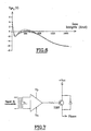
- the graph in Figure 6 shows the dispersion of the results in a same batch of components. To be able to use these transistors, it is essential to observe a homogeneous behavior of the components of the same batch. In general, the resistance to radiation depends a lot on the manufacturing process components. If this varies from batch to batch, the characterizations must be renewed. Of the same two components with the same reference in two different manufacturers should be considered separately.
- the main characteristic to be mastered is the blocking voltage of these transistors, or threshold voltage, Vge s .
- the invention consists in measuring the evolution of the drift of the threshold voltage Vge s via an IGBT transistor and in following the amplitude of the two power supplies of the grid accordingly (Vp for its positive voltage; Vn for its negative voltage).
- Vp for its positive voltage
- Vn for its negative voltage
- the invention also consists in measuring the threshold value Vge s of the gate-emitter voltage of a first IGBT transistor under irradiation and in varying the applied voltage in operation between gate and emitter of at least one second IGBT transistor under irradiation so as to control the threshold voltage Vge s of this IGBT transistor (s) to a set value despite the drift generated by the irradiation.
- the first transistor may be an IGBT test transistor. It is possible to modulate at least one of the two power sources, respectively positive Vp and negative Vn applied between the gate and the emitter of the second IGBT transistor (s).
- the system for monitoring the Vp and Vn supplies is simplified by considering a system for switching only the supply Vp with respect to a reference -X of drift of the threshold voltage Vge s .
- This simplification is designed as a more "logical" solution compared to the original analog solution only.
- the evolution of the threshold voltage drift makes it possible to simplify and make the circuit more reliable, an analog circuit being more sensitive to an irradiation dose than a circuit composed of logic gates (provided that the technology is properly selected employee).
- the invention makes it possible to control the drift of the threshold voltage Vge s to the chosen reference voltage.
- the choice of this reference (-X) is then a parameter for optimizing the system.
- a basic control assembly of a IGBT transistor in a power bridge, illustrated on Figure 7 highlights the action of the two voltages Vp and Vn which set the voltage levels of the switching initiated by the control signal.
- the invention does not take into account that the voltage Vp to harden the transistor IGBT.
- the drift of the threshold voltage Vge s is then controlled by acting on the value of the positive voltage Vp applied to the gate of the IGBT transistor making it passing during operation in switching mode.
- This voltage Vp is given a more or less important value according to the evolution of the value of the voltage Vge s as the radiation dose cumul is accumulated.
- This slaving is carried out on the basis of the measurement of the voltage Vge s for example on a test IGBT transistor, which therefore controls and slaves the drifts of the threshold voltages Vge s of the other transistors, which are all identical. Another example could be to make the measurement directly on the transistor without disturbing the application.
- This simple positive supply switching makes it possible to enslave the drift of Vge s around - X and thus ensures the durability of the circuit with respect to the accumulation of the dose received.
- the IGBT transistor receives a double switching: the switching making it on or off and the switching of the amplitude of its positive opening voltage providing it with a controlled asymptote of the drift of its threshold voltage Vge s .
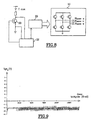
- FIG. 8 A general block diagram implementing a such a process is illustrated in Figure 8.
- the IGBT test transistor 30 is represented in the figure, a circuit 31 comprising six other IGBT transistors (Q1 to Q6), a module 32 for measuring and comparing the voltage -X, and a module 33 for calculating the voltage positive Vp.
- the curve of the drift of the voltage Vge s with respect to the cumulative dose shows a control of the drift around the reference considered.
- the invention makes it possible to produce a power amplifier for brushless motor (in other words, self-piloting synchronous motor), using a "hardened" three-phase power bridge at base of IGBT transistors, especially in the application to a robot operating in a nuclear environment.
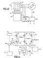
- This amplifier is capable of supplying a current of 10 A under a voltage of 200 volts. As illustrated in the Figure 10, it includes a voltage inverter 40, the command 41 thereof by the method of the invention, a module 42 for monitoring currents, and a reference current generation module 43, PR corresponding to the position of the rotor.
- the amplifier considered consists of two superimposed cards: a power card which includes the power bridge, the test transistor and associated commands, and a command card which combines the feeds, the sequencing and all the logic useful for the operation of the amplifier.
- FIG. 11 illustrates the block diagram of the power card.
- This card contains a power bridge 45 of six IGBT transistors Q1 to Q6, as well as the “Drivers” stages 46 and the respective power supply secondary 48, galvanically isolated.
- FIG. 11 illustrates the control of a single IGBT transistor, Q 4 . But the other five IGBT transistors are controlled in the same way.
- This card also contains an IGBT test transistor 49 which is in operating conditions comparable (in particular the same temperature) to that of the transistors of the power bridge 45.
- a logic control module 50 In this figure are also represented a logic control module 50, a module 51 supply of the voltages Vp and Vn galvanically isolated, a module 52 for measuring time, a driver stage 53, a relay measurement 54 and a module 55 for measuring the threshold voltage Vge s .
- the control card 60 groups together all digital parts of the amplifier considered.
- This card contains in particular the whole system hardening logic (synchronization, measurement and processing), the modulation of the orders of switching of the different bridge transistors, as well that the cutting of the power supplies of the grids of IGBT transistors in order to isolate them galvanically by transformers.
- This card includes a module synchronization 61, a switching relay power supply Vp 62, a power supply module 63, and a modulation module 64.
- the modulation module synchronization 61 is connected to the test transistor 49 and to the measurement relay 54.
- the modulation module 64 and the power module are connected to the power 66, the modulation module also being connected to the control module 50.
Landscapes
- Physics & Mathematics (AREA)
- High Energy & Nuclear Physics (AREA)
- Electronic Switches (AREA)
- Testing Of Individual Semiconductor Devices (AREA)
Description
- On peut utiliser des composants durcis provenant des filières militaires. Cependant ces filières n'offrent que des composants coûteux et uniquement capables de tenir des doses cumulées relativement faibles comparées aux doses cumulées prévues pour les équipements du nucléaire civil. D'autre part aucun transistor IGBT n'est à l'heure actuelle disponible dans-sa version durcie. Enfin, on peut penser que, suite à la décroissance générale de tous les budgets militaires, les filières des composants durcis seront amenées à disparaítre à plus ou moins long terme.
- On peut n'utiliser que des composants des grandes séries du commerce et tenir compte, voire contrôler leurs éventuelles dérives. C'est ce que l'on appelle le durcissement système. Cette stratégie nécessite de bien connaítre le comportement de chaque composant lors de son irradiation.
- il permet d'atteindre des tenues à des doses d'irradiation très importantes du point de vue de l'étage de puissance (> 100 kGy) étant donné que la dérive est compensée. Il permet de concevoir des ensembles électroniques durcis sans que la partie puissance soit l'élément contraignant du point de vue de la dose reçue ;
- il permet d'obtenir un gain en rendement (ce qui est important du point de vue de l'électronique de puissance) vis-à-vis de l'utilisation de simples alimentations symétriques de fortes valeurs. Lors de la commutation d'alimentation positive de +2α à +α, la perte d'énergie nécessaire à la commande du transistor est divisée par deux ;
- il est applicable à tous les transistors IGBT du marché quel que soit leur fabriquant, à condition de prévoir quelques tests préalables ;
- il permet d'optimiser le circuit considéré dans son ensemble, car on connaít -X à l'avance.
- dans les amplificateur de puissance pour moteur « Brushless » pour la robotique utilisant des transistors IGBT comme interrupteurs de puissance ;
- dans les ponts de puissance triphasés pour tous les moteurs à courant alternatif (asynchrones, ..) ;
- dans les alimentations utilisant des transistors IGBT.
- La figure 1 illustre le schéma équivalent d'un transistor IBGT ;
- la figure 2 illustre le synoptique d'un banc de test utilisé ;
- la figure 3 illustre l'effet de la dose cumulée sur un transistor IGBT ;
- la figure 4 illustre le comportement à forte dose d'un transistor IGBT ;
- la figure 5 illustre l'influence de la polarisation sur le fonctionnement d'un transistor IGBT ;
- la figure 6 illustre la dispersion des résultats sur un lot de transistors IGBT ;
- la figure 7 illustre le montage de base de commande d'un transistor IGBT dans un pont de puissance ;
- la figure 8 illustre le synoptique général d'un dispositif mettant en oeuvre le procédé de l'invention ;
- la figure 9 illustre les résultats de tests en commutation d'alimentations positives ;
- la figure 10 illustre un synoptique d'un amplificateur destiné à piloter un moteur « Brushless » pour robot ;
- la figure 11 illustre le synoptique de la carte de puissance de l'amplificateur illustré sur la figure 10 ;
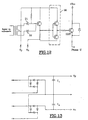
- la figure 12 illustre un module « Driver » de la carte de puissance illustrée sur la figure 11 ;
- la figure 13 illustre un autre module de la carte de puissance illustrée sur la figure 11 ;
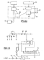
- la figure 14 illustre le synoptique de la carte de commande de l'amplificateur illustré sur la figure 10 ;
- la figure 15 illustre un module permettant la synchronisation et la mesure du signal de seuil Vges dans la carte de commande illustrée sur la figure 14 ;
- la figure 16 illustre cette synchronisation et cette mesure ;
- la figure 17 illustre le module d'alimentation de la commande dans la carte de commande illustrée sur la figure 14 ;
- la figure 18 illustre le module permettant la modulation dans la carte de commande illustrée sur la figure 14.
- L'influence de la polarisation positive. Comme décrit précédemment : au regard de la figure 5, plus la polarisation de la grille du transistor IGBT est faible, moins sa tension de seuil Vges a tendance à dériver vers les tensions négatives.
- Le rendement général du montage. La puissance consommée pour commander le transistor diffère suivant les valeurs des tensions appliquées.
- Le pilote (module Driver 46), illustré sur la figure 12, qui permet la commande directe d'un transistor IGBT à partir de l'information logique obtenue en sortie du module 50. Une démodulation est réalisée par deux diodes D1 et D2 de type « Schottky » montées en redresseurs avec point milieu. Le signal ainsi redressé attaque un amplificateur 56 de type « Push-Pull ».
- Le secondaire 48 d'alimentation de la grille du transistor IGBT considéré, comme illustré sur la figure 13, qui est constitué d'une part d'un étage de redressement réalisé par des diodes de type « Schottky », par exemple de type 1N5819, pour limiter la chute de tension et d'autre part, d'un filtrage réalisé par deux condensateurs (C1, C2). On obtient ainsi deux tensions Vp et Vn qui alimentent l'étape de puissance.
- La synchronisation et la mesure de la tension de seuil Vges : le module 61 permettant cette synchronisation et cette mesure, qui est illustré sur la figure 15, contient tout le séquencement du durcissement système mis en place dans l'amplificateur considéré. Ce module comprend notamment des circuits NON-ET-trigger 67, 68, 69, 70 et 71, des circuits monostables 72 et 73 de type 74LS123, et une bascule D 74. Le séquencement réalisé, illustré sur la figure 16, est le suivant : on génère toutes les quinze minutes (V1) une impulsion de 100 ms (V2). Le front montant de cette impulsion vient déclencher le relais 54 de la carte puissance. Il en découle l'arrêt de la commutation du transistor IGBT de test 49 et la polarisation négative de sa tension de grille sous-1.75 volts. Pendant les 100 ms de l'impulsion, on crée un retard de 20 ms (V3) afin de laisser le temps au relais d'effectuer son changement d'état. Puis pendant 60 ms (V4) on effectue la mesure de la tension Vces du transistor de test 49 afin de connaítre son état (bloqué ou saturé). Selon l'état constaté on donne l'ordre, ou non, au relais de commande des alimentations positives 62 de basculer. Tout comme l'horloge (T = 15 minutes) l'impulsion de 100 ms est réalisée à l'aide d'une porte NON-ET-trigger 67. Les retards de 20 ms et 60 ms sont réalisés à l'aide de circuits monostables 72 et 73.
- L'alimentation de la commande : le module 63 permettant cette alimentation, qui est illustré sur la figure 17, génère un découpage primaire des alimentations positives et négatives des grilles des transistors IGBT du pont de puissance. Ce découpage, réalisé à l'aide de deux circuit intégrés de puissance 75 et 76 par exemple de type unitrode UC3707, permet d'attaquer les transformateurs d'alimentation. Ces derniers sont alimentés par une tension qui est commutée par le relais de commutation d'alimentation 62. L'horloge de modulation (f = 595 Hz) est fabriquée par un oscillateur à trigger de Schmitt 77 et une bascule D 78 montée en diviseur par deux. L'horloge de modulation a un rapport cyclique de 50 % pour éviter les composantes continues dans le transformateur.
- La modulation : le module 64 récupérant l'horloge du module d'alimentation de la commande, qui est illustré sur la figure 18 a pour unique fonction de moduler la commande des transistors IGBT du pont de puissance afin de pouvoir alimenter les transformateurs de commande. La modulation est réalisée par des portes logiques ET 80, 81, 82, 83 qui reçoivent le signal de commande du transistor et l'horloge issue du trigger de Schmitt 77.
Claims (8)
- Procédé de commande d'au moins un transistor de type IGBT apte à permettre un fonctionnement de celui-ci sous irradiation, caractérisé en ce qu'on mesure la valeur de seuil Vges de la tension grille-émetteur d'un premier transistor IGBT (30) sous irradiation et on fait varier la tension appliquée en fonctionnement entre grille et émetteur d'au moins un second transistor IGBT (Q1-Q6) sous irradiation de manière à asservir la tension de seuil Vges de ce (s) transistor (s) IGBT à une valeur de consigne malgré la dérive engendrée par l'irradiation.
- Procédé selon la revendication 1, dans lequel le premier transistor (30) est un transistor IGBT de test.
- Procédé selon la revendication 1, dans lequel on module au moins l'une des deux sources d'alimentation, respectivement positive Vp et négative Vn, appliquées entre grille et émetteur du (ou des) second(s) transistor(s) IGBT.
- Procédé selon la revendication 3, dans lequel le (ou les) second(s) transistor(s) IGBT est (sont) ainsi soumis à une double commutation : une commutation classique en bloqué-débloqué et une commutation de l'amplitude de la tension de seuil Vge pour la mise en oeuvre de l'asservissement.
- Procédé selon la revendication 4, dans lequel on commute la tension positive Vp appliquée suivant la valeur de la tension de seuil Vges du premier transistor (30) par rapport à un repère -X, de la manière suivante, α étant une valeur de tension déterminée :
Si Vges > -X alors Vp = +2α
Si Vges < -X alors Vp = +α
ce qui permet d'assurer une asymptote contrôlée de sa tension de seuil Vges. - Procédé selon la revendication 5, dans lequel on a : α = 5 volts.
- Utilisation du procédé selon l'une quelconque des revendications précédentes pour réaliser un variateur de puissance pour moteur « Brushless », en utilisant un pont de puissance triphasé durci à base de transistors IGBT.
- Utilisation du procédé selon l'une quelconque des revendication 1 à 6, pour réaliser l'alimentation de puissance de moteurs asynchrones.
Applications Claiming Priority (2)
| Application Number | Priority Date | Filing Date | Title |
|---|---|---|---|
| FR9707238A FR2764713B1 (fr) | 1997-06-11 | 1997-06-11 | Procede de commande d'au moins un transistor du type igbt apte a permettre le fonctionnement de celui-ci sous irradiation |
| FR9707238 | 1997-06-11 |
Publications (2)
| Publication Number | Publication Date |
|---|---|
| EP0884818A1 EP0884818A1 (fr) | 1998-12-16 |
| EP0884818B1 true EP0884818B1 (fr) | 2001-08-22 |
Family
ID=9507856
Family Applications (1)
| Application Number | Title | Priority Date | Filing Date |
|---|---|---|---|
| EP98401379A Expired - Lifetime EP0884818B1 (fr) | 1997-06-11 | 1998-06-09 | Procédé de commande d'au moins un transistor du type IBGT apte à permettre le fonctionnement de celui-ci sous irradiation |
Country Status (5)
| Country | Link |
|---|---|
| US (1) | US5969569A (fr) |
| EP (1) | EP0884818B1 (fr) |
| JP (1) | JPH1155098A (fr) |
| DE (1) | DE69801397T2 (fr) |
| FR (1) | FR2764713B1 (fr) |
Families Citing this family (10)
| Publication number | Priority date | Publication date | Assignee | Title |
|---|---|---|---|---|
| FR2785713B1 (fr) * | 1998-11-10 | 2000-12-08 | Commissariat Energie Atomique | Systeme de commande d'unites de levage et de telemanipulation placees en enceinte confinee |
| FR2790327B1 (fr) * | 1999-02-26 | 2001-04-13 | Commissariat Energie Atomique | Systeme electronique fonctionnant sous irradiation, procede de conception d'un tel systeme, et application de celui-ci a la commande d'un robot mobile |
| US7085088B2 (en) * | 2002-05-23 | 2006-08-01 | Texas Instruments Incorporated | Method of controlling reader amplifier gain variations of a HDD preamplifier, or the like |
| US6927988B2 (en) * | 2002-05-28 | 2005-08-09 | Ballard Power Systems Corporation | Method and apparatus for measuring fault diagnostics on insulated gate bipolar transistor converter circuits |
| DE10236532C1 (de) * | 2002-08-09 | 2003-08-14 | Semikron Elektronik Gmbh | Schaltungsanordnung zur Ansteuerung von Leistungstransistoren |
| WO2011071573A2 (fr) * | 2009-09-02 | 2011-06-16 | Arizona Board Of Regents, For And On Behalf Of Arizona State University | Amplificateurs comprenant des transistors à film mince à appauvrissement et enrichissement et procédés associés |
| FR2982092B1 (fr) * | 2011-11-02 | 2015-01-02 | Valeo Systemes De Controle Moteur | Module de puissance et dispositif electrique pour l'alimentation et la charge combinees respectivement d'un accumulateur et d'un moteur |
| CN111046529B (zh) * | 2019-11-20 | 2022-11-04 | 中南大学 | 一种igbt的老化建模方法及老化注入器 |
| CN111008506B (zh) * | 2019-11-30 | 2023-04-07 | 中国科学院新疆理化技术研究所 | 一种基于阈值电压类型匹配的6-t存储单元抗总剂量加固方法 |
| US20240339826A1 (en) * | 2021-07-30 | 2024-10-10 | Airbus Defence And Space Sas | Electronic spatial system |
Family Cites Families (1)
| Publication number | Priority date | Publication date | Assignee | Title |
|---|---|---|---|---|
| EP0838855B1 (fr) * | 1991-09-20 | 2004-11-24 | Hitachi, Ltd. | Module semi-conducteur |
-
1997
- 1997-06-11 FR FR9707238A patent/FR2764713B1/fr not_active Expired - Fee Related
-
1998
- 1998-06-09 EP EP98401379A patent/EP0884818B1/fr not_active Expired - Lifetime
- 1998-06-09 DE DE69801397T patent/DE69801397T2/de not_active Expired - Fee Related
- 1998-06-11 JP JP10163993A patent/JPH1155098A/ja not_active Withdrawn
- 1998-06-11 US US09/095,584 patent/US5969569A/en not_active Expired - Fee Related
Also Published As
| Publication number | Publication date |
|---|---|
| DE69801397D1 (de) | 2001-09-27 |
| DE69801397T2 (de) | 2002-05-02 |
| FR2764713B1 (fr) | 1999-07-16 |
| JPH1155098A (ja) | 1999-02-26 |
| US5969569A (en) | 1999-10-19 |
| FR2764713A1 (fr) | 1998-12-18 |
| EP0884818A1 (fr) | 1998-12-16 |
Similar Documents
| Publication | Publication Date | Title |
|---|---|---|
| EP2276173B1 (fr) | Dispositif de commande d'un transistor de puissance | |
| EP0409697B1 (fr) | Circuit intégré MOS à tension de seuil ajustable | |
| EP0378453B1 (fr) | Générateur de tension de référence stable | |
| US7388183B2 (en) | Low dark current pixel with a guard drive active photodiode | |
| EP0884818A1 (fr) | Procédé de commande d'au moins un transistor du type IBGT apte à permettre le fonctionnement de celui-ci sous irradiation | |
| WO2011117781A1 (fr) | Procédé et dispositif de contremesure pour protéger des données circulant dans un microcircuit électronique | |
| FR2717918A1 (fr) | Circuit pour contrôler les tensions entre caisson et sources des transistors mos et système d'asservissement du rapport entre les courants dynamique et statique d'un circuit logique mos. | |
| FR2714547A1 (fr) | Système de commande d'actionneurs à courant continu en électronique de puissance. | |
| FR2510781A1 (fr) | Generateur de tension de reference | |
| FR2492607A1 (fr) | Dispositif de commande de vitesse pour un moteur a courant continu | |
| CH632610A5 (fr) | Source de tension de reference realisee sous forme d'un circuit integre a transistors mos. | |
| EP0014149B1 (fr) | Générateur de tension de référence et circuit de mesure de la tension de seuil de transistor MOS, applicable à ce générateur de tension de référence | |
| TWI813621B (zh) | 恢復輻射檢測器的方法 | |
| WO2006103333A2 (fr) | Commande de transistors mos | |
| FR2580443A1 (fr) | Amplificateur en courant continu rapide pouvant etre deconnecte avec une compensation de courant de polarisation a l'etat deconnecte | |
| FR3013920A1 (fr) | Dispositif electronique de commutation avec reduction des courants de fuite et procede de commande correspondant | |
| WO2023214122A1 (fr) | Dispositif et procédé de caractérisation de l'effondrement de courant de transistors gan | |
| FR2647280A1 (fr) | Alimentation en courant synchronisee en mode commute | |
| EP0981203A1 (fr) | Source de courant contrôlée à commutation accélérée | |
| FR2896643A1 (fr) | Dispositif de commande d'un transistor mos | |
| JPH0448735A (ja) | 薄膜トランジスタの特性安定化手法 | |
| EP0628827B1 (fr) | Circuit intégré comportant un circuit de détection du niveau d'une tension de service | |
| EP1473755A2 (fr) | Dispositif et procédé de commande et de contrôle d'une dose d'électrons émise par un micro-émetteur | |
| JP2010074041A (ja) | フォトダイオード及びそれを備えた集積化受光素子 | |
| FR2958098A1 (fr) | Procede et dispositif de contremesure pour proteger des donnees circulant dans un microcircuit electronique |
Legal Events
| Date | Code | Title | Description |
|---|---|---|---|
| PUAI | Public reference made under article 153(3) epc to a published international application that has entered the european phase |
Free format text: ORIGINAL CODE: 0009012 |
|
| AK | Designated contracting states |
Kind code of ref document: A1 Designated state(s): BE DE GB IT |
|
| AX | Request for extension of the european patent |
Free format text: AL;LT;LV;MK;RO;SI |
|
| 17P | Request for examination filed |
Effective date: 19990604 |
|
| AKX | Designation fees paid |
Free format text: BE DE GB IT |
|
| GRAG | Despatch of communication of intention to grant |
Free format text: ORIGINAL CODE: EPIDOS AGRA |
|
| 17Q | First examination report despatched |
Effective date: 20000811 |
|
| GRAG | Despatch of communication of intention to grant |
Free format text: ORIGINAL CODE: EPIDOS AGRA |
|
| GRAH | Despatch of communication of intention to grant a patent |
Free format text: ORIGINAL CODE: EPIDOS IGRA |
|
| GRAH | Despatch of communication of intention to grant a patent |
Free format text: ORIGINAL CODE: EPIDOS IGRA |
|
| GRAA | (expected) grant |
Free format text: ORIGINAL CODE: 0009210 |
|
| AK | Designated contracting states |
Kind code of ref document: B1 Designated state(s): BE DE GB IT |
|
| REF | Corresponds to: |
Ref document number: 69801397 Country of ref document: DE Date of ref document: 20010927 |
|
| GBT | Gb: translation of ep patent filed (gb section 77(6)(a)/1977) |
Effective date: 20011117 |
|
| REG | Reference to a national code |
Ref country code: GB Ref legal event code: IF02 |
|
| PGFP | Annual fee paid to national office [announced via postgrant information from national office to epo] |
Ref country code: GB Payment date: 20020605 Year of fee payment: 5 |
|
| PGFP | Annual fee paid to national office [announced via postgrant information from national office to epo] |
Ref country code: DE Payment date: 20020628 Year of fee payment: 5 |
|
| PLBE | No opposition filed within time limit |
Free format text: ORIGINAL CODE: 0009261 |
|
| STAA | Information on the status of an ep patent application or granted ep patent |
Free format text: STATUS: NO OPPOSITION FILED WITHIN TIME LIMIT |
|
| 26N | No opposition filed | ||
| PGFP | Annual fee paid to national office [announced via postgrant information from national office to epo] |
Ref country code: BE Payment date: 20020821 Year of fee payment: 5 |
|
| PG25 | Lapsed in a contracting state [announced via postgrant information from national office to epo] |
Ref country code: GB Free format text: LAPSE BECAUSE OF NON-PAYMENT OF DUE FEES Effective date: 20030609 |
|
| PG25 | Lapsed in a contracting state [announced via postgrant information from national office to epo] |
Ref country code: BE Free format text: LAPSE BECAUSE OF NON-PAYMENT OF DUE FEES Effective date: 20030630 |
|
| BERE | Be: lapsed |
Owner name: CIE GENERALE DES MATIERES *NUCLEAIRES Effective date: 20030630 Owner name: COMMISSARIAT A L'ENERGIE *ATOMIQUE Effective date: 20030630 |
|
| PG25 | Lapsed in a contracting state [announced via postgrant information from national office to epo] |
Ref country code: DE Free format text: LAPSE BECAUSE OF NON-PAYMENT OF DUE FEES Effective date: 20040101 |
|
| GBPC | Gb: european patent ceased through non-payment of renewal fee |
Effective date: 20030609 |
|
| PG25 | Lapsed in a contracting state [announced via postgrant information from national office to epo] |
Ref country code: IT Free format text: LAPSE BECAUSE OF NON-PAYMENT OF DUE FEES;WARNING: LAPSES OF ITALIAN PATENTS WITH EFFECTIVE DATE BEFORE 2007 MAY HAVE OCCURRED AT ANY TIME BEFORE 2007. THE CORRECT EFFECTIVE DATE MAY BE DIFFERENT FROM THE ONE RECORDED. Effective date: 20050609 |