EP0883239B1 - Vorverstärker zur Verstärkung von Signalspannungen einer Signalquelle hoher Quellenimpedanz - Google Patents
Vorverstärker zur Verstärkung von Signalspannungen einer Signalquelle hoher Quellenimpedanz Download PDFInfo
- Publication number
- EP0883239B1 EP0883239B1 EP97108965A EP97108965A EP0883239B1 EP 0883239 B1 EP0883239 B1 EP 0883239B1 EP 97108965 A EP97108965 A EP 97108965A EP 97108965 A EP97108965 A EP 97108965A EP 0883239 B1 EP0883239 B1 EP 0883239B1
- Authority
- EP
- European Patent Office
- Prior art keywords
- signal
- preamplifier
- supply voltage
- source
- output signal
- Prior art date
- Legal status (The legal status is an assumption and is not a legal conclusion. Google has not performed a legal analysis and makes no representation as to the accuracy of the status listed.)
- Expired - Lifetime
Links
- 230000002238 attenuated effect Effects 0.000 claims description 3
- 230000003071 parasitic effect Effects 0.000 description 12
- 230000003321 amplification Effects 0.000 description 2
- 230000008878 coupling Effects 0.000 description 2
- 238000010168 coupling process Methods 0.000 description 2
- 238000005859 coupling reaction Methods 0.000 description 2
- 230000005684 electric field Effects 0.000 description 2
- 238000003199 nucleic acid amplification method Methods 0.000 description 2
- 230000005540 biological transmission Effects 0.000 description 1
- 239000003990 capacitor Substances 0.000 description 1
- 230000001419 dependent effect Effects 0.000 description 1
- 238000006073 displacement reaction Methods 0.000 description 1
- 230000008030 elimination Effects 0.000 description 1
- 238000003379 elimination reaction Methods 0.000 description 1
- 238000001914 filtration Methods 0.000 description 1
- 230000003313 weakening effect Effects 0.000 description 1
Images


Classifications
-
- H—ELECTRICITY
- H03—ELECTRONIC CIRCUITRY
- H03F—AMPLIFIERS
- H03F1/00—Details of amplifiers with only discharge tubes, only semiconductor devices or only unspecified devices as amplifying elements
- H03F1/02—Modifications of amplifiers to raise the efficiency, e.g. gliding Class A stages, use of an auxiliary oscillation
- H03F1/0205—Modifications of amplifiers to raise the efficiency, e.g. gliding Class A stages, use of an auxiliary oscillation in transistor amplifiers
- H03F1/0211—Modifications of amplifiers to raise the efficiency, e.g. gliding Class A stages, use of an auxiliary oscillation in transistor amplifiers with control of the supply voltage or current
- H03F1/0216—Continuous control
- H03F1/0233—Continuous control by using a signal derived from the output signal, e.g. bootstrapping the voltage supply
-
- H—ELECTRICITY
- H03—ELECTRONIC CIRCUITRY
- H03F—AMPLIFIERS
- H03F3/00—Amplifiers with only discharge tubes or only semiconductor devices as amplifying elements
- H03F3/45—Differential amplifiers
- H03F3/45071—Differential amplifiers with semiconductor devices only
- H03F3/45479—Differential amplifiers with semiconductor devices only characterised by the way of common mode signal rejection
- H03F3/45928—Differential amplifiers with semiconductor devices only characterised by the way of common mode signal rejection using IC blocks as the active amplifying circuit
- H03F3/45932—Differential amplifiers with semiconductor devices only characterised by the way of common mode signal rejection using IC blocks as the active amplifying circuit by using feedback means
-
- H—ELECTRICITY
- H03—ELECTRONIC CIRCUITRY
- H03F—AMPLIFIERS
- H03F2200/00—Indexing scheme relating to amplifiers
- H03F2200/504—Indexing scheme relating to amplifiers the supply voltage or current being continuously controlled by a controlling signal, e.g. the controlling signal of a transistor implemented as variable resistor in a supply path for, an IC-block showed amplifier
Definitions
- the invention relates to a preamplifier for amplifying signal voltages a signal source of high source impedance with one with the signal source connected signal input, with a first with a first supply voltage potential connected supply voltage terminal, with a second second connected to a second supply voltage potential Supply voltage terminal and with an output signal supplying Signal output.
- preamplifiers are designed for the prior art the most diverse areas of application.
- a particular problem with Use of preamplifiers occurs in cases where the one to be amplified Signal voltage from a signal source with high or very high source impedance comes.
- the invention is therefore based on the object of an improvement indicate the susceptibility of the preamplifier to interference.
- the object presented and set forth above is solved in that with the signal output a low-pass filter for filtering of the output signal is connected and the first and second supply voltage potential can be moved in parallel depending on the low-pass filtered output signal are.
- the high signal losses for example when amplifying a signal voltage of a signal source higher Source impedance using an operational amplifier connected as a voltage follower occur, are essentially due to the fact that leakage currents about the parasitic capacitances between the signal input of the operational amplifier and the first and second in the prior art at constant Potential supply voltage terminal of the operational amplifier flow away. These leakage currents occur in other known preamplifiers the same way on.
- the preamplifier according to the teaching of the invention experiences a first advantageous one Design in that it is designed as a voltage follower. At a Such design of the preamplifier ensures that the shift the supply voltage potentials depending on the output signal even if the aim is to completely eliminate the influences of the parasitic Capacity is particularly easy to ensure.
- the preamplifier according to the teaching of the invention Signal voltage amplified, this generally results in a more difficult implementation the shift of the supply voltage potentials depending on the low-pass filtered output signal under the condition of reduced leakage currents, at the same time, however, an actual one is already in the pre-amplification stage Guaranteed increase in signal level without signal loss.
- the preamplifier according to the teaching of the invention so that first and second supply voltage potential directly dependent on the attenuated output signal can be shifted, for example in the case of a weakening to 95%, the complete elimination of the parasitic capacities, however, is usually an increase in the stability of the Preamplifier guaranteed.
- the preamplifier is designed as a voltage follower according to the teaching of the invention, it is particularly advantageous to design the preamplifier so that that the output signal directly as a reference potential for the particular Supply voltage sources supplying supply voltage potential serves. This is a particularly simple shift in the supply voltage potentials thus ensures that the leakage currents over the parasitic capacitances of the preamplifier are eliminated.
- the preamplifier where the signal voltage is amplified at the same time, it is special advantageous to design the preamplifier in that the respective supply voltage potential via a voltage divider from the output signal and the potential a supply voltage source can be derived.
- the respective supply voltage potential via a voltage divider from the output signal and the potential a supply voltage source can be derived.
- the voltage divider can thus also from an amplified output signal the respective supply voltage potential is tracked in such a way that the disruptive influence of parasitic capacitances at least largely is eliminated.
- the preamplifier according to the first is particularly easy to implement Teaching of the invention in that it is designed as an operational amplifier is. In the case of an operational amplifier, the influence on the Supply voltage potentials simple and with little repercussions the output signal connected.
- the potential a shielding of the signal source is controllable from the output signal.
- This configuration of the preamplifier ensures that external Interference fields or parasitic capacitances between the signal source on the one hand and environment due to the low source impedance of the Output signal of the preamplifier no or almost no influence on the Can take signal voltages of the signal source with high source impedance.
- the shield between the signal source and the Signal input arranged. This arrangement ensures that also the supply voltage potentials of the preamplifier have no influence on the Can take signal voltages.
- the shielding in the area of the signal output of the Preamplifier arranged so that a shielding of the signal source down to to the signal input is guaranteed.
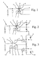
- a preamplifier as is known from the prior art is.
- Such a preamplifier is used to amplify signal voltages a signal source 1 high source impedance used, lead within the one designed as an operational amplifier 2 - here switched as a voltage follower Preamplifier through between a signal input 3 and a first supply voltage terminal 4 and a second supply voltage terminal 5 lying parasitic capacitances 6, 7 flowing leakage currents to a significant loss of signal.
- this is this as a voltage follower performed using the operational amplifier 2.
- the preamplifier in turn is operated by an operational amplifier connected as a voltage follower 2 formed, at the signal input 3, the signal voltage one Signal source 1 with high source impedance is present. Also with the one shown in FIG. 2 Operational amplifiers 2 are between the signal input 3 and the first supply voltage terminal 4 or the second supply voltage terminal 5 parasitic capacitances 6, 7 present. The negative influence of However, parasitic capacitances on the signal voltages are at least greatly reduced that the first and second supply voltage potential depend from the output signal of the preamplifier at signal output 8 in parallel are movable. This is a preamplifier in this embodiment thereby ensuring that the output signal is used directly as a reference potential for the supply voltage sources supplying the respective supply voltage potential 9, 10 serves.
- FIG. 3 of the drawing is another embodiment of a preamplifier shown, in which of an operational amplifier 2 and two resistors 11, 12 constructed preamplifiers determining the gain factor amplified the signal voltage. So despite this amplification of the output signal compared to the signal voltage, the leakage currents via the parasitic Capacities are prevented in the embodiment shown in FIG. 3 the respective supply voltage potential via a voltage divider 13, 14 from the output signal and the potential of a supply voltage source 15, 16 derivable.
- the signal output 8 of the operational amplifier 2 is not too heavy, is in that shown in Fig. 3 Embodiment between the center tap of the respective voltage divider 13, 14 and the associated supply voltage terminals 4, 5 each a voltage follower 17, 18 arranged.
- FIG. 4 of the drawing is another embodiment of a preamplifier shown, in which the first and second supply voltage potential directly shiftable depending on the attenuated output signal is. This is in the preamplifier shown in Fig. 4 by a before 2 switched supply voltage sources 9, 10 switched Attenuator 19 guaranteed.
- FIG. 5 shows a further exemplary embodiment of a preamplifier, in which the operational amplifier 2 in turn acts as a voltage follower is switched that the output signal of the operational amplifier present at the signal output 8 2 is amplified in an amplifier 20, however, the Supply voltage potentials of the operational amplifier 2 immediately the amplified output signal of the operational amplifier 2 in the manner of in Fig. 2 shown first embodiment can be derived.
- FIG. 6 of the drawing is an embodiment of a preamplifier shown according to the teaching of the invention, in which the output signal with With the help of a signal output 8 one connected as a voltage follower Operational amplifier 2 connected low-pass filter 21 is filtered. This filtered The output signal then serves as the basis for shifting the supply voltage potentials according to the type shown in Fig. 2.
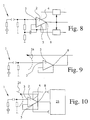
- the potential is one between the signal source 1 and the signal input 3 lying shield 24 of Signal source 1 controllable by the output signal of the preamplifier.
- FIG. 10 Another embodiment of a preamplifier is shown in FIG. 10.
- a parallel shift in the supply voltage potentials depending on the output signal according to one of the previously described exemplary embodiments, realized here with the help of a only shown schematically Shift circuit 25, and at the same time one between the signal source and the shield 24 located at the signal input to that at the signal output 8 applied potential raised.
- FIG. 11 of the drawing of a preamplifier in which the shield 24 in the area of Signal output 8 of the operational amplifier 2 is arranged.
- FIG. 12 the drawing of a further exemplary embodiment is a Pre-amplifier shown, in which the potential of the shield 24 indirectly from the output signal, for example from an amplified output signal is controllable. This depends on the external interference may be an advantage.
Landscapes
- Engineering & Computer Science (AREA)
- Power Engineering (AREA)
- Amplifiers (AREA)
Priority Applications (5)
| Application Number | Priority Date | Filing Date | Title |
|---|---|---|---|
| JP14488497A JP3261337B2 (ja) | 1997-06-03 | 1997-06-03 | 信号電圧増幅用前置増幅器 |
| US08/868,849 US6040741A (en) | 1997-06-03 | 1997-06-04 | Preamplifier for amplifying signal voltages from a signal source with high source impedance |
| DE59709698T DE59709698D1 (de) | 1997-06-03 | 1997-06-04 | Vorverstärker zur Verstärkung von Signalspannungen einer Signalquelle hoher Quellenimpedanz |
| DK97108965T DK0883239T3 (da) | 1997-06-03 | 1997-06-04 | Forforstærker til forstærkning af signalspændinger fra en signalkilde med høj kildeimpedans |
| EP97108965A EP0883239B1 (de) | 1997-06-03 | 1997-06-04 | Vorverstärker zur Verstärkung von Signalspannungen einer Signalquelle hoher Quellenimpedanz |
Applications Claiming Priority (3)
| Application Number | Priority Date | Filing Date | Title |
|---|---|---|---|
| JP14488497A JP3261337B2 (ja) | 1997-06-03 | 1997-06-03 | 信号電圧増幅用前置増幅器 |
| US08/868,849 US6040741A (en) | 1997-06-03 | 1997-06-04 | Preamplifier for amplifying signal voltages from a signal source with high source impedance |
| EP97108965A EP0883239B1 (de) | 1997-06-03 | 1997-06-04 | Vorverstärker zur Verstärkung von Signalspannungen einer Signalquelle hoher Quellenimpedanz |
Publications (2)
| Publication Number | Publication Date |
|---|---|
| EP0883239A1 EP0883239A1 (de) | 1998-12-09 |
| EP0883239B1 true EP0883239B1 (de) | 2003-04-02 |
Family
ID=27238227
Family Applications (1)
| Application Number | Title | Priority Date | Filing Date |
|---|---|---|---|
| EP97108965A Expired - Lifetime EP0883239B1 (de) | 1997-06-03 | 1997-06-04 | Vorverstärker zur Verstärkung von Signalspannungen einer Signalquelle hoher Quellenimpedanz |
Country Status (5)
| Country | Link |
|---|---|
| US (1) | US6040741A (da) |
| EP (1) | EP0883239B1 (da) |
| JP (1) | JP3261337B2 (da) |
| DE (1) | DE59709698D1 (da) |
| DK (1) | DK0883239T3 (da) |
Families Citing this family (3)
| Publication number | Priority date | Publication date | Assignee | Title |
|---|---|---|---|---|
| EP1219966A3 (de) * | 2000-11-04 | 2003-10-22 | ABB PATENT GmbH | Einrichtung zur Messung kleiner Spannungssignale |
| US7262663B2 (en) * | 2005-10-26 | 2007-08-28 | Agilent Technologies, Inc. | Ultra high linearity amplifier |
| PL222066B1 (pl) * | 2011-08-19 | 2016-06-30 | Akademia Górniczo Hutnicza Im Stanisława Staszica W Krakowie | Adaptacyjny dzielnik napięcia o skorygowanej charakterystyce częstotliwościowej do pomiaru wysokich napięć |
Family Cites Families (11)
| Publication number | Priority date | Publication date | Assignee | Title |
|---|---|---|---|---|
| DE134711C (da) * | ||||
| DE101789C (da) * | ||||
| US3521179A (en) * | 1968-04-02 | 1970-07-21 | Weston Instruments Inc | Amplifier with source voltage control |
| DE1918618A1 (de) * | 1969-04-12 | 1970-10-15 | Licentia Gmbh | Transistorwechselstromverstaerker mit einer Gegentaktendstufe |
| US3781672A (en) * | 1971-05-10 | 1973-12-25 | Drexelbrook Controls | Continuous condition measuring system |
| US3860882A (en) * | 1971-05-10 | 1975-01-14 | Drexelbrook Controls | Continuous condition measuring system |
| US4479093A (en) * | 1981-12-03 | 1984-10-23 | Inventab Audio Kb | Amplifier having high common mode rejection |
| FR2572604B1 (fr) * | 1984-10-31 | 1988-11-25 | Tacussel Jacques | Amplificateur de signaux continus et alternatifs a reponse en frequence etendue et a tension et courant de sortie eleves |
| US4751471A (en) * | 1985-08-21 | 1988-06-14 | Spring Creek Institute, Inc. | Amplifying circuit particularly adapted for amplifying a biopotential input signal |
| US4669479A (en) * | 1985-08-21 | 1987-06-02 | Spring Creek Institute, Inc. | Dry electrode system for detection of biopotentials |
| JPH0567932A (ja) * | 1990-12-27 | 1993-03-19 | Pioneer Electron Corp | 増幅器 |
-
1997
- 1997-06-03 JP JP14488497A patent/JP3261337B2/ja not_active Expired - Fee Related
- 1997-06-04 EP EP97108965A patent/EP0883239B1/de not_active Expired - Lifetime
- 1997-06-04 DE DE59709698T patent/DE59709698D1/de not_active Expired - Lifetime
- 1997-06-04 DK DK97108965T patent/DK0883239T3/da active
- 1997-06-04 US US08/868,849 patent/US6040741A/en not_active Expired - Lifetime
Also Published As
| Publication number | Publication date |
|---|---|
| US6040741A (en) | 2000-03-21 |
| EP0883239A1 (de) | 1998-12-09 |
| JP3261337B2 (ja) | 2002-02-25 |
| JPH1117458A (ja) | 1999-01-22 |
| DE59709698D1 (de) | 2003-05-08 |
| DK0883239T3 (da) | 2003-07-14 |
Similar Documents
| Publication | Publication Date | Title |
|---|---|---|
| DE2429953C3 (de) | Schaltungsanordnung zur Verarbeitung physiologischer Meßsignale | |
| DE69022108T2 (de) | Verstärkeranordnung. | |
| DE102004052174B4 (de) | Verstärkerschaltung, umfassend einen Verstärker mit tiefpassgefilterter Rückkopplung | |
| DE69505649T2 (de) | Verstärkerschaltung | |
| EP0007074A1 (de) | Verstärkeranordnung mit Störsignalunterdrückung | |
| EP0883239B1 (de) | Vorverstärker zur Verstärkung von Signalspannungen einer Signalquelle hoher Quellenimpedanz | |
| DE69118124T2 (de) | Schaltung für die Unterdrückung des durch das Schalten von zwei Spannungsquellen, hervorgerufen Geräusches, insbesondere für Audio-Vorverstärkerstufen | |
| DE2311379C3 (de) | Transistorverstärker für breitbandige Informationssignale | |
| DE60021433T2 (de) | Verfahren und Vorrichtung zur Steuerung der Gleichtaktimpedanzasymmetrie einer isolierten unsymmetrieschen Schaltung | |
| DE3310978C2 (de) | Verstärkerschaltung | |
| DE10031521B4 (de) | Integrierter Schaltkreis mit einem Analogverstärker | |
| DE3818142C2 (da) | ||
| DE19545387C2 (de) | Vorverstärker zur Verstärkung von Signalspannungen einer Signalquelle hoher Quellenimpedanz | |
| DE3855993T2 (de) | Schaltkreis zum Schalten der Leseköpfe eines Videorecorders | |
| DE2429954B2 (de) | Schaltungsanordnung zur Verarbeitung physiologischer Meßsignale | |
| DE3036917C2 (de) | Verstärkerschaltungsanordnung | |
| WO2003049282A1 (de) | Voll differentieller differenzverstärker mit hoher eingangsimpedanz | |
| DE3724980A1 (de) | Spannungswiederholerschaltung fuer eine ohmsche komponente aufweisende last mit kompensation der oberwellenverzerrung | |
| DE1190978B (de) | Schaltungsanordnung fuer eine Fernsehaufnahmeroehre vom Vidikontyp | |
| DE4311943B4 (de) | Schaltungsanordnung zum Begrenzen der Amplitude eines Nutzsignals | |
| DE3109441A1 (de) | Operationsverstaerker mit erhoehter einschwinggeschwindigkeit | |
| DE69816719T2 (de) | Verstärker | |
| EP0456321A2 (de) | Schaltungsanordnung mit elektronisch steuerbarem Übertragungsverhalten | |
| DE102020130812A1 (de) | Spannungsverstärker, Stromsensor mit derartigem Spannungsverstärker und Verfahren zur Inbetriebnahme eines derartigen Spannungsverstärkers | |
| EP1881599A1 (de) | Frequenzselektiver Transimpedanzverstärker |
Legal Events
| Date | Code | Title | Description |
|---|---|---|---|
| PUAI | Public reference made under article 153(3) epc to a published international application that has entered the european phase |
Free format text: ORIGINAL CODE: 0009012 |
|
| AK | Designated contracting states |
Kind code of ref document: A1 Designated state(s): CH DE DK FR GB LI NL |
|
| 17P | Request for examination filed |
Effective date: 19981130 |
|
| AKX | Designation fees paid |
Free format text: CH DE DK FR GB LI NL |
|
| 17Q | First examination report despatched |
Effective date: 20001121 |
|
| GRAH | Despatch of communication of intention to grant a patent |
Free format text: ORIGINAL CODE: EPIDOS IGRA |
|
| GRAH | Despatch of communication of intention to grant a patent |
Free format text: ORIGINAL CODE: EPIDOS IGRA |
|
| GRAA | (expected) grant |
Free format text: ORIGINAL CODE: 0009210 |
|
| AK | Designated contracting states |
Designated state(s): CH DE DK FR GB LI NL |
|
| REG | Reference to a national code |
Ref country code: GB Ref legal event code: FG4D Free format text: NOT ENGLISH |
|
| REG | Reference to a national code |
Ref country code: CH Ref legal event code: EP |
|
| REF | Corresponds to: |
Ref document number: 59709698 Country of ref document: DE Date of ref document: 20030508 Kind code of ref document: P |
|
| REG | Reference to a national code |
Ref country code: CH Ref legal event code: NV Representative=s name: KATZAROV S.A. |
|
| GBT | Gb: translation of ep patent filed (gb section 77(6)(a)/1977) | ||
| REG | Reference to a national code |
Ref country code: DK Ref legal event code: T3 |
|
| ET | Fr: translation filed | ||
| PLBE | No opposition filed within time limit |
Free format text: ORIGINAL CODE: 0009261 |
|
| STAA | Information on the status of an ep patent application or granted ep patent |
Free format text: STATUS: NO OPPOSITION FILED WITHIN TIME LIMIT |
|
| 26N | No opposition filed |
Effective date: 20040105 |
|
| PGFP | Annual fee paid to national office [announced via postgrant information from national office to epo] |
Ref country code: NL Payment date: 20050615 Year of fee payment: 9 |
|
| PG25 | Lapsed in a contracting state [announced via postgrant information from national office to epo] |
Ref country code: NL Free format text: LAPSE BECAUSE OF NON-PAYMENT OF DUE FEES Effective date: 20070101 |
|
| NLV4 | Nl: lapsed or anulled due to non-payment of the annual fee |
Effective date: 20070101 |
|
| PGFP | Annual fee paid to national office [announced via postgrant information from national office to epo] |
Ref country code: DK Payment date: 20120620 Year of fee payment: 16 Ref country code: CH Payment date: 20120622 Year of fee payment: 16 |
|
| PGFP | Annual fee paid to national office [announced via postgrant information from national office to epo] |
Ref country code: GB Payment date: 20120622 Year of fee payment: 16 Ref country code: FR Payment date: 20120705 Year of fee payment: 16 |
|
| PGFP | Annual fee paid to national office [announced via postgrant information from national office to epo] |
Ref country code: DE Payment date: 20120830 Year of fee payment: 16 |
|
| REG | Reference to a national code |
Ref country code: CH Ref legal event code: PL |
|
| REG | Reference to a national code |
Ref country code: DK Ref legal event code: EBP Effective date: 20130630 |
|
| GBPC | Gb: european patent ceased through non-payment of renewal fee |
Effective date: 20130604 |
|
| REG | Reference to a national code |
Ref country code: DE Ref legal event code: R119 Ref document number: 59709698 Country of ref document: DE Effective date: 20140101 |
|
| REG | Reference to a national code |
Ref country code: FR Ref legal event code: ST Effective date: 20140228 |
|
| PG25 | Lapsed in a contracting state [announced via postgrant information from national office to epo] |
Ref country code: CH Free format text: LAPSE BECAUSE OF NON-PAYMENT OF DUE FEES Effective date: 20130630 Ref country code: DE Free format text: LAPSE BECAUSE OF NON-PAYMENT OF DUE FEES Effective date: 20140101 Ref country code: LI Free format text: LAPSE BECAUSE OF NON-PAYMENT OF DUE FEES Effective date: 20130630 Ref country code: GB Free format text: LAPSE BECAUSE OF NON-PAYMENT OF DUE FEES Effective date: 20130604 |
|
| PG25 | Lapsed in a contracting state [announced via postgrant information from national office to epo] |
Ref country code: FR Free format text: LAPSE BECAUSE OF NON-PAYMENT OF DUE FEES Effective date: 20130701 |
|
| PG25 | Lapsed in a contracting state [announced via postgrant information from national office to epo] |
Ref country code: DK Free format text: LAPSE BECAUSE OF NON-PAYMENT OF DUE FEES Effective date: 20130630 |