EP0883239B1 - Preamplifier for amplifying signal voltages of a signal source with high source impedance - Google Patents
Preamplifier for amplifying signal voltages of a signal source with high source impedance Download PDFInfo
- Publication number
- EP0883239B1 EP0883239B1 EP97108965A EP97108965A EP0883239B1 EP 0883239 B1 EP0883239 B1 EP 0883239B1 EP 97108965 A EP97108965 A EP 97108965A EP 97108965 A EP97108965 A EP 97108965A EP 0883239 B1 EP0883239 B1 EP 0883239B1
- Authority
- EP
- European Patent Office
- Prior art keywords
- signal
- preamplifier
- supply voltage
- source
- output signal
- Prior art date
- Legal status (The legal status is an assumption and is not a legal conclusion. Google has not performed a legal analysis and makes no representation as to the accuracy of the status listed.)
- Expired - Lifetime
Links
Images


Classifications
-
- H—ELECTRICITY
- H03—ELECTRONIC CIRCUITRY
- H03F—AMPLIFIERS
- H03F1/00—Details of amplifiers with only discharge tubes, only semiconductor devices or only unspecified devices as amplifying elements
- H03F1/02—Modifications of amplifiers to raise the efficiency, e.g. gliding Class A stages, use of an auxiliary oscillation
- H03F1/0205—Modifications of amplifiers to raise the efficiency, e.g. gliding Class A stages, use of an auxiliary oscillation in transistor amplifiers
- H03F1/0211—Modifications of amplifiers to raise the efficiency, e.g. gliding Class A stages, use of an auxiliary oscillation in transistor amplifiers with control of the supply voltage or current
- H03F1/0216—Continuous control
- H03F1/0233—Continuous control by using a signal derived from the output signal, e.g. bootstrapping the voltage supply
-
- H—ELECTRICITY
- H03—ELECTRONIC CIRCUITRY
- H03F—AMPLIFIERS
- H03F3/00—Amplifiers with only discharge tubes or only semiconductor devices as amplifying elements
- H03F3/45—Differential amplifiers
- H03F3/45071—Differential amplifiers with semiconductor devices only
- H03F3/45479—Differential amplifiers with semiconductor devices only characterised by the way of common mode signal rejection
- H03F3/45928—Differential amplifiers with semiconductor devices only characterised by the way of common mode signal rejection using IC blocks as the active amplifying circuit
- H03F3/45932—Differential amplifiers with semiconductor devices only characterised by the way of common mode signal rejection using IC blocks as the active amplifying circuit by using feedback means
-
- H—ELECTRICITY
- H03—ELECTRONIC CIRCUITRY
- H03F—AMPLIFIERS
- H03F2200/00—Indexing scheme relating to amplifiers
- H03F2200/504—Indexing scheme relating to amplifiers the supply voltage or current being continuously controlled by a controlling signal, e.g. the controlling signal of a transistor implemented as variable resistor in a supply path for, an IC-block showed amplifier
Definitions
- the invention relates to a preamplifier for amplifying signal voltages a signal source of high source impedance with one with the signal source connected signal input, with a first with a first supply voltage potential connected supply voltage terminal, with a second second connected to a second supply voltage potential Supply voltage terminal and with an output signal supplying Signal output.
- preamplifiers are designed for the prior art the most diverse areas of application.
- a particular problem with Use of preamplifiers occurs in cases where the one to be amplified Signal voltage from a signal source with high or very high source impedance comes.
- the invention is therefore based on the object of an improvement indicate the susceptibility of the preamplifier to interference.
- the object presented and set forth above is solved in that with the signal output a low-pass filter for filtering of the output signal is connected and the first and second supply voltage potential can be moved in parallel depending on the low-pass filtered output signal are.
- the high signal losses for example when amplifying a signal voltage of a signal source higher Source impedance using an operational amplifier connected as a voltage follower occur, are essentially due to the fact that leakage currents about the parasitic capacitances between the signal input of the operational amplifier and the first and second in the prior art at constant Potential supply voltage terminal of the operational amplifier flow away. These leakage currents occur in other known preamplifiers the same way on.
- the preamplifier according to the teaching of the invention experiences a first advantageous one Design in that it is designed as a voltage follower. At a Such design of the preamplifier ensures that the shift the supply voltage potentials depending on the output signal even if the aim is to completely eliminate the influences of the parasitic Capacity is particularly easy to ensure.
- the preamplifier according to the teaching of the invention Signal voltage amplified, this generally results in a more difficult implementation the shift of the supply voltage potentials depending on the low-pass filtered output signal under the condition of reduced leakage currents, at the same time, however, an actual one is already in the pre-amplification stage Guaranteed increase in signal level without signal loss.
- the preamplifier according to the teaching of the invention so that first and second supply voltage potential directly dependent on the attenuated output signal can be shifted, for example in the case of a weakening to 95%, the complete elimination of the parasitic capacities, however, is usually an increase in the stability of the Preamplifier guaranteed.
- the preamplifier is designed as a voltage follower according to the teaching of the invention, it is particularly advantageous to design the preamplifier so that that the output signal directly as a reference potential for the particular Supply voltage sources supplying supply voltage potential serves. This is a particularly simple shift in the supply voltage potentials thus ensures that the leakage currents over the parasitic capacitances of the preamplifier are eliminated.
- the preamplifier where the signal voltage is amplified at the same time, it is special advantageous to design the preamplifier in that the respective supply voltage potential via a voltage divider from the output signal and the potential a supply voltage source can be derived.
- the respective supply voltage potential via a voltage divider from the output signal and the potential a supply voltage source can be derived.
- the voltage divider can thus also from an amplified output signal the respective supply voltage potential is tracked in such a way that the disruptive influence of parasitic capacitances at least largely is eliminated.
- the preamplifier according to the first is particularly easy to implement Teaching of the invention in that it is designed as an operational amplifier is. In the case of an operational amplifier, the influence on the Supply voltage potentials simple and with little repercussions the output signal connected.
- the potential a shielding of the signal source is controllable from the output signal.
- This configuration of the preamplifier ensures that external Interference fields or parasitic capacitances between the signal source on the one hand and environment due to the low source impedance of the Output signal of the preamplifier no or almost no influence on the Can take signal voltages of the signal source with high source impedance.
- the shield between the signal source and the Signal input arranged. This arrangement ensures that also the supply voltage potentials of the preamplifier have no influence on the Can take signal voltages.
- the shielding in the area of the signal output of the Preamplifier arranged so that a shielding of the signal source down to to the signal input is guaranteed.
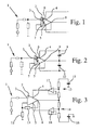
- a preamplifier as is known from the prior art is.
- Such a preamplifier is used to amplify signal voltages a signal source 1 high source impedance used, lead within the one designed as an operational amplifier 2 - here switched as a voltage follower Preamplifier through between a signal input 3 and a first supply voltage terminal 4 and a second supply voltage terminal 5 lying parasitic capacitances 6, 7 flowing leakage currents to a significant loss of signal.
- this is this as a voltage follower performed using the operational amplifier 2.
- the preamplifier in turn is operated by an operational amplifier connected as a voltage follower 2 formed, at the signal input 3, the signal voltage one Signal source 1 with high source impedance is present. Also with the one shown in FIG. 2 Operational amplifiers 2 are between the signal input 3 and the first supply voltage terminal 4 or the second supply voltage terminal 5 parasitic capacitances 6, 7 present. The negative influence of However, parasitic capacitances on the signal voltages are at least greatly reduced that the first and second supply voltage potential depend from the output signal of the preamplifier at signal output 8 in parallel are movable. This is a preamplifier in this embodiment thereby ensuring that the output signal is used directly as a reference potential for the supply voltage sources supplying the respective supply voltage potential 9, 10 serves.
- FIG. 3 of the drawing is another embodiment of a preamplifier shown, in which of an operational amplifier 2 and two resistors 11, 12 constructed preamplifiers determining the gain factor amplified the signal voltage. So despite this amplification of the output signal compared to the signal voltage, the leakage currents via the parasitic Capacities are prevented in the embodiment shown in FIG. 3 the respective supply voltage potential via a voltage divider 13, 14 from the output signal and the potential of a supply voltage source 15, 16 derivable.
- the signal output 8 of the operational amplifier 2 is not too heavy, is in that shown in Fig. 3 Embodiment between the center tap of the respective voltage divider 13, 14 and the associated supply voltage terminals 4, 5 each a voltage follower 17, 18 arranged.
- FIG. 4 of the drawing is another embodiment of a preamplifier shown, in which the first and second supply voltage potential directly shiftable depending on the attenuated output signal is. This is in the preamplifier shown in Fig. 4 by a before 2 switched supply voltage sources 9, 10 switched Attenuator 19 guaranteed.
- FIG. 5 shows a further exemplary embodiment of a preamplifier, in which the operational amplifier 2 in turn acts as a voltage follower is switched that the output signal of the operational amplifier present at the signal output 8 2 is amplified in an amplifier 20, however, the Supply voltage potentials of the operational amplifier 2 immediately the amplified output signal of the operational amplifier 2 in the manner of in Fig. 2 shown first embodiment can be derived.
- FIG. 6 of the drawing is an embodiment of a preamplifier shown according to the teaching of the invention, in which the output signal with With the help of a signal output 8 one connected as a voltage follower Operational amplifier 2 connected low-pass filter 21 is filtered. This filtered The output signal then serves as the basis for shifting the supply voltage potentials according to the type shown in Fig. 2.
- the potential is one between the signal source 1 and the signal input 3 lying shield 24 of Signal source 1 controllable by the output signal of the preamplifier.
- FIG. 10 Another embodiment of a preamplifier is shown in FIG. 10.
- a parallel shift in the supply voltage potentials depending on the output signal according to one of the previously described exemplary embodiments, realized here with the help of a only shown schematically Shift circuit 25, and at the same time one between the signal source and the shield 24 located at the signal input to that at the signal output 8 applied potential raised.
- FIG. 11 of the drawing of a preamplifier in which the shield 24 in the area of Signal output 8 of the operational amplifier 2 is arranged.
- FIG. 12 the drawing of a further exemplary embodiment is a Pre-amplifier shown, in which the potential of the shield 24 indirectly from the output signal, for example from an amplified output signal is controllable. This depends on the external interference may be an advantage.
Description
Die Erfindung betrifft einen Vorverstärker zur Verstärkung von Signalspannungen einer Signalquelle hoher Quellenimpedanz mit einem mit der Signalquelle verbundenen Signaleingang, mit einer ersten mit einem ersten Versorgungsspannungspotential verbundenen Versorgungsspannungsklemme, mit einer zweiten mit einem zweiten Versorgungsspannungspotential verbundenen zweiten Versorgungsspannungsklemme und mit einem ein Ausgangssignal liefernden Signalausgang.The invention relates to a preamplifier for amplifying signal voltages a signal source of high source impedance with one with the signal source connected signal input, with a first with a first supply voltage potential connected supply voltage terminal, with a second second connected to a second supply voltage potential Supply voltage terminal and with an output signal supplying Signal output.
Vorverstärker sind aus dem Stand der Technik in großer Anzahl, ausgebildet für die unterschiedlichsten Einsatzbereiche, bekannt. Ein besonderes Problem beim Einsatz von Vorverstärkern tritt in den Fällen auf, in denen die zu verstärkende Signalspannung aus einer Signalquelle mit hoher oder sehr hoher Quellenimpedanz stammt. Man kann beispielsweise feststellen, daß bei der Übertragung relativ niederfrequenter Signale über eine niedrige Koppelkapazität bei herkömmlichen, häufig als Vorverstärker eingesetzten, als Spannungsfolger geschalteten Operationsverstärkern mit hohem Ableitwiderstand schon hohe Signalverluste auftreten. Diese Signalverluste sind selbstverständlich unerwünscht.A large number of preamplifiers are designed for the prior art the most diverse areas of application. A particular problem with Use of preamplifiers occurs in cases where the one to be amplified Signal voltage from a signal source with high or very high source impedance comes. One can find, for example, that the transmission is relative low-frequency signals via a low coupling capacity in conventional, often used as a preamplifier, switched as a voltage follower Operational amplifiers with high leakage resistance already have high signal losses occur. These signal losses are of course undesirable.
Beim Einsatz von Vorverstärkern zur Verstärkung von Signalspannungen einer Signalquelle hoher Quellenimpedanz ist es bekanntermaßen problematisch, daß die Signalspannung aufgrund der hohen bis sehr hohen Quellenimpedanz sehr empfindlich gegenüber äußeren elektrischen Feldern ist. Solche äußeren elektrischen Felder können zu hohen Signalverlusten bereits vor dem Vorverstärker führen.When using preamplifiers to amplify signal voltages Signal source of high source impedance is known to be problematic in that the signal voltage due to the high to very high source impedance is sensitive to external electrical fields. Such external electrical Fields can cause high signal losses even before the preamplifier to lead.
Aus der US 3,521,179, die einen eingangs beschriebenen, gattungsgemäßen Vorverstärker zeigt, ist es bekannt, daß das erste Versorgungsspannungspotential sowie das zweite Versorgungsspannungspotential abhängig von dem Ausgangssignal parallel verschiebbar sind. Eine wesentliche Verbesserung der Störungsanfälligkeit des Vorverstärkers wird damit jedoch nicht erzielt.From US 3,521,179, the generic described above Preamplifier shows, it is known that the first supply voltage potential and the second supply voltage potential depending on the output signal can be moved in parallel. A significant improvement in susceptibility to failure the preamplifier is not achieved.
Der Erfindung liegt somit die Aufgabe zugrunde, eine Verbesserung bezüglich der Störungsanfälligkeit des Vorverstärkers anzugeben. The invention is therefore based on the object of an improvement indicate the susceptibility of the preamplifier to interference.
Gemäß der Lehre der Erfindung ist die zuvor aufgezeigte und dargelegte Aufgabe dadurch gelöst, daß mit dem Signalausgang ein Tiefpaßfilter zum Filtern des Ausgangssignals verbunden ist und das erste und zweite Versorgungsspannungspotential abhängig von dem tiefpaßgefilterten Ausgangssignal parallel verschiebbar sind.In accordance with the teachings of the invention, the object presented and set forth above is solved in that with the signal output a low-pass filter for filtering of the output signal is connected and the first and second supply voltage potential can be moved in parallel depending on the low-pass filtered output signal are.
Erfindungsgemäß ist erkannt worden, daß die hohen Signalverluste, die beispielsweise bei der Verstärkung einer Signalspannung einer Signalquelle hoher Quellenimpedanz mit Hilfe eines als Spannungsfolger geschalteten Operationsverstärkers auftreten, im wesentlichen darin begründet sind, daß Verlustströme über die parasitären Kapazitäten zwischen dem Signaleingang des Operationsverstärkers und der ersten bzw. zweiten im Stand der Technik auf konstantem Potential liegenden Versorgungsspannungsklemme des Operationsverstärkers abfließen. Diese Verlustströme treten bei anderen bekannten Vorverstärkern in der gleichen Art und Weise auf.According to the invention it has been recognized that the high signal losses, for example when amplifying a signal voltage of a signal source higher Source impedance using an operational amplifier connected as a voltage follower occur, are essentially due to the fact that leakage currents about the parasitic capacitances between the signal input of the operational amplifier and the first and second in the prior art at constant Potential supply voltage terminal of the operational amplifier flow away. These leakage currents occur in other known preamplifiers the same way on.
Durch die erfindungsgemäße Kopplung des ersten und zweiten Versorgungsspannungspotentials an das tiefpaßgefilterte Ausgangssignal des Vorverstärkers wird erreicht, daß die Verlustströme über die parasitären Kapazitäten - aufgrund der nur noch reduziert oder überhaupt nicht mehr schwankenden Potentialdifferenzen an den parasitären Kapazitäten - zumindest reduzierbar, wenn nicht vollständig eliminierbar sind.By coupling the first and second supply voltage potentials according to the invention to the low-pass filtered output signal of the preamplifier is achieved that the leakage currents on the parasitic capacitances - due the only reduced or no longer fluctuating potential differences on the parasitic capacitances - at least reducible, if not complete can be eliminated.
Praktische Versuche haben gezeigt, daß z. B. bei einer 25 Hz-Signalquelle mit einem in Reihe geschalteten Kondensator einer Kapazität von 10 pF als Quellenimpedanz bei herkömmlichen Vorverstärkern ein Signalverlust von ungefähr 20 % auftritt. Die erfindungsgemäße Verschiebung des ersten und zweiten Versorgungsspannungspotentials abhängig von dem Ausgangssignal des Vorverstärkers führte bei derselben Signalquelle zu einer Reduzierung des Signalverlustes bei der Übertragung auf weniger als 0,01 %.Practical tests have shown that e.g. B. with a 25 Hz signal source a series capacitor with a capacitance of 10 pF as source impedance with conventional preamplifiers, a signal loss of approximately 20% occurs. The displacement of the first and second supply voltage potentials according to the invention depending on the output signal of the preamplifier led to a reduction in signal loss for the same signal source when transferring to less than 0.01%.
Der Vorverstärker gemäß der Lehre der Erfindung erfährt eine erste vorteilhafte Ausgestaltung dadurch, daß er als Spannungsfolger ausgebildet ist. Bei einer derartigen Ausgestaltung des Vorverstärkers ist gewährleistet, daß die Verschiebung der Versorgungsspannungspotentiale abhängig von dem Ausgangssignal auch bei einer angestrebten völligen Eliminierung der Einflüsse der parasitären Kapazitäten besonders einfach zu gewährleisten ist. The preamplifier according to the teaching of the invention experiences a first advantageous one Design in that it is designed as a voltage follower. At a Such design of the preamplifier ensures that the shift the supply voltage potentials depending on the output signal even if the aim is to completely eliminate the influences of the parasitic Capacity is particularly easy to ensure.
Dadurch, daß alternativ der Vorverstärker gemäß der Lehre der Erfindung die Signalspannung verstärkt, ergibt sich zwar in der Regel eine schwierigere Realisierung der Verschiebung der Versorgungsspannungspotentiale abhängig von dem tiefpaßgefilterten Ausgangssignal unter der Bedingung reduzierter Verlustströme, gleichzeitig ist jedoch schon in der Vorverstärkungsstufe eine tatsächliche Erhöhung des Signalpegels ohne Signalverluste gewährleistet.In that, alternatively, the preamplifier according to the teaching of the invention Signal voltage amplified, this generally results in a more difficult implementation the shift of the supply voltage potentials depending on the low-pass filtered output signal under the condition of reduced leakage currents, at the same time, however, an actual one is already in the pre-amplification stage Guaranteed increase in signal level without signal loss.
Legt man nun den Vorverstärker gemäß der Lehre der Erfindung so aus, daß das erste und zweite Versorgungsspannungspotential unmittelbar abhängig von dem abgeschwächten Ausgangssignal verschiebbar ist, erreicht man zwar beispielsweise bei einer Abschwächung auf 95 % keine vollständige Eliminierung der parasitären Kapazitäten, jedoch ist in der Regel eine Erhöhung der Stabilität des Vorverstärkers gewährleistet.If one designs the preamplifier according to the teaching of the invention so that first and second supply voltage potential directly dependent on the attenuated output signal can be shifted, for example in the case of a weakening to 95%, the complete elimination of the parasitic capacities, however, is usually an increase in the stability of the Preamplifier guaranteed.
Ist der Vorverstärker gemäß der Lehre der Erfindung als Spannungsfolger ausgebildet, so ist es besonders vorteilhaft, den Vorverstärker dadurch auszugestalten, daß das Ausgangssignal unmittelbar als Bezugspotential für die das jeweilige Versorgungsspannungspotential liefernden Versorgungsspannungsquellen dient. Hierdurch ist eine besonders einfache Verschiebung der Versorgungsspannungspotentiale so gewährleistet, daß die Verlustströme über die parasitären Kapazitäten des Vorverstärkers eliminiert sind.If the preamplifier is designed as a voltage follower according to the teaching of the invention, it is particularly advantageous to design the preamplifier so that that the output signal directly as a reference potential for the particular Supply voltage sources supplying supply voltage potential serves. This is a particularly simple shift in the supply voltage potentials thus ensures that the leakage currents over the parasitic capacitances of the preamplifier are eliminated.
Insbesondere bei der Variante des Vorverstärkers gemäß der Lehre der Erfindung, bei der die Signalspannung gleichzeitig verstärkt wird, ist es besonders vorteilhaft, den Vorverstärker dadurch auszugestalten, daß das jeweilige Versorgungsspannungspotential über einen Spannungsteiler aus dem Ausgangssignal und dem Potential jeweils einer Versorgungsspannungsquelle ableitbar ist. Durch entsprechende Wahl des Spannungsteilers kann somit auch aus einem verstärkten Ausgangssignal das jeweilige Versorgungsspannungspotential so nachgeführt werden, daß der störende Einfluß der parasitären Kapazitäten zumindest weitgehend eliminiert ist.In particular in the variant of the preamplifier according to the teaching of the invention, where the signal voltage is amplified at the same time, it is special advantageous to design the preamplifier in that the respective supply voltage potential via a voltage divider from the output signal and the potential a supply voltage source can be derived. By appropriate Choice of the voltage divider can thus also from an amplified output signal the respective supply voltage potential is tracked in such a way that the disruptive influence of parasitic capacitances at least largely is eliminated.
Besonders einfach gelingt die Realisierung des Vorverstärkers gemäß der ersten Lehre der Erfindung dadurch, daß dieser als Operationsverstärker ausgebildet ist. Bei einem Operationsverstärker ist insbesondere die Einflußnahme auf die Versorgungsspannungspotentiale einfach und mit geringen Rückwirkungen auf das Ausgangssignal verbunden.The preamplifier according to the first is particularly easy to implement Teaching of the invention in that it is designed as an operational amplifier is. In the case of an operational amplifier, the influence on the Supply voltage potentials simple and with little repercussions the output signal connected.
Gemäß einer bevorzugten Weiterbildung ist ferner vorgesehen, daß das Potential einer Abschirmung der Signalquelle von dem Ausgangssignal steuerbar ist. Durch diese Ausgestaltung des Vorverstärkers ist gewährleistet, daß äußere Störfelder bzw. parasitäre Kapazitäten zwischen der Signalquelle einerseits und der Umgebung andererseits aufgrund der geringen Quellenimpedanz des Ausgangssignals des Vorverstärkers keinen bzw. nahezu keinen Einfluß auf die Signalspannungen der Signalquelle mit hoher Quellenimpedanz nehmen können.According to a preferred development, it is further provided that the potential a shielding of the signal source is controllable from the output signal. This configuration of the preamplifier ensures that external Interference fields or parasitic capacitances between the signal source on the one hand and environment due to the low source impedance of the Output signal of the preamplifier no or almost no influence on the Can take signal voltages of the signal source with high source impedance.
Gemäß einer ersten alternativen Ausgestaltung des Vorverstärkers nach der Lehre der Erfindung ist die Abschirmung zwischen der Signalquelle und dem Signaleingang angeordnet. Durch diese Anordnung ist gewährleistet, daß auch die Versorgungsspannungspotentiale des Vorverstärkers keinen Einfluß auf die Signalspannungen nehmen können.According to a first alternative embodiment of the preamplifier according to the Teaching of the invention is the shield between the signal source and the Signal input arranged. This arrangement ensures that also the supply voltage potentials of the preamplifier have no influence on the Can take signal voltages.
Gemäß einer zweiten alternativen Ausgestaltung des Vorverstärkers nach der Lehre der Erfindung ist die Abschirmung im Bereich des Signalausgangs des Vorverstärkers angeordnet, so daß eine Abschirmung der Signalquelle bis hin zum Signaleingang gewährleistet ist.According to a second alternative embodiment of the preamplifier according to the The teaching of the invention is the shielding in the area of the signal output of the Preamplifier arranged so that a shielding of the signal source down to to the signal input is guaranteed.
Im einzelnen gibt es nun eine Vielzahl von Möglichkeiten, den erfindungsgemäßen Vorverstärker zur Verstärkung von Signalspannungen einer Signalquelle hoher Quellenimpedanz auszugestalten und weiterzubilden. Dazu wird verwiesen einerseits auf die dem Patentanspruch 1 nachgeordneten Patentansprüche, andererseits auf die Beschreibung von bevorzugten Ausführungsbeispielen in Verbindung mit der Zeichnung. In der Zeichnung zeigt
- Fig. 1
- ein Ausführungsbeispiel eines aus dem Stand der Technik bekannten Vorverstärkers,
- Fig. 2
- ein weiteres Ausführungsbeispiel eines Vorverstärkers,
- Fig. 3
- ein weiteres Ausführungsbeispiel eines Vorverstärkers,
- Fig. 4
- ein weiteres Ausführungsbeispiel eines Vorverstärkers,
- Fig. 5
- ein weiteres Ausführungsbeispiel eines Vorverstärkers,
- Fig. 6
- ein Ausführungsbeispiel eines Vorverstärkers gemäß der Lehre der Erfindung,
- Fig. 7
- ein weiteres Ausführungsbeispiel eines Vorverstärkers,
- Fig. 8
- ein weiteres Ausführungsbeispiel eines Vorverstärkers,
- Fig. 9
- ein weiteres Ausführungsbeispiel eines Vorverstärkers,
- Fig. 10
- ein weiteres Ausführungsbeispiel eines Vorverstärkers,
- Fig. 11
- ein weiteres Ausführungsbeispiel eines Vorverstärkers und
- Fig. 12
- ein weiteres Ausführungsbeispiel eines Vorverstärkers.
- Fig. 1
- an embodiment of a preamplifier known from the prior art,
- Fig. 2
- another embodiment of a preamplifier,
- Fig. 3
- another embodiment of a preamplifier,
- Fig. 4
- another embodiment of a preamplifier,
- Fig. 5
- another embodiment of a preamplifier,
- Fig. 6
- an embodiment of a preamplifier according to the teaching of the invention,
- Fig. 7
- another embodiment of a preamplifier,
- Fig. 8
- another embodiment of a preamplifier,
- Fig. 9
- another embodiment of a preamplifier,
- Fig. 10
- another embodiment of a preamplifier,
- Fig. 11
- another embodiment of a preamplifier and
- Fig. 12
- another embodiment of a preamplifier.
In Fig. 1 ist ein Vorverstärker gezeigt, wie er aus dem Stand der Technik bekannt
ist. Wird ein solcher Vorverstärker zur Verstärkung von Signalspannungen
einer Signalquelle 1 hoher Quellenimpedanz eingesetzt, so führen die innerhalb
des als Operationsverstärker 2 - hier als Spannungsfolger geschaltet-ausgebildeten
Vorverstärkers durch die zwischen einem Signaleingang 3 und
einer ersten Versorgungsspannungsklemme 4 und einer zweiten Versorgungsspannungsklemme
5 liegenden parasitären Kapazitäten 6, 7 fließenden Verlustströme
zu einem erheblichen Signalverlust. In dem Ausführungsbeispiel eines
aus dem Stand der Technik bekannten Vorverstärkers ist dieser als Spannungsfolger
unter Verwendung des Operationsverstärkers 2 ausgeführt.1 shows a preamplifier as is known from the prior art
is. Such a preamplifier is used to amplify signal voltages
a
In den folgenden Figuren sind die jeweils mit Fig. 1 übereinstimmenden Bauelemente mit den selben Bezugszeichen versehen.In the following figures, the components that correspond to FIG. 1 are shown provided with the same reference numerals.
Bei dem in Fig. 2 dargestellten Ausführungsbeispiel eines Vorverstärkers wird
der Vorverstärker wiederum von einem als Spannungsfolger geschalteten Operationsverstärker
2 gebildet, an dessen Signaleingang 3 die Signalspannung einer
Signalquelle 1 mit hoher Quellenimpedanz anliegt. Auch bei dem in Fig. 2 dargestellten
Operationsverstärker 2 sind zwischen dem Signaleingang 3 und der
ersten Versorgungsspannungsklemme 4 bzw. der zweiten Versorgungsspannungsklemme
5 parasitäre Kapazitäten 6, 7 vorhanden. Der negative Einfluß der
parasitären Kapazitäten auf die Signalspannungen ist jedoch dadurch zumindest
stark reduziert, daß das erste und zweite Versorgungsspannungspotential abhängig
von dem Ausgangssignal des Vorverstärkers am Signalausgang 8 parallel
verschiebbar sind. Dies ist bei diesem Ausführungsbeispiel eines Vorverstärkers
dadurch gewährleistet, daß das Ausgangssignal unmittelbar als Bezugspotential
für die das jeweilige Versorgungsspannungspotential liefernden Versorgungsspannungsquellen
9, 10 dient. In the embodiment of a preamplifier shown in FIG
the preamplifier in turn is operated by an operational amplifier connected as a
In Fig. 3 der Zeichnung ist ein weiteres Ausführungsbeispiel eines Vorverstärkers
dargestellt, bei welchem der aus einem Operationsverstärker 2 und zwei
den Verstärkungsfaktor bestimmenden Widerständen 11, 12 aufgebaute Vorverstärker
die Signalspannung verstärkt. Damit trotz dieser Verstärkung des Ausgangssignals
gegenüber der Signalspannung die Verlustströme über die parasitären
Kapazitäten verhindert werden, ist bei dem in Fig. 3 dargestellten Ausführungsbeispiel
das jeweilige Versorgungsspannungspotential über einen Spannungsteiler
13, 14 aus dem Ausgangssignal und dem Potential jeweils einer Versorgungsspannungsquelle
15, 16 ableitbar. Um den Signalausgang 8 des Operationsverstärkers
2 nicht zu stark zu belasten, ist bei dem in Fig. 3 dargestellten
Ausführungsbeispiel zwischen dem Mittelabgriff des jeweiligen Spannungsteilers
13, 14 und den zugehörigen Versorgungsspannungsklemmen 4, 5 jeweils
ein Spannungsfolger 17, 18 angeordnet.3 of the drawing is another embodiment of a preamplifier
shown, in which of an
In Fig. 4 der Zeichnung ist ein weiteres Ausführungsbeispiel eines Vorverstärkers
dargestellt, bei dem das erste und zweite Versorgungsspannungspotential
unmittelbar abhängig von dem abgeschwächten Ausgangssignal verschiebbar
ist. Dies wird bei dem in Fig. 4 dargestellten Vorverstärker durch einen vor die
nach Art der Fig. 2 geschalteten Versorgungsspannungsquellen 9, 10 geschalteten
Abschwächer 19 gewährleistet.4 of the drawing is another embodiment of a preamplifier
shown, in which the first and second supply voltage potential
directly shiftable depending on the attenuated output signal
is. This is in the preamplifier shown in Fig. 4 by a before
2 switched
Im Gegensatz dazu zeigt Fig. 5 ein weiteres Ausführungsbeispiel eines Vorverstärkers,
bei dem zwar der Operationsverstärker 2 wiederum als Spannungsfolger
geschaltet ist, daß am Signalausgang 8 anliegende Ausgangssignal des Operationsverstärkers
2 jedoch in einem Verstärker 20 verstärkt wird, wobei die
Versorgungsspannungspotentiale des Operationsverstärkers 2 unmittelbar aus
dem verstärkten Ausgangssignal des Operationsverstärkers 2 nach Art des in
Fig. 2 dargestellten ersten Ausführungsbeispiels abgeleitet werden.In contrast, FIG. 5 shows a further exemplary embodiment of a preamplifier,
in which the
In Fig. 6 der Zeichnung ist weiter ein Ausführungsbeispiel eines Vorverstärkers
nach der Lehre der Erfindung dargestellt, bei welchem das Ausgangssignal mit
Hilfe eines mit dem Signalausgang 8 eines als Spannungsfolger geschalteten
Operationsverstärkers 2 verbundenen Tiefpaßfilter 21 gefiltert wird. Dieses gefilterte
Ausgangssignal dient anschließend als Grundlage der Verschiebung der Versorgungsspannungspotentiale
nach der in Fig. 2 dargestellten Art.6 of the drawing is an embodiment of a preamplifier
shown according to the teaching of the invention, in which the output signal with
With the help of a
Um das bei den in Fig. 6 dargestellten Ausführungsbeispiel auftretende Problem
zu vermeiden, daß das Ausgangssignal auch zur Weiterverarbeitung nur mehr
durch den Tiefpaßfilter 21 gefiltert vorliegt, sind bei dem in Fig. 7 dargestellten
Ausführungsbeispiel nach der Lehre der Erfindung jeweils zwischen den
Versorgungsspannungsquellen 9, 10 und den Versorgungsspannungsklemmen 4,
5 zwei separate Tiefpaßfilter 22, 23 angeordnet.The problem that arises in the embodiment shown in FIG. 6
to avoid that the output signal only for further processing
is filtered by the low-
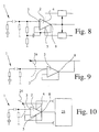
Bei dem in Fig. 8 dargestellten Ausführungsbeispiel weitere bekannte Maßnahmen getroffen, um die Eingangsimpedanz des Vorverstärkers zu erhöhen.In the exemplary embodiment shown in FIG. 8, further known measures hit to increase the input impedance of the preamplifier.
In Fig. 9 der Zeichnung ist nun ein weiteres Ausführungsbeispiel eines Vorverstärkers
dargestellt. Bei diesem Vorverstärker ist das Potential einer zwischen
der Signalquelle 1 und dem Signaleingang 3 liegenden Abschirmung 24 der
Signalquelle 1 von dem Ausgangssignal des Vorverstärkers steuerbar.9 of the drawing is another embodiment of a preamplifier
shown. With this preamplifier, the potential is one between
the
Ein weiteres Ausführungsbeispiel eines Vorverstärkers ist in Fig. 10 dargestellt.
Hier erfolgt eine parallele Verschiebung der Versorgungsspannungspotentiale
abhängig von dem Ausgangssignal nach einem der zuvor beschriebenen Ausführungsbeispiele,
hier verwirklicht mit Hilfe einer nur schematisch dargestellte
Verschiebeschaltung 25, und gleichzeitig wird eine zwischen der Signalquelle
und dem Signaleingang liegende Abschirmung 24 auf das am Signalausgang 8
anliegende Potential angehoben.Another embodiment of a preamplifier is shown in FIG. 10.
Here there is a parallel shift in the supply voltage potentials
depending on the output signal according to one of the previously described exemplary embodiments,
realized here with the help of a only shown schematically
Alternativ dazu ist in Fig. 11 der Zeichnung ein weiteres Ausführungsbeispiel
eines Vorverstärkers dargestellt, bei dem die Abschirmung 24 im Bereich des
Signalausgangs 8 des Operationsverstärkers 2 angeordnet ist. Alternatively, another embodiment is shown in FIG. 11 of the drawing
of a preamplifier, in which the
Schließlich ist in Fig. 12 der Zeichnung eines weiteres Ausführungsbeispiel eines
Vorverstärkers dargestellt, bei dem das Potential der Abschirmung 24 mittelbar
von dem Ausgangssignal, also beispielsweise von einem verstärkten Ausgangssignal
ansteuerbar ist. Dies ist abhängig von den äußeren Störeinflüssen
unter Umständen von Vorteil.Finally, in FIG. 12 the drawing of a further exemplary embodiment is a
Pre-amplifier shown, in which the potential of the
Claims (11)
- A preamplifier for amplifying signal voltages from a signal source (1) with high source impedance having a signal input (3) connected to the signal source (1), a first supply voltage terminal (4) connected to a first power supply voltage potential, a second supply voltage terminal (5) connected to a second power supply voltage potential and a signal output (8) supplying an output signal, characterized in that a low-pass filter is connected with the signal output and the first and second power supply voltage potentials can be shifted in parallel depending upon the output signal.
- Preamplifier according to claim 1, characterized in that the preamplifier is designed as a voltage sequencer.
- Preamplifier according to claim 1, characterized in that the preamplifier amplifies the signal voltage.
- Preamplifier according to claim 3, characterized in that the first and second supply voltage potentials can be shifted directly depending on the amplified output signal.
- Preamplifier according to claim 1 or 2, characterized in that the first and second supply voltage potentials can be shifted directly depending on the attenuated output signal.
- Preamplifier according to any one of claims 1 to 4, characterized in that the output signal is used directly as a reference potential for the supply voltage sources (9, 10) supplying the respective supply voltage potentials.
- Preamplifier according to any one of claims 1 to 5, characterized in that the respective supply voltage potentials can be drained via an attenuator (13, 14) from the output signal and the potential from a supply voltage source (15, 16).
- Preamplifier according to any one of claims 1 to 7, characterized in that the preamplifier is designed as an operational amplifier (2).
- Preamplifier according to any one of claims 1 to 8, characterized in that the potential of a shield (24) for the signal source (1) can be controlled by the output signal.
- Preamplifier according to claim 9, characterized in that the shield (24) is arranged between the signal source (1) and the signal input (3).
- The preamplifier according to claim 10, characterized in that the shield (24) is arranged near the signal output (8).
Priority Applications (5)
| Application Number | Priority Date | Filing Date | Title |
|---|---|---|---|
| JP14488497A JP3261337B2 (en) | 1997-06-03 | 1997-06-03 | Preamplifier for signal voltage amplification |
| DK97108965T DK0883239T3 (en) | 1997-06-03 | 1997-06-04 | Pre-amplifier for amplifying signal voltages from a high source impedance signal source |
| EP97108965A EP0883239B1 (en) | 1997-06-03 | 1997-06-04 | Preamplifier for amplifying signal voltages of a signal source with high source impedance |
| US08/868,849 US6040741A (en) | 1997-06-03 | 1997-06-04 | Preamplifier for amplifying signal voltages from a signal source with high source impedance |
| DE59709698T DE59709698D1 (en) | 1997-06-03 | 1997-06-04 | Preamplifier for amplifying signal voltages from a signal source with high source impedance |
Applications Claiming Priority (3)
| Application Number | Priority Date | Filing Date | Title |
|---|---|---|---|
| JP14488497A JP3261337B2 (en) | 1997-06-03 | 1997-06-03 | Preamplifier for signal voltage amplification |
| EP97108965A EP0883239B1 (en) | 1997-06-03 | 1997-06-04 | Preamplifier for amplifying signal voltages of a signal source with high source impedance |
| US08/868,849 US6040741A (en) | 1997-06-03 | 1997-06-04 | Preamplifier for amplifying signal voltages from a signal source with high source impedance |
Publications (2)
| Publication Number | Publication Date |
|---|---|
| EP0883239A1 EP0883239A1 (en) | 1998-12-09 |
| EP0883239B1 true EP0883239B1 (en) | 2003-04-02 |
Family
ID=27238227
Family Applications (1)
| Application Number | Title | Priority Date | Filing Date |
|---|---|---|---|
| EP97108965A Expired - Lifetime EP0883239B1 (en) | 1997-06-03 | 1997-06-04 | Preamplifier for amplifying signal voltages of a signal source with high source impedance |
Country Status (5)
| Country | Link |
|---|---|
| US (1) | US6040741A (en) |
| EP (1) | EP0883239B1 (en) |
| JP (1) | JP3261337B2 (en) |
| DE (1) | DE59709698D1 (en) |
| DK (1) | DK0883239T3 (en) |
Families Citing this family (3)
| Publication number | Priority date | Publication date | Assignee | Title |
|---|---|---|---|---|
| EP1219966A3 (en) * | 2000-11-04 | 2003-10-22 | ABB PATENT GmbH | Apparatus for measuring small voltage signals |
| US7262663B2 (en) * | 2005-10-26 | 2007-08-28 | Agilent Technologies, Inc. | Ultra high linearity amplifier |
| PL222066B1 (en) * | 2011-08-19 | 2016-06-30 | Akademia Górniczo Hutnicza Im Stanisława Staszica W Krakowie | Adaptive voltage divider with an adjusted frequency characteristics to measure high voltages |
Family Cites Families (11)
| Publication number | Priority date | Publication date | Assignee | Title |
|---|---|---|---|---|
| DE134711C (en) * | ||||
| DE101789C (en) * | ||||
| US3521179A (en) * | 1968-04-02 | 1970-07-21 | Weston Instruments Inc | Amplifier with source voltage control |
| DE1918618A1 (en) * | 1969-04-12 | 1970-10-15 | Licentia Gmbh | Transistor AC amplifier with a push-pull output stage |
| US3781672A (en) * | 1971-05-10 | 1973-12-25 | Drexelbrook Controls | Continuous condition measuring system |
| US3860882A (en) * | 1971-05-10 | 1975-01-14 | Drexelbrook Controls | Continuous condition measuring system |
| US4479093A (en) * | 1981-12-03 | 1984-10-23 | Inventab Audio Kb | Amplifier having high common mode rejection |
| FR2572604B1 (en) * | 1984-10-31 | 1988-11-25 | Tacussel Jacques | CONTINUOUS AND ALTERNATIVE SIGNAL AMPLIFIER WITH HIGH FREQUENCY RESPONSE AND HIGH VOLTAGE AND OUTPUT CURRENT |
| US4751471A (en) * | 1985-08-21 | 1988-06-14 | Spring Creek Institute, Inc. | Amplifying circuit particularly adapted for amplifying a biopotential input signal |
| US4669479A (en) * | 1985-08-21 | 1987-06-02 | Spring Creek Institute, Inc. | Dry electrode system for detection of biopotentials |
| JPH0567932A (en) * | 1990-12-27 | 1993-03-19 | Pioneer Electron Corp | Amplifier |
-
1997
- 1997-06-03 JP JP14488497A patent/JP3261337B2/en not_active Expired - Fee Related
- 1997-06-04 US US08/868,849 patent/US6040741A/en not_active Expired - Lifetime
- 1997-06-04 DE DE59709698T patent/DE59709698D1/en not_active Expired - Lifetime
- 1997-06-04 DK DK97108965T patent/DK0883239T3/en active
- 1997-06-04 EP EP97108965A patent/EP0883239B1/en not_active Expired - Lifetime
Also Published As
| Publication number | Publication date |
|---|---|
| DE59709698D1 (en) | 2003-05-08 |
| EP0883239A1 (en) | 1998-12-09 |
| JP3261337B2 (en) | 2002-02-25 |
| JPH1117458A (en) | 1999-01-22 |
| US6040741A (en) | 2000-03-21 |
| DK0883239T3 (en) | 2003-07-14 |
Similar Documents
| Publication | Publication Date | Title |
|---|---|---|
| DE2429953B2 (en) | Circuit arrangement for processing physiological measurement signals | |
| DE102004052174B4 (en) | An amplifier circuit comprising an amplifier with low-pass filtered feedback | |
| DE10036127A1 (en) | Device for decoupling the supply voltage for HF amplifier circuits | |
| EP0883239B1 (en) | Preamplifier for amplifying signal voltages of a signal source with high source impedance | |
| DE69725277T2 (en) | Low noise amplifier | |
| DE2311379C3 (en) | Transistor amplifier for broadband information signals | |
| DE3310978C2 (en) | Amplifier circuit | |
| DE60021433T2 (en) | Method and apparatus for controlling the common mode impedance asymmetry of an isolated unbalanced circuit | |
| DE10031521B4 (en) | Integrated circuit with an analog amplifier | |
| DE3602551C2 (en) | Operational amplifier | |
| DE102010027567B4 (en) | Probe system with different amplifiers for the high-frequency and low-frequency components | |
| DE19545387C2 (en) | Preamplifier for amplifying signal voltages from a signal source with high source impedance | |
| DE3818142C2 (en) | ||
| DE2429954B2 (en) | Circuit arrangement for processing physiological measurement signals | |
| DE3036917C2 (en) | Amplifier circuitry | |
| WO2003049282A1 (en) | Fully-differentiated differential amplifier with high input impedance | |
| DE102019110021A1 (en) | Electronic circuit for a differential amplifier with at least four inputs | |
| DE1190978B (en) | Circuit arrangement for a television pickup tube of the Vidikon type | |
| DE4311943B4 (en) | Circuit arrangement for limiting the amplitude of a useful signal | |
| DE69816719T2 (en) | amplifier | |
| DE102020130812A1 (en) | Voltage amplifier, current sensor with such a voltage amplifier and method for putting such a voltage amplifier into operation | |
| DE3109441A1 (en) | OPERATIONAL AMPLIFIER WITH INCREASED SUSPENSION SPEED | |
| EP0456321A2 (en) | Circuit with controlled transfer characteristic | |
| EP1881599A1 (en) | Frequency selective transimpedance booster | |
| DE19712263C2 (en) | Operational amplifier with dynamic output resistance |
Legal Events
| Date | Code | Title | Description |
|---|---|---|---|
| PUAI | Public reference made under article 153(3) epc to a published international application that has entered the european phase |
Free format text: ORIGINAL CODE: 0009012 |
|
| AK | Designated contracting states |
Kind code of ref document: A1 Designated state(s): CH DE DK FR GB LI NL |
|
| 17P | Request for examination filed |
Effective date: 19981130 |
|
| AKX | Designation fees paid |
Free format text: CH DE DK FR GB LI NL |
|
| 17Q | First examination report despatched |
Effective date: 20001121 |
|
| GRAH | Despatch of communication of intention to grant a patent |
Free format text: ORIGINAL CODE: EPIDOS IGRA |
|
| GRAH | Despatch of communication of intention to grant a patent |
Free format text: ORIGINAL CODE: EPIDOS IGRA |
|
| GRAA | (expected) grant |
Free format text: ORIGINAL CODE: 0009210 |
|
| AK | Designated contracting states |
Designated state(s): CH DE DK FR GB LI NL |
|
| REG | Reference to a national code |
Ref country code: GB Ref legal event code: FG4D Free format text: NOT ENGLISH |
|
| REG | Reference to a national code |
Ref country code: CH Ref legal event code: EP |
|
| REF | Corresponds to: |
Ref document number: 59709698 Country of ref document: DE Date of ref document: 20030508 Kind code of ref document: P |
|
| REG | Reference to a national code |
Ref country code: CH Ref legal event code: NV Representative=s name: KATZAROV S.A. |
|
| GBT | Gb: translation of ep patent filed (gb section 77(6)(a)/1977) | ||
| REG | Reference to a national code |
Ref country code: DK Ref legal event code: T3 |
|
| ET | Fr: translation filed | ||
| PLBE | No opposition filed within time limit |
Free format text: ORIGINAL CODE: 0009261 |
|
| STAA | Information on the status of an ep patent application or granted ep patent |
Free format text: STATUS: NO OPPOSITION FILED WITHIN TIME LIMIT |
|
| 26N | No opposition filed |
Effective date: 20040105 |
|
| PGFP | Annual fee paid to national office [announced via postgrant information from national office to epo] |
Ref country code: NL Payment date: 20050615 Year of fee payment: 9 |
|
| PG25 | Lapsed in a contracting state [announced via postgrant information from national office to epo] |
Ref country code: NL Free format text: LAPSE BECAUSE OF NON-PAYMENT OF DUE FEES Effective date: 20070101 |
|
| NLV4 | Nl: lapsed or anulled due to non-payment of the annual fee |
Effective date: 20070101 |
|
| PGFP | Annual fee paid to national office [announced via postgrant information from national office to epo] |
Ref country code: DK Payment date: 20120620 Year of fee payment: 16 Ref country code: CH Payment date: 20120622 Year of fee payment: 16 |
|
| PGFP | Annual fee paid to national office [announced via postgrant information from national office to epo] |
Ref country code: GB Payment date: 20120622 Year of fee payment: 16 Ref country code: FR Payment date: 20120705 Year of fee payment: 16 |
|
| PGFP | Annual fee paid to national office [announced via postgrant information from national office to epo] |
Ref country code: DE Payment date: 20120830 Year of fee payment: 16 |
|
| REG | Reference to a national code |
Ref country code: CH Ref legal event code: PL |
|
| REG | Reference to a national code |
Ref country code: DK Ref legal event code: EBP Effective date: 20130630 |
|
| GBPC | Gb: european patent ceased through non-payment of renewal fee |
Effective date: 20130604 |
|
| REG | Reference to a national code |
Ref country code: DE Ref legal event code: R119 Ref document number: 59709698 Country of ref document: DE Effective date: 20140101 |
|
| REG | Reference to a national code |
Ref country code: FR Ref legal event code: ST Effective date: 20140228 |
|
| PG25 | Lapsed in a contracting state [announced via postgrant information from national office to epo] |
Ref country code: CH Free format text: LAPSE BECAUSE OF NON-PAYMENT OF DUE FEES Effective date: 20130630 Ref country code: DE Free format text: LAPSE BECAUSE OF NON-PAYMENT OF DUE FEES Effective date: 20140101 Ref country code: LI Free format text: LAPSE BECAUSE OF NON-PAYMENT OF DUE FEES Effective date: 20130630 Ref country code: GB Free format text: LAPSE BECAUSE OF NON-PAYMENT OF DUE FEES Effective date: 20130604 |
|
| PG25 | Lapsed in a contracting state [announced via postgrant information from national office to epo] |
Ref country code: FR Free format text: LAPSE BECAUSE OF NON-PAYMENT OF DUE FEES Effective date: 20130701 |
|
| PG25 | Lapsed in a contracting state [announced via postgrant information from national office to epo] |
Ref country code: DK Free format text: LAPSE BECAUSE OF NON-PAYMENT OF DUE FEES Effective date: 20130630 |