EP0880706B1 - Anordnung zum testen von halbleiterstrukturen - Google Patents
Anordnung zum testen von halbleiterstrukturen Download PDFInfo
- Publication number
- EP0880706B1 EP0880706B1 EP97917220A EP97917220A EP0880706B1 EP 0880706 B1 EP0880706 B1 EP 0880706B1 EP 97917220 A EP97917220 A EP 97917220A EP 97917220 A EP97917220 A EP 97917220A EP 0880706 B1 EP0880706 B1 EP 0880706B1
- Authority
- EP
- European Patent Office
- Prior art keywords
- semiconductor wafer
- testing
- arrangement
- chuck
- structures according
- Prior art date
- Legal status (The legal status is an assumption and is not a legal conclusion. Google has not performed a legal analysis and makes no representation as to the accuracy of the status listed.)
- Expired - Lifetime
Links
- 239000004065 semiconductor Substances 0.000 title claims description 88
- 238000012360 testing method Methods 0.000 title claims description 30
- 150000001875 compounds Chemical class 0.000 claims 3
- 235000012431 wafers Nutrition 0.000 description 59
- 125000006850 spacer group Chemical group 0.000 description 15
- 230000005855 radiation Effects 0.000 description 7
- 238000000034 method Methods 0.000 description 5
- 230000007257 malfunction Effects 0.000 description 4
- 230000002349 favourable effect Effects 0.000 description 3
- 239000000969 carrier Substances 0.000 description 2
- 238000013461 design Methods 0.000 description 2
- 238000001514 detection method Methods 0.000 description 2
- 238000005516 engineering process Methods 0.000 description 2
- 230000003287 optical effect Effects 0.000 description 2
- 230000002159 abnormal effect Effects 0.000 description 1
- 238000004458 analytical method Methods 0.000 description 1
- 230000015572 biosynthetic process Effects 0.000 description 1
- 230000007547 defect Effects 0.000 description 1
- 230000002950 deficient Effects 0.000 description 1
- 238000005259 measurement Methods 0.000 description 1
- 239000002184 metal Substances 0.000 description 1
- 238000000386 microscopy Methods 0.000 description 1
- 238000010998 test method Methods 0.000 description 1
- 238000012546 transfer Methods 0.000 description 1
- 230000007704 transition Effects 0.000 description 1
Images


Classifications
-
- G—PHYSICS
- G01—MEASURING; TESTING
- G01R—MEASURING ELECTRIC VARIABLES; MEASURING MAGNETIC VARIABLES
- G01R31/00—Arrangements for testing electric properties; Arrangements for locating electric faults; Arrangements for electrical testing characterised by what is being tested not provided for elsewhere
- G01R31/28—Testing of electronic circuits, e.g. by signal tracer
- G01R31/2851—Testing of integrated circuits [IC]
- G01R31/2886—Features relating to contacting the IC under test, e.g. probe heads; chucks
- G01R31/2887—Features relating to contacting the IC under test, e.g. probe heads; chucks involving moving the probe head or the IC under test; docking stations
Definitions
- the invention relates to an arrangement for testing semiconductor structures, that with a chuck to hold a semiconductor wafer, which is an essentially unstructured back and a front with the structure of the one to be tested Has chips, is provided. For holding contacting needles, those on contact islands of the chip to be tested can be placed on this arrangement with several needle holders Mistake.
- the chuck is with fasteners for provided the semiconductor wafer and for positioning, by means of controlled by a positioning device, relative to the contacting needles movable.
- a test device is shown in US Pat. No. 5,493,236, which, in addition to testing electrical properties, the OBIC (optical beam used carry) realized.
- OBIC optical beam used carry
- a conventional one Test facility as also in the US patent 3,996,517 is shown, supplemented with an optical microscope, that arranged under the bottom of the semiconductor wafer is. Through this microscope, the semiconductor wafer is also a laser beam. This exposure shows at Defects an electrical reaction that occurs at the contacting needles is measured.
- Infrared observation device to be used on the front of the chip is directed. During the test run this infrared observation device the infrared radiation image of the chip on. It is able to be extremely weak Light, in particular due to malfunction of a semiconductor chip is generated, displayed and analyzed. Consequently For example, locations on the chip can be recognized that generate heat radiation due to a malfunction, the fault currents with oxide breakthroughs or in gate oxide layers or improper emissions in PN transitions demonstrate.
- Such an infrared observation device can be used as an emission microscope or as a highly sensitive CCD camera be executed.
- the object is achieved in that the Chuck up the back of the wafer releasing recording area with a recording plane for the Has semiconductor wafer, the receiving plane above the needle carrier is arranged, and the contacting needles are directed upwards so that they are the contact islands of the Semiconductor chips on the downward facing front of the Contact the semiconductor wafer.
- the semiconductor wafer can now enter the receiving area be used face-down. Since the semiconductor wafer in the Receiving plane and thus lies above the needle carriers and the Needles are directed upwards, it becomes possible to use the semiconductor chips to contact from below.
- the recording area there the back of the semiconductor wafer is free upwards, so that the back can be observed from above.
- the needle holder on one with respect to the movement the positioning device designed as an x-y cross table are attached to a fixed base plate.
- the fastening means is particularly favorable to use as a mechanical one Bracket and / or to be carried out as a vacuum bracket.
- the semiconductor wafer can be mechanically fastened be clamped, which can be realized with simple means can.
- using a vacuum holder can be essential greater holding forces can be achieved without damage to provoke the semiconductor wafer. In practice it can it should be cheap, both mechanical and one Provide vacuum bracket. With the mechanical bracket the semiconductor wafer can be held until the vacuum holder works.
- the mechanical fasteners are made from a slider that is on the edge of the Semiconductor wafer attacks so spring-loaded that the spring force the edge of the semiconductor wafer against opposite Presses.
- the slide can simply be pressed against its spring force and then the semiconductor wafer are used. If the slider is released, clamping occurs immediately the semiconductor wafer.
- a suction surface is provided as a vacuum holder, on the front or back of the semiconductor wafer can be placed and with a vacuum source connected suction groove is provided.
- the suction groove is closed on the suction surface whereby the semiconductor wafer when a Vacuum sucked in and thus held.
- the chuck with one with the x-y cross table connectable and a distance between the Chuck and the cross table realizing spacer is.
- This spacer makes it possible to move between the cross table and to arrange the chuck components, such as the needle carriers. So the conventional design of probers can essentially be respected. Another option would be e.g. in the x-y movement from the outside, e.g. of to initiate a remote x-y drive.
- the chuck is plate-shaped is that he the recording area for a Semiconductor wafer and arranged on both sides of the receiving area has outer tabs at the outer ends of the Spacers attached substantially perpendicular to the tabs are.
- the Shooting area with a breakthrough to the area of the Semiconductor wafer at least approximately congruent opening area on, facing the contact needles
- Side of the chuck at the breakthrough area reducing annular recording is provided. This recording is on the side facing away from the contacting needles as Suction surface executed and provided with an annular groove in the a vacuum channel opens.
- This recording expediently only touches the edge of the Semiconductor wafer. This leaves the remaining part of the semiconductor wafer for contacting or for observation free.
- the vacuum holder so that the Vacuum channel through the outer tabs and the spacer is that a receptacle for a spacer is provided is in which the spacer can be used and in the one with Vacuum connection connectable to the vacuum channel of the spacer is arranged.
- the chuck after assembly can be placed with a semiconductor wafer and at the same time a vacuum is supplied.
- a variant of the invention is designed so that the base plate receiving means for the direct mounting of the needle holder and receiving means for receiving a additional top plate has that with spacers on the Base plate is attachable and on the additional needle holder are attachable, the contacting needles can be used facing downwards.
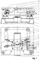
- Arrangements for testing semiconductor wafers as shown in the Drawings are shown, have a base frame 1. With this base frame 1 is a base plate 2 via decoupling members 3 connected. An upper plate 4 is supported Spacer 5 on the base plate 2.
- a positioning device is connected to the base frame 1 6, the horizontal x and horizontal y direction is displaceable.
- the positioning device 6 has a stage 7 on which the chuck 8 can be placed.
- the Chuck 8 is used to hold a semiconductor wafer 9.
- a receiving area 10 is provided in the top of the chuck. Because this receiving area 10 near the top plate 4, that is, over the base plate 2, encompasses the Chuck 8 the base plate 2 spacious, so that a transfer the movement of the positioning device 6 on the chuck 8 is possible.
- tabs 11 are provided, which are located on both sides of the chuck's receiving area. Perpendicular to the tabs 11 are spacers 12 at the outer ends attached, the distance between the stage 7 and the recording plane 13 set the semiconductor wafer 9.
- the chuck 8 is plate-shaped on its top, this surface being at least parallel to the receiving plane 13 of the semiconductor wafer 9 lies.
- the chuck 8 is provided with an opening 14.
- the area of this opening is the area of the semiconductor wafer 9 approximately congruent, so that the semiconductor wafer 9 in the opening 14 can be inserted.
- an annular Provide recording 15 In this annular receptacle 15 an annular groove 16 is introduced through the semiconductor wafer 9 is closable. In this annular groove 16 opens Vacuum channel 17 through a tab 11 and further through Spacer 12 is guided and at the end of the spacer 12th exits so that he is there with a vacuum opening in the stage 7 is connectable.
- a vacuum is a mechanical fastener intended. This consists of a slider 18, which in radial direction to the opening 14 and parallel to the receiving plane 13 is movable and which on the edge of the semiconductor wafer 9 spring-loaded attacks. So that the semiconductor wafer 9 pressed against two pins 19 and thus mechanically fixed.
- This has the advantage that the semiconductor wafer 9 inserted into the opening 14 outside the arrangement can be and is already mechanically fixed. With Placing the chuck 8 on the stage 7 is then the annular groove 16 applied with vacuum, causing the semiconductor wafer 9 is sucked in and held.
- the semiconductor wafer is on the one hand fixed in position and, on the other hand, contacting forces be recorded if the semiconductor wafer on the side 9 is contacted, on which it is also held.
- the base plate 2 is used for receiving of needle holders 20 which carry the contacting needle 21.
- needle holders 20 which carry the contacting needle 21.
- the contacting needles through the opening 14 to the contact pads on the semiconductor wafer Attack 9 and testing can begin.
- an observation microscope 22 arranged between the base plate 2 and the top plate 4.
- the top plate 4 faces in the area above the receiving area 10 of the chuck an observation opening 23. So that will it is possible from above in a manner not shown through this observation opening 23 and through the opening 14 through the overlying rear side of the semiconductor wafer 9 watch while on the front of the wafer 9 attack the contacting needles 21.
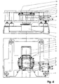
- the contacting needles 21 are on a tester card attached.
- the tester card is on the via an adapter 24 Base plate 2 set.
- those not shown apply Contact pins of the tester card on the one below Front of the semiconductor wafer 9, the back the semiconductor wafer 9 can be observed from above.
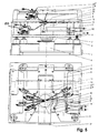
- 5 is a combined possibility of a simultaneous Front and rear side contacting by means of contact needles held in needle holders 20 and 20 ' 21 and 21 '.
- 6 is a simultaneous front and Rear contacting using contacting pins and a simultaneous use of a tester card shown.
- a microscope bridge 25 over the top plate 4 shown on which the not shown Observation microscope can be attached.
Landscapes
- Engineering & Computer Science (AREA)
- Computer Hardware Design (AREA)
- Microelectronics & Electronic Packaging (AREA)
- General Engineering & Computer Science (AREA)
- Physics & Mathematics (AREA)
- General Physics & Mathematics (AREA)
- Testing Or Measuring Of Semiconductors Or The Like (AREA)
- Testing Of Individual Semiconductor Devices (AREA)
- Container, Conveyance, Adherence, Positioning, Of Wafer (AREA)
Description
- Fig. 1
- eine erfindungsgemäße Anordnung in Vorderansicht und Draufsicht für ein Testen einer Halbleiterscheibe mittels von unten angreifenden Kontaktiernadeln,
- Fig. 2
- eine Draufsicht und einen Längsschnitt eines Chuck einer erfindungsgemäßen Testervorrichtung,
- Fig. 3
- ist entfallen,
- Fig. 4
- eine Vorderansicht und Draufsicht einer erfindungsgemäßen Anordnung zum Testen einer Halbleisterscheibe mittels einer von unten angreifenden Testerkarte,
- Fig. 5
- eine Vorderansicht und Draufsicht einer erfindungsgemäßen Anordnung zum Testen einer Halbleiterscheibe mittels von unten und von oben angreifenden Kontaktiernadeln und
- Fig. 6
- eine Vorderansicht und Draufsicht einer erfindungsgemäßen Anordnung zum Testen einer Halbleiterscheibe mittels von unten und oben angreifenden Kontaktiernadeln und einer von unten angreifenden Testerkarte.
- 1
- Grundrahmen
- 2
- Grundplatte
- 3
- Entkopplungsglied
- 4
- Oberplatte
- 5
- Abstandshalter
- 6
- Positioniervorrichtung
- 7
- Bühne
- 8
- Chuck
- 9
- Halbleiterscheibe
- 10
- Aufnanmebereich
- 11
- Lasche
- 12
- Distanzstück
- 13
- Aufnahmeebene
- 14
- Durchbruch
- 15
- ringförmige Aufnahme
- 16
- Ringnut
- 17
- Vakuumkanal
- 18
- Gleitstück
- 19
- Stift
- 20,20'
- Nadelhalter
- 21,21'
- Kontaktiernadel
- 22
- Beobachtungsmikroskop
- 23
- Beobachtungsöffnung
- 24
- Adapter
- 25
- Mikroskopbrücke
Claims (11)
- Anordnung zum Testen von Halbleiterstrukturen, die mit einem Chuck (8) zur Aufnahme einer Halbleiterscheibe (9), welche eine im wesentlichen unstrukturierte Rückseite und eine Vorderseite mit der Struktur der zu testenden Chips aufweist, versehen ist und die zur Halterung von Kontaktiernadeln (21), die auf Kontaktinseln des zu testenden Chips auflegbar sind, mit mehreren Nadelhaltern (20) versehen ist, wobei der Chuck (8) mit Befestigungsmitteln für die Halbleiterscheibe (9) versehen ist und zur Positionierung, mittels einer Positioniervorrichtung gesteuert, relativ zu den Kontaktiernadeln (21) bewegbar ist , dadurch gekennzeichnet, daß der Chuck (8) einen die Rückseite der Halbleiterscheibe (9) nach oben freigebenden Aufnahmebereich (10) mit einer Aufnahmeebene (13) für die Halbleiterscheibe (9) aufweist, wobei die Aufnahmeebene (13) oberhalb des Nadelträgers (20) angeordnet ist, und die Kontaktiernadeln (21) derart nach oben gerichtet sind, daß sie die Kontaktinseln der Halbleiterchips auf der nach unten gerichteten Vorderseite der Halbleiterscheibe (9) kontaktieren.
- Anordnung zum Testen von Halbleiterstrukturen nach Anspruch 1, dadurch gekennzeichnet, daß die Nadelhalter (20) auf einer bezüglich der Bewegung der als x-y-Kreuztisch (6) ausgebildeten Positioniervorrichtung ortsfesten Grundplatte (2) befestigt sind.
- Anordnung zum Testen von Halbleiterstrukturen nach Anspruch 1 oder 2, dadurch gekennzeichnet, daß das Befestigungsmittel als mechanische Halterung und/oder als Vakuumhalterung ausgeführt ist.
- Anordnung zum Testen von Halbleiterstrukturen nach Anspruch 3, dadurch gekennzeichnet, daß die mechanischen Befestigungsmittel aus einem Gleitstück (18) bestehen, das an den Rand der Halbleiterscheibe (9) derart federbelastet angreift, daß die Federkraft den Rand der Halbleiterscheibe (9) gegen gegenüberliegende Anschläge (19) drückt.
- Anordnung zum Testen von Halbleiterstrukturen nach Anspruch 3, dadurch gekennzeichnet, daß als Vakuumhalterung eine Ansaugfläche (15) vorgesehen ist, auf die die Vorderseite oder die Rückseite der Halbleiterscheibe (9) auflegbar ist und die mit einer mit einer Vakuumquelle verbundenen Ansaugnut (16) versehen ist.
- Anordnung zum Testen von Halbleiterstrukturen nach einem der Ansprüche 2 bis 5, dadurch gekennzeichnet, daß der Chuck (8) mit einem mit dem x-y-Kreuztisch (6) verbindbaren und einen Abstand zwischen dem Chuck (8) und dem Kreuztisch (6) realisierenden Distanzstück (12) versehen ist.
- Anordnung zum Testen von Halbleiterstrukturen nach einem der Ansprüche 1 bis 6, dadurch gekennzeichnet, daß die Positioniereinrichtung (6) unter dem Chuck (8) angeordnet ist.
- Anordnung zum Testen von Halbleiterstrukturen nach einem der Ansprüche 1 bis 7, dadurch gekennzeichnet, daß der Chuck (8) derart plattenförmig ausgeführt ist, daß er den Aufnahmebereich (10) für eine Halbleiterscheibe (9) und beidseitig des Aufnahmebereiches (10) angeordnete äußere Laschen (11) aufweist, an deren äußeren Enden die Distanzstücken (12) im wesentlichen senkrecht zu den Laschen (11) befestigt sind.
- Anordnung zum Testen von Halbleiterstrukturen nach einem der Ansprüche 1 bis 8, dadurch gekennzeichnet, daß der Aufnahmebereich (10) einen Durchbruch (14) mit einer zu der Fläche der Halbleiterscheibe (9) zumindest näherungsweise kongruenten Durchbruchsfläche aufweist, wobei auf der den Kontaktnadeln (21) zugewandten Seite des Chuck (8) an dem Durchbruch eine die Durchbruchsfläche verringernde ringförmige Aufnahme (15) vorgesehen ist, daß diese Aufnahme (15) auf der den Kontaktiernadeln (21) abgewandten Seite als Ansaugfläche ausgeführt und mit einer Ringnut (16) versehen ist, in die ein Vakuumkanal (17) mündet.
- Anordnung zum Testen von Halbleiterstrukturen nach Anspruch 8 und 9, dadurch gekennzeichnet, daß der Vakuumkanal (17) durch die äußeren Laschen (11) und das Distanzstück (12) geführt ist, daß eine Aufnahme für ein Distanzstück (12) vorgesehen ist, in die das Distanzstück (12) einsetzbar ist und in der ein mit dem Vakuumkanal (17) des Distanzstückes (12) verbindbarer Vakuumanschluß angeordnet ist.
- Anordnung zum Testen von Halbleiterstrukturen nach einem der Ansprüche 2 bis 9, dadurch gekennzeichnet, daß die Grundplatte (2) Aufnahmemittel für die direkte Aufnahme der Nadelhalter (20) und Aufnahmemittel für die Aufnahme einer zusätzlichen Oberplatte (4) aufweist, die mit Distanzstükken (5) an der Grundplatte (2) befestigbar ist und auf der zusätzliche Nadelhalter (20') befestigbar sind, wobei deren Kontaktnadeln (21') nach unten gerichtet einsetzbar sind.
Applications Claiming Priority (3)
| Application Number | Priority Date | Filing Date | Title |
|---|---|---|---|
| DE19604833A DE19604833C2 (de) | 1996-02-12 | 1996-02-12 | Anordnung zum Testen von Halbleiterstrukturen |
| DE19604833 | 1996-02-12 | ||
| PCT/DE1997/000260 WO1997029380A1 (de) | 1996-02-12 | 1997-02-12 | Anordnung zum testen von halbleiterstrukturen |
Publications (2)
| Publication Number | Publication Date |
|---|---|
| EP0880706A1 EP0880706A1 (de) | 1998-12-02 |
| EP0880706B1 true EP0880706B1 (de) | 2002-09-25 |
Family
ID=7785006
Family Applications (1)
| Application Number | Title | Priority Date | Filing Date |
|---|---|---|---|
| EP97917220A Expired - Lifetime EP0880706B1 (de) | 1996-02-12 | 1997-02-12 | Anordnung zum testen von halbleiterstrukturen |
Country Status (4)
| Country | Link |
|---|---|
| US (1) | US6373272B1 (de) |
| EP (1) | EP0880706B1 (de) |
| DE (1) | DE19604833C2 (de) |
| WO (1) | WO1997029380A1 (de) |
Families Citing this family (4)
| Publication number | Priority date | Publication date | Assignee | Title |
|---|---|---|---|---|
| US7315299B2 (en) * | 2002-08-01 | 2008-01-01 | Nissan Motor Co., Ltd. | Multi-way input device and operating failure avoidance method using the same |
| DE102006038457B4 (de) * | 2006-08-16 | 2014-05-22 | Cascade Microtech, Inc. | Verfahren und Vorrichtung zum Temperieren elektronischer Bauelemente |
| US7425839B2 (en) * | 2006-08-25 | 2008-09-16 | Micron Technology, Inc. | Systems and methods for testing packaged microelectronic devices |
| CN120854372B (zh) * | 2025-09-23 | 2025-11-21 | 达波科技(上海)有限公司 | 一种手持式晶圆真空吸笔 |
Family Cites Families (14)
| Publication number | Priority date | Publication date | Assignee | Title |
|---|---|---|---|---|
| US3661316A (en) * | 1970-04-13 | 1972-05-09 | Kulicke & Soffa Ind Inc | Aiming device for semiconductor bonding apparatus |
| US3702439A (en) * | 1970-08-12 | 1972-11-07 | Bell Telephone Labor Inc | Low impedance fixed point test probe |
| US3866119A (en) * | 1973-09-10 | 1975-02-11 | Probe Rite Inc | Probe head-probing machine coupling adaptor |
| US3936743A (en) * | 1974-03-05 | 1976-02-03 | Electroglas, Inc. | High speed precision chuck assembly |
| US3996517A (en) | 1975-12-29 | 1976-12-07 | Monsanto Company | Apparatus for wafer probing having surface level sensing |
| FR2645679B1 (fr) * | 1989-04-07 | 1994-05-06 | Onera (Off Nat Aerospatiale) | Installation de test, en particulier pour plaquettes de materiau semi-conducteur |
| JPH04104216A (ja) * | 1990-08-24 | 1992-04-06 | Hitachi Koki Co Ltd | 光走査装置 |
| US5404111A (en) * | 1991-08-03 | 1995-04-04 | Tokyo Electron Limited | Probe apparatus with a swinging holder for an object of examination |
| JPH0714898A (ja) * | 1993-06-23 | 1995-01-17 | Mitsubishi Electric Corp | 半導体ウエハの試験解析装置および解析方法 |
| US6025732A (en) * | 1993-07-09 | 2000-02-15 | Aehr Test Systems | Reusable die carrier for burn-in and burn-in process |
| JP3300479B2 (ja) * | 1993-07-19 | 2002-07-08 | 浜松ホトニクス株式会社 | 半導体デバイス検査システム |
| US6002792A (en) * | 1993-11-16 | 1999-12-14 | Hamamatsu Photonics Kk | Semiconductor device inspection system |
| DE69529501T2 (de) * | 1994-04-18 | 2003-12-11 | Micron Technology, Inc. | Verfahren und vorrichtung zum automatischen positionieren elektronischer würfel in bauteilverpackungen |
| JPH08213128A (ja) * | 1995-02-08 | 1996-08-20 | Texas Instr Japan Ltd | ソケット |
-
1996
- 1996-02-12 DE DE19604833A patent/DE19604833C2/de not_active Expired - Fee Related
-
1997
- 1997-02-12 US US09/142,391 patent/US6373272B1/en not_active Expired - Fee Related
- 1997-02-12 WO PCT/DE1997/000260 patent/WO1997029380A1/de not_active Ceased
- 1997-02-12 EP EP97917220A patent/EP0880706B1/de not_active Expired - Lifetime
Also Published As
| Publication number | Publication date |
|---|---|
| WO1997029380A1 (de) | 1997-08-14 |
| EP0880706A1 (de) | 1998-12-02 |
| DE19604833A1 (de) | 1997-08-14 |
| US6373272B1 (en) | 2002-04-16 |
| DE19604833C2 (de) | 2000-08-10 |
Similar Documents
| Publication | Publication Date | Title |
|---|---|---|
| DE10297763B4 (de) | Prüfgerät für elektronische Bauelemente | |
| DE69710185T2 (de) | Vibrationsstabilisator für emissionsmikroskop | |
| DE10297654B4 (de) | Halteeinsatz und Handhabungsvorrichtung mit einem solchen Halteeinsatz für elektronische Bauelemente | |
| DE69026603T2 (de) | Plattenhalter in einer bohrmaschine für gedruckte schaltungen | |
| DE112008002615B4 (de) | Verfahren zur Prüfung eines Testsubstrats unter definierten thermischen Bedingungen und thermisch konditionierbarer Prober | |
| DE10004193C2 (de) | Trägerhandhabungsvorrichtung für ein IC-Modulhandhabungsgerät sowie Verfahren dafür | |
| DE102010049326A1 (de) | Elektrische Verbindungsvorrichtung und Testsystem zur Verwendung derselben | |
| DE19914775A1 (de) | IC-Prüfgerät | |
| DE60222021T2 (de) | Prüfkartenabdecksystem und -verfahren | |
| DE10246282B4 (de) | Prober zum Testen von Substraten bei tiefen Temperaturen | |
| DE102007054879A1 (de) | Verfahren und Anordnung zur Positionierung einer Probecard | |
| DE10228290B4 (de) | Halbleitervorrichtungssockel | |
| EP0411003A1 (de) | Greifvorrichtung. | |
| DE102004030881B4 (de) | Verfahren und Prober zur Kontaktierung einer Kontakfläche mit einer Kontaktspitze | |
| DE19604833C2 (de) | Anordnung zum Testen von Halbleiterstrukturen | |
| US6811072B2 (en) | Known good die removal method and apparatus | |
| DE10061628B4 (de) | Vorrichtung und Verfahren zum Ergreifen und Transportieren von Wafern | |
| DE3931305A1 (de) | Pruefkartenvorrichtung | |
| EP1739440A2 (de) | Elektrisches Prüfverfahren und -vorrichtung sowie Verfahren zur Herstellung einer Kontaktiervorrichtung | |
| DE10028569A1 (de) | Vorrichtung zum Positionieren scheibenförmiger Objekte | |
| EP1422986A1 (de) | Chipübergabestation einer Bondmaschine | |
| DE212019000102U1 (de) | Nukleinsäureamplifikations-Detektionsvorrichtung und Diagnoseanalysator | |
| DE102022206758A1 (de) | Prüfvorrichtung und prüfverfahren | |
| EP1793232A2 (de) | Elektrische Kontakteinrichtung und Prüfvorrichtung für die Prüfung eines elektrischen Prüflings | |
| DE102004041102A1 (de) | Anordnung und Verfahren zum Testen von Substraten unter Belastung |
Legal Events
| Date | Code | Title | Description |
|---|---|---|---|
| PUAI | Public reference made under article 153(3) epc to a published international application that has entered the european phase |
Free format text: ORIGINAL CODE: 0009012 |
|
| 17P | Request for examination filed |
Effective date: 19980808 |
|
| AK | Designated contracting states |
Kind code of ref document: A1 Designated state(s): BE CH FR GB IT LI |
|
| 17Q | First examination report despatched |
Effective date: 19991115 |
|
| GRAG | Despatch of communication of intention to grant |
Free format text: ORIGINAL CODE: EPIDOS AGRA |
|
| GRAG | Despatch of communication of intention to grant |
Free format text: ORIGINAL CODE: EPIDOS AGRA |
|
| GRAH | Despatch of communication of intention to grant a patent |
Free format text: ORIGINAL CODE: EPIDOS IGRA |
|
| GRAH | Despatch of communication of intention to grant a patent |
Free format text: ORIGINAL CODE: EPIDOS IGRA |
|
| GRAA | (expected) grant |
Free format text: ORIGINAL CODE: 0009210 |
|
| RIN1 | Information on inventor provided before grant (corrected) |
Inventor name: RUNGE, DIETMAR Inventor name: HUELSMANN, THOMAS Inventor name: DIETRICH, CLAUS Inventor name: WELSCH, REINHARD |
|
| AK | Designated contracting states |
Kind code of ref document: B1 Designated state(s): BE CH FR GB IT LI |
|
| PG25 | Lapsed in a contracting state [announced via postgrant information from national office to epo] |
Ref country code: IT Free format text: LAPSE BECAUSE OF FAILURE TO SUBMIT A TRANSLATION OF THE DESCRIPTION OR TO PAY THE FEE WITHIN THE PRESCRIBED TIME-LIMIT;WARNING: LAPSES OF ITALIAN PATENTS WITH EFFECTIVE DATE BEFORE 2007 MAY HAVE OCCURRED AT ANY TIME BEFORE 2007. THE CORRECT EFFECTIVE DATE MAY BE DIFFERENT FROM THE ONE RECORDED. Effective date: 20020925 |
|
| REG | Reference to a national code |
Ref country code: GB Ref legal event code: FG4D Free format text: NOT ENGLISH |
|
| REG | Reference to a national code |
Ref country code: CH Ref legal event code: EP |
|
| GBT | Gb: translation of ep patent filed (gb section 77(6)(a)/1977) |
Effective date: 20030128 |
|
| PG25 | Lapsed in a contracting state [announced via postgrant information from national office to epo] |
Ref country code: LI Free format text: LAPSE BECAUSE OF NON-PAYMENT OF DUE FEES Effective date: 20030228 Ref country code: CH Free format text: LAPSE BECAUSE OF NON-PAYMENT OF DUE FEES Effective date: 20030228 Ref country code: BE Free format text: LAPSE BECAUSE OF NON-PAYMENT OF DUE FEES Effective date: 20030228 |
|
| RAP2 | Party data changed (patent owner data changed or rights of a patent transferred) |
Owner name: SUSS MICROTEC TESTSYSTEME GMBH |
|
| ET | Fr: translation filed | ||
| PLBE | No opposition filed within time limit |
Free format text: ORIGINAL CODE: 0009261 |
|
| STAA | Information on the status of an ep patent application or granted ep patent |
Free format text: STATUS: NO OPPOSITION FILED WITHIN TIME LIMIT |
|
| REG | Reference to a national code |
Ref country code: FR Ref legal event code: TP |
|
| 26N | No opposition filed |
Effective date: 20030626 |
|
| REG | Reference to a national code |
Ref country code: CH Ref legal event code: PL |
|
| PGFP | Annual fee paid to national office [announced via postgrant information from national office to epo] |
Ref country code: GB Payment date: 20040119 Year of fee payment: 8 |
|
| PG25 | Lapsed in a contracting state [announced via postgrant information from national office to epo] |
Ref country code: GB Free format text: LAPSE BECAUSE OF NON-PAYMENT OF DUE FEES Effective date: 20050212 |
|
| GBPC | Gb: european patent ceased through non-payment of renewal fee |
Effective date: 20050212 |
|
| PGFP | Annual fee paid to national office [announced via postgrant information from national office to epo] |
Ref country code: FR Payment date: 20110314 Year of fee payment: 15 |
|
| REG | Reference to a national code |
Ref country code: FR Ref legal event code: ST Effective date: 20121031 |
|
| PG25 | Lapsed in a contracting state [announced via postgrant information from national office to epo] |
Ref country code: FR Free format text: LAPSE BECAUSE OF NON-PAYMENT OF DUE FEES Effective date: 20120229 |