EP0879304B1 - Herstellung von schrägen galvanikstrukturen - Google Patents
Herstellung von schrägen galvanikstrukturen Download PDFInfo
- Publication number
- EP0879304B1 EP0879304B1 EP97916314A EP97916314A EP0879304B1 EP 0879304 B1 EP0879304 B1 EP 0879304B1 EP 97916314 A EP97916314 A EP 97916314A EP 97916314 A EP97916314 A EP 97916314A EP 0879304 B1 EP0879304 B1 EP 0879304B1
- Authority
- EP
- European Patent Office
- Prior art keywords
- process according
- substrate
- structured
- mentioned
- conductive
- Prior art date
- Legal status (The legal status is an assumption and is not a legal conclusion. Google has not performed a legal analysis and makes no representation as to the accuracy of the status listed.)
- Expired - Lifetime
Links
Images



Classifications
-
- H—ELECTRICITY
- H10—SEMICONDUCTOR DEVICES; ELECTRIC SOLID-STATE DEVICES NOT OTHERWISE PROVIDED FOR
- H10P—GENERIC PROCESSES OR APPARATUS FOR THE MANUFACTURE OR TREATMENT OF DEVICES COVERED BY CLASS H10
- H10P14/00—Formation of materials, e.g. in the shape of layers or pillars
- H10P14/40—Formation of materials, e.g. in the shape of layers or pillars of conductive or resistive materials
- H10P14/46—Formation of materials, e.g. in the shape of layers or pillars of conductive or resistive materials using a liquid
- H10P14/47—Electrolytic deposition, i.e. electroplating; Electroless plating
-
- C—CHEMISTRY; METALLURGY
- C25—ELECTROLYTIC OR ELECTROPHORETIC PROCESSES; APPARATUS THEREFOR
- C25D—PROCESSES FOR THE ELECTROLYTIC OR ELECTROPHORETIC PRODUCTION OF COATINGS; ELECTROFORMING; APPARATUS THEREFOR
- C25D1/00—Electroforming
- C25D1/003—3D structures, e.g. superposed patterned layers
-
- C—CHEMISTRY; METALLURGY
- C25—ELECTROLYTIC OR ELECTROPHORETIC PROCESSES; APPARATUS THEREFOR
- C25D—PROCESSES FOR THE ELECTROLYTIC OR ELECTROPHORETIC PRODUCTION OF COATINGS; ELECTROFORMING; APPARATUS THEREFOR
- C25D1/00—Electroforming
- C25D1/10—Moulds; Masks; Masterforms
-
- G—PHYSICS
- G02—OPTICS
- G02B—OPTICAL ELEMENTS, SYSTEMS OR APPARATUS
- G02B26/00—Optical devices or arrangements for the control of light using movable or deformable optical elements
- G02B26/08—Optical devices or arrangements for the control of light using movable or deformable optical elements for controlling the direction of light
- G02B26/0816—Optical devices or arrangements for the control of light using movable or deformable optical elements for controlling the direction of light by means of one or more reflecting elements
- G02B26/0833—Optical devices or arrangements for the control of light using movable or deformable optical elements for controlling the direction of light by means of one or more reflecting elements the reflecting element being a micromechanical device, e.g. a MEMS mirror, DMD
-
- G—PHYSICS
- G02—OPTICS
- G02B—OPTICAL ELEMENTS, SYSTEMS OR APPARATUS
- G02B26/00—Optical devices or arrangements for the control of light using movable or deformable optical elements
- G02B26/08—Optical devices or arrangements for the control of light using movable or deformable optical elements for controlling the direction of light
- G02B26/0816—Optical devices or arrangements for the control of light using movable or deformable optical elements for controlling the direction of light by means of one or more reflecting elements
- G02B26/0833—Optical devices or arrangements for the control of light using movable or deformable optical elements for controlling the direction of light by means of one or more reflecting elements the reflecting element being a micromechanical device, e.g. a MEMS mirror, DMD
- G02B26/0841—Optical devices or arrangements for the control of light using movable or deformable optical elements for controlling the direction of light by means of one or more reflecting elements the reflecting element being a micromechanical device, e.g. a MEMS mirror, DMD the reflecting element being moved or deformed by electrostatic means
-
- G—PHYSICS
- G03—PHOTOGRAPHY; CINEMATOGRAPHY; ANALOGOUS TECHNIQUES USING WAVES OTHER THAN OPTICAL WAVES; ELECTROGRAPHY; HOLOGRAPHY
- G03F—PHOTOMECHANICAL PRODUCTION OF TEXTURED OR PATTERNED SURFACES, e.g. FOR PRINTING, FOR PROCESSING OF SEMICONDUCTOR DEVICES; MATERIALS THEREFOR; ORIGINALS THEREFOR; APPARATUS SPECIALLY ADAPTED THEREFOR
- G03F7/00—Photomechanical, e.g. photolithographic, production of textured or patterned surfaces, e.g. printing surfaces; Materials therefor, e.g. comprising photoresists; Apparatus specially adapted therefor
-
- H—ELECTRICITY
- H05—ELECTRIC TECHNIQUES NOT OTHERWISE PROVIDED FOR
- H05K—PRINTED CIRCUITS; CASINGS OR CONSTRUCTIONAL DETAILS OF ELECTRIC APPARATUS; MANUFACTURE OF ASSEMBLAGES OF ELECTRICAL COMPONENTS
- H05K3/00—Apparatus or processes for manufacturing printed circuits
- H05K3/22—Secondary treatment of printed circuits
- H05K3/24—Reinforcing of the conductive pattern
- H05K3/241—Reinforcing of the conductive pattern characterised by the electroplating method; means therefor, e.g. baths or apparatus
Definitions
- the technical field of the invention is the production of three-dimensional customizable electroplating structures on substrates that are still in the prior art Structuring by photoresist and subsequent galvanic deposition Get opportunities and barriers.
- the prior art explains the formation of electroplating structures that are electrical are conductive and find a wide range of applications in micromechanics Apply a light-sensitive varnish by exposing and removing certain Parts of the applied paint and subsequent galvanic deposition a galvanic fluid that is connected to a first potential, while the electrically conductive base on the substrate as a plating base electrically with the opposite potential is applied.
- the electroplating structures produced in this way have regular vertical edge areas because the light on the Photoresist always strikes vertically, so that only vertical varnish structures arise can. Accordingly, only those electroplating structures can arise whose Edge areas run in the direction in which the light has also entered.
- the invention has set itself the task of giving up the lacquer structures given by the incident light as a template for electroplating structures and making it possible to create freely designable electroplating structures whose edge surfaces no longer necessarily have to run vertically or almost vertically. To this end, the invention proposes solutions according to claim 1, claim 16 and claim 23.
- those that can be designed in the vertical direction are galvanized deposited structures formed as profiles on the substrate if the previously applied conductive layer is structured in plane directions (lateral direction) (Claim 1).
- the three-dimensional metal structure that can be formed during electroplating becomes also formed if the substrate carries at least one conductive layer, one of the several or one is structured by a conductive layer in the lateral direction Formation of several island areas that have no or no significant areas have electrical wiring, and when galvanizing one of the island areas as Core area is switched cathodically (claim 16).
- the manufacturing result - circumscribed based on the method steps - is covered in claim 23, it results either based on the method according to claim 16 or based on the method according to claim 1.
- the three-dimensionally shaped massive Metal structure with a clear extension in the vertical direction can be recognized that not all vertical edge surfaces of this structure are mandatory must run in a vertical or almost vertical direction. That describes however not that all edges are now mandatory in oblique or curved path run, but only that at least one of the vertical flanks an oblique or is a curved plane that could not be designed with previous manufacturing processes.
- a surface in the form of a laterally deposited layer is the one according to the invention "Profile" is not.
- photoresist is still used, it no longer forms the core and the basis for a galvanic impression based on exposed and etched Lead structures based on a photoresist layer.
- This varnish is used according to the Invention for the design of a three-dimensional structure in the vertical direction, if it covers most of the core area and only a small section released, can pass through the cathodic potential in the electroplating bath. Starting from the potential in the electroplating fluid, one slowly forms growing layer on the small area with cathodic potential. This Layer grows in the vertical direction and inevitably widens in the process slightly in the lateral direction.
- the new procedure allows the lateral growth rate to be briefly described control, on the one hand by length and duration of the electroplating, on the other - before the start of the Electroplating - by applying certain geometric designs as a structure in the Plating base exposed to the electroplating bath during electroplating.
- the ratio of lateral to vertical growth rate gives the electroplating profile.
- the electroplating structures can consist of gold or nickel.
- the electrically conductive Starting layer (plating base) can be formed from the same materials. Become several plating bases are used, so they are isolated from intermediate layers, preferably SiN layers. If only one plating base is used, this can The substrate itself must be insulating and an additional insulating layer must be applied to the substrate not be applied.
- the manufacturing method according to the invention works without thick layers of lacquer, it forms there is no side frame for those vertical surfaces that are not shaped obliquely should be. It is then possible to use the sloping electroplating structure in all directions, e.g. circular or elliptical, to grow up. When using concentric island areas to control the lateral growth rate can also create concave or convex shapes with an almost unlimited height h.
- thick lacquer structures can also advantageously be combined with the completely free plating base structure, so that in certain areas Growth rate in the lateral direction (x and y direction) is limited and limited in the other direction is predefined due to the structured plating base.
- the method according to the invention is very cost-effective; it is particularly cost-effective compared to a known gray-tone lithography process , since this technology is based on making the structures in the mask design smaller than the resolution of the lithography.
- the gray-tone lithography no longer creates light / dark areas, but a mixture of gray tones, which is only achieved with a very complex mask design and requires stepper exposure with a reduction optics (cf. "Microfabrication of complex surface topographies" in Sensors and Actuators, A 46-47, pages 89-94, 1995).
- the invention allows the formation of solid galvanic structures without underlying lacquer layers and without using stepper exposure only through use simple and widely used UV contact imagesetter. These devices are much cheaper and the results they achieve are accordingly cheaper.
- X-ray lithographs for structuring the thick lacquers used, so three-dimensional structures of several 100 microns Height can be achieved.
- LIGA technology X-ray lithographs
- the height of the thick (structured) lacquer layer is limited to approx. 100 ⁇ m, due to the maximum exposure depth of this process.
- the barrier thus formed only applies for the manufacturing processes that are based on thick photoresists, those Manufacturing method of the invention without the paint boundaries as the edge areas of the Electroplating are not limited in their height by this exposure depth, the height is formed solely on the basis of the time during which the electroplating impression is taken is carried out.
- an inclined structure on a substrate 10 is used in micromechanics (cf. FIG . 12 ).
- a desired pivoting movement ⁇ of a tilting mirror 40 which rests on a pin, is significantly increased at lower electrostatic potentials (+) and (-) if structures that are close to the tilting movement are used, such as the wedge-shaped inclined structures 20a with the height h on the left and to the right of the tilt mirror stator journal.
- FIG. 13 shows that a pivoting movement ⁇ of a tilting mirror 30 there is only slight, when using the same potentials, if flat electroplating structures 90, 91 with a much smaller height h 1 are used.
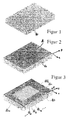
- the plating base 11 itself is structured in the x, y plane to form conductive island regions 12 i , which in this example are lines 12 8 , 12 9 , 12 10 are formed in a window left free from the core region 11a of the plating base 11.
- Circumferentially around the line structure of the structured island region 12 i runs an insulating strip 13a, the k i insulating separating the core region 11 of the island portion 12th
- the strip 13a is the surface of the insulating substrate 10. If the substrate 10 itself is not insulating, 13a would be a section of an intermediate insulating layer between the plating base 11 from FIG. 2 and a conductive substrate 10.
- Insulating is to be understood in such a way that it must not be an essential power line; a lower leakage current that does not significantly lead to the formation of a strongly negative potential on the islands 12 i is harmless.
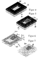
- a thick photoresist layer 14 is applied to the core region 11 k of FIG. 3, this thick lacquer layer 14 is partially exposed again (in the window) and results in the product according to FIG. 4.
- the conductive core 11k of the plating is still on a small partial strip 11k ' Base 11 can be seen, the rest of the core area is covered by the lacquer layer 14.
- the structured plating base region 12 i with the large number of strip-shaped islands thus remains free.
- the electroplating takes place in the area 11k 'and from there the electroplating structure 20a grows in the growth direction -y, if the coordinate system y, x, h (y, x) of FIG. 6 and FIG. 3 is used as a basis.
- the growth in the growth direction -y is controlled by the distance, width and geometry of the isolated metal strips which are fixed before the start of the electroplating bath.
- the electroplating material also grows upwards perpendicular to the plane of the substrate 10 and is delimited by the lacquer in three lateral directions. In the direction not delimited by the lacquer 14, there is permanent growth in the -y and in the h direction by overplating from island to island.
- the electroplating structure initially grows vertically and only slowly over the isolated intermediate area until it reaches the closest island area. This is illustrated with the aid of FIG. 9 , which can be placed next to FIG. 5 in order to illustrate the step galvanizing over the isolated areas between the islands 12 1 , 12 2 , 12 3 etc.
- the lateral growth rate increases abruptly and the vertical growth rate decreases for a moment.
- the lateral growth rate then drops again and the vertical growth rate increases.
- an area is alternately galvanized in the lateral direction in order to then grow again in the vertical direction.
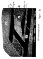
- FIGS. 11a and 11b show electroplating structures which have been produced using the method described, with two-sided delimitation using a lacquer structure.
- a hill-shaped electroplating structure 20 'or 20a is formed with two inclined surfaces and a crest, the zenith lies above the cathode strip 11k, which corresponds to the strip 11k' of FIG. 9 and FIG. 4.
- Metallic strips 12 1 , 12 2 , 12 3 , etc., insulated therefrom are laterally spaced, as can also be seen in FIG. 9.
- the step-by-step electroplating with the vertical electroplating can be seen particularly clearly in the right-hand edge zones of FIG. 11b, where the slope still shows clear traces of the stripe structure forming it.
- the channel structure is only leveled out in areas higher up and an almost flat slope is created.
- the control of the helix angle according to FIG. 10 takes place via the definition of the Distance s according to Figure 10a and the width I of the strips. Will other structures chosen that are not stripes, but concentric or elliptical shapes, see above the function of FIG. 10 can be changed accordingly. Generally oriented the wedge angle of the bevel formed by the fact that a larger distance s and a smaller strip width I both cause the wedge angle to become larger. Are the Distances s are not the same in the x direction, so structures other than inclined structures can be used generated, the angle of the wedge surface is then dependent on the distance to Cathode area 11k '.
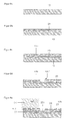
- FIGS . 8a to 8e An alternative manufacturing method is described in FIGS . 8a to 8e .
- a first plating layer 23 is applied as a conductive starting layer (FIG. 8b).
- An insulating layer 13b is placed on this conductive layer 23, for example by vapor deposition or by sputtering.
- a core region 23 k of the otherwise covered first conductive layer 23 is exposed at a suitable point in the insulating layer.
- the corresponding window is designated 13b ', the electrical contact to the electroplating fluid can be formed here.
- the hidden conductive layer 23 serves as a power supply or discharge ( Figure 8d, Figure 8e).
- Island regions 22 i are formed on the insulating layer 13b, which are structured either by introducing the window according to FIG. 8b or thereafter from a second plating layer (by coating and exposure). These island regions 23 i are electrically insulated from the first conductive layer 23 (FIG. 8e).
- FIG. 8e thus forms a basis for growth rates running in all directions of the plane x / y, controlled and influenced by the structure of the island regions 22 i above and isolated from the inner conductive layer 23.
- the electrical potentials (+) and (-) which are applied to the electroplating fluid GF or the conductive layer 23 are indicated schematically in FIG. 8e.
- the island areas 22 i are not connected (nc).
- a structured surface arises from an extensive one conductive layer that has been sputtered or evaporated, the Metal type of the layer depends on the chosen (following) electroplating.
- a lacquer with a thin, e.g. 1 ⁇ m thick structure-lacquer layer follows and in a lithography process the structure of the conductivity layer can be exposed and exposed (etching or ion milling).
- galvanic pre-molding can be used connect to make the structure more stable.
- Metal can also be added are sputtered with a small thickness of about 100 nm.
Landscapes
- Chemical & Material Sciences (AREA)
- Physics & Mathematics (AREA)
- General Physics & Mathematics (AREA)
- Materials Engineering (AREA)
- Electrochemistry (AREA)
- Metallurgy (AREA)
- Organic Chemistry (AREA)
- Chemical Kinetics & Catalysis (AREA)
- Engineering & Computer Science (AREA)
- Optics & Photonics (AREA)
- Crystallography & Structural Chemistry (AREA)
- Electroplating Methods And Accessories (AREA)
- Cultivation Of Seaweed (AREA)
- Manufacturing Of Printed Wiring (AREA)
- Micromachines (AREA)
- Electrochromic Elements, Electrophoresis, Or Variable Reflection Or Absorption Elements (AREA)
Description
- Figur 1
- veranschaulicht das Substrat 10.
- Figur 2
- zeigt den Verfahrensschritt, in dem eine leitende Startschicht (Plating-Base) 11 auf das Substrat 10 aufgebracht worden ist.
- Figur 3
- verdeutlicht die laterale Strukturierung der Plating-Base unter Bildung eines Kernbereiches 11k und eines aus einer Vielzahl von Inseln bestehenden Insel-Bereiches 12i, wobei alle Inseln voneinandern isoliert angeordnet sind. Der entsprechende Isolierring 13a liegt innerhalb des vom Kernbereich 11a belassenen Fensters, in dem ohne elektrischen Kontakt zum Kernbereich 11k die einzelnen isolierten Inselbereiche 12i als linienförmige und voneinander beabstandete Streifen 128,129,1210... angeordnet sind.
- Figur 4
- veranschaulicht als eine Verfahrensvariante das Aufbringen einer dicken Lackschicht 14 auf den Kernbereich 11k unter Freilassung des Inselbereiches 12i mit der strukturierten Plating-Base. Die quaderförmige Lackschicht 14 mit Fenster kann in mehreren Stufen hergestellt sein, durch Belacken und Lithographie.
- Figur 5
- zeigt das Ergebnis der Galvanikabformung durch einen Schrägbereich 20a, der sich innerhalb des Fensters der Figur 4 bildet, wenn der Kernbereich 11k' kathodisch geschaltet wird und die Inselbereiche 12i elektrisch nicht angeschlossen werden (n.c.).
- Figur 6
- zeigt das Verfahrensergebnis nach Entfernen der Lackschicht 14, wobei die als Kernbereich zuvor erläuterte Plating-Base 11k noch verbleibt und der Schrägbereich 20a deutlich von dem Substrat 10 mit der Höhe hmax hervorsteht.
- Figur 7
- zeigt das Verfahrensergebnis nach Entfernen des Kernbreiches 11k der Plating-Base, wobei auch der strukturierte Teil 12i der Plating-Base entfernt werden kann.
- Figur 8a bis Figur 8e
- zeigt ein alternatives Galvanikverfahren zur Herstellung eines Schräggebildes, wie das der Figur 7, indem zwei übereinander aufgebrachte leitfähige Schichten voneinander durch eine Isolierschicht 13b getrennt sind und ein Fenster 13b' einen Teil 23k der ersten Leitschicht 23 freilegt, um gemeinsam mit dem Inselbreich 22i, der aus der zweiten Leitschicht gebildet wurde, eine in Lateralrichtung gesteuerte Aufwachsrate zu erhalten. Schematisch ist in der Figur 8e die elektrische Verbindung (+) und (-) sowie n.c. angedeutet, wobei das positive Potential (+) am Galvanikfluid GF angelegt wird, das negative Potential (-) an der tiefer liegenden Plating-Base 23 und die Inselbereiche 22i elektrisch nicht angeschlossen werden (not connected).
- Figur 9
- veranschaulicht in einem seitlichen Schnitt das lateral gesteuerte Aufwachsen der Galvaniksubstanz G, orientiert an einem Kernbereich 11k und davon beabstandeter Inselbereiche 121,122...12i, die elektrisch über das Substrat 10 oder eine zusätzliche Isolierlage 13a von dem Kernbereich 11k isoliert sind.
- Figur 10 und Figur 10a
- verdeutlichen eine Einstellung für die entstehende Schrägstruktur, wobei der Schrägwinkel auf der Ordinate gegenüber dem Verhältnis von Insellänge I zu Zwischenabstand s aufgetragen ist. Je geringer die Breite jeder Insel (line) in x-Richtung ist und je größer der Abstand zweier Inseln (space) ist, desto steiler wird der Keilwinkel der beim Galvanisieren abgeformten Struktur.
- Figur 11a und Figur 11b
- zeigen eine Nickelgalvanik und eine Goldgalvanik mit Schrägstruktur 20',20a auf einem strukturierten Substrat, das aus voneinander isolierten Streifen besteht, die den zuvor erwähnten Inselbereich bilden. Ein Streifen 11k ist gegenüber den anderen Streifen verlängert und dient als Kernbereich, für kathodisches Potential.
- Figur 12
- zeigt als ein Einsatzgebiet der Schräggalvanik einen Kippspiegel 40, der mit Keilstrukturen in seiner Schwenklage α verändert wird, wobei geringere Spannungen benötigt werden, um einen höheren Stellwinkel zu erzielen, gegenüber der in Figur 13 dargestellten Kippspiegel-Variante 30 mit ebenen Galvanikstrukturen.
- Figur 13
- zeigt einen Kippspiegel 30 mit ebenen Galvanikstrukturen 91,90, der - bei gleicher Steuerspannung - nur einen geringen Stellwinkel β aufweist.
- Figur 14
- verdeutlicht eine in zwei Ebenen-Richtungen x,y aufwachsenden Keilstruktur 20a, deren Randbereiche 20b nicht senkrecht zum Substrat 10 verlaufen, sondern eine deutlich gekrümmte Randfläche bilden, nach Art einer 1-e-Funktion.
Claims (23)
- Herstellverfahren für ein in Höhenrichtung [h(x,y)] gestaltetes galvanisch abgeschiedenes Metallprofil (G;20a,20b;20') auf einem Substrat (10), wobei(a) eine zuvor aufgebrachte leitfähige Schicht (11,21,23) in Lateralrichtung (x,y) in einen ersten (11k,-) und mehrere zweite Bereiche (12i) strukturiert wird;(b) der erste Bereich (11k,-) der strukturierten leitfähigen Schicht (11,23) auf ein kathodisches Potential gebracht wird, um dort mit der galvanischen Abscheidung (G) zu beginnen;(c) ein Übergalvanisieren über isolierte Strecken (10,13) hin zu den individuell leitfähigen aber elektrisch nicht angeschlossenen zweiten Bereichen der Lateralstruktur erfolgt, um das leitende Metallprofil (G;20a,20b;20') zu bilden.
- Verfahren nach Anspruch 1, bei dem die Strukturierung aus der Gestaltung eines Kernbereiches (11k,23k; k=1...n) und davon beabstandeten Inselbereichen (12i; 22i; i=1...m) besteht, welch letztere vom Kernbereich und weitgehend untereinander isoliert sind.
- Verfahren nach einem der erwähnten Ansprüche, wobei beim Galvanisieren (Beschichten mit elektrisch leitfähigen Substanzen) die Kern- bzw. Inselbereiche (11k,23k,12i,22i) unterschiedliche Potentiale haben, insbesondere kathodisches Potential bzw. demgegenüber im wesentlichen isoliert sind.
- Verfahren nach einem der erwähnten Ansprüche, bei dem die laterale Strukturierung erfolgt, indem die aufgebrachte leitfähige Schicht (11,23) dünn mit lichtempfindlichem Lack beschichtet wird und in einem Lithographieverfahren lateral (x,y) strukturiert wird.
- Verfahren nach Anspruch 4, bei dem die mit dünnem Lack strukturierte Flächeum voneinander beabstandete Leitbereiche (11k,12i;23k,22i) zu schaffen.(a) galvanisch abgeformt wird; oder(b) durch Aufbringen (Sputtern, Dampfen) von Metall strukturiert beschichtet wird;
- Verfahren nach einem der erwähnten Ansprüche, bei dem auf der (strukturierten) leitfähigen Schicht (11) eine dicke Schicht aus Lack (14) aufgebracht wird, in den Inselbereichen (12i) freibelichtet und freigelegt sowie von dem Kernbereich (11k,23k) zumindest ein Teilbereich (11k',23k) freigelegt werden.
- Verfahren nach einem der erwähnten Ansprüche, bei dem der Kernbereich (23k) tiefer liegt als die Inselbereiche (22i) und die beiden Bereiche von einer Isolationsschicht (13) getrennt sind.
- Verfahren nach einem der erwähnten Ansprüche, bei dem der nicht lateral strukturierte Teil (11k,23k) der aufgebrachten Schicht (Plating-Base; 11,23) nach Ausformen der in Höhenrichtung gestaltbaren (h(x,y)) galvanisch abgeschiedenen Struktur vom Substrat (10) entfernt wird, zuvor ggf. der darauf aufgebrachte (dicke) Lackbereich (14) entfernt wird.
- Verfahren nach einem der erwähnten Ansprüche, bei dem die Höhe der galvanisch abgeformten Struktur im Größenbereich von 1µm bis 100µm liegt, insbesondere unterhalb 10µm.
- Verfahren nach einem der erwähnten Ansprüche, bei dem das Metallprofil eine Schrägstruktur ist.
- Verfahren nach einem der erwähnten Ansprüche, bei dem zwischen Substrat (10) und erster Plating-Base (11) eine Isolierschicht (13a), insbesondere aus SiN, aufgebracht wird.
- Verfahren nach einem der erwähnten Ansprüche, bei dem durch Variation des Abstandes (s), der Breite (I) und/oder der Geometrie der Inselbereiche gegenüber dem Kernbereich die Form der durch Galvanikabscheidung gebildeten Struktur veränderbar ist bzw. verändert wird (Fig. 10).
- Verfahren nach einem der erwähnten Ansprüche, bei dem die dicke Lackschicht (14) wesentlich dicker als 1µm ist und die dünne Lackschicht im Größenordnungsbereich von 1µm liegt.
- Verfahren nach einem der Ansprüche 7 bis 13, bei dem der tiefer liegende Kernbereich (23) ein freigelegter (13b') Bereich einer zweiten leitfähigen Schicht (Plating-Base;23) ist, die vor der ersten leitfähigen Schicht auf das Substrat (10) aufgebracht worden ist.
- Verfahren nach Anspruch 14, bei dem die zweite Leitschicht (23) gegenüber der ersten Leitschicht - auch nach deren Strukturierung - isoliert ist (13b).
- Herstellverfahren für dreidimensional (x,y,h) geformte Metallprofile (20,20a,20b,20') für die Mikromechanik (40), bei demdadurch gekennzeichnet, daß(a) auf das Substrat (10) zumindest eine leitfähige Schicht (11,23) aufgebracht wird;(b) die zumindest eine leitfähige Schicht (11,23) lateral (x,y) strukturiert wird, indem eine Mehrzahl lateral beabstandeter, isolierter Inselbereiche (12i,22i; i=1...n) gebildet werden;
(c) einer der Inselbereiche als Kernbereich (11 k,23k) beim Galvanisieren kathodisch (-) geschaltet wird und die anderen Inselbereiche elektrisch nicht angeschlossen werden (n.c.), um zumindest eine der Flanken des geformten Metallprofils schräg oder gekrümmt auszubilden. - Herstellverfahren nach Anspruch 16, bei dem zwei leitfähige Schichten übereinander aber zueinander schlecht oder nicht elektrisch leitend auf das Substrat (10) aufgebracht werden, wobei während des Galvanisierens die zuerst aufgebrachte Leitschicht (23) zumindest in einem Kernbereich (23k) eine frei mit einem Galvanikfluid (GF) in Kontakt stehende Kathode bildet.
- Herstellverfahren nach einem der erwähnten Ansprüche, bei dem die dreidimensional formbare Metallstruktur im wesentlichen kontinuierlich, wie sinus- oder cosinusförmig oder nach Art einer e-Funktion oder einer 1-e-Funktion ihre Dicke (h(x)) ändert, insbesondere in zwei zueinander senkrechten Richtungen (x,y).
- Herstellverfahren nach Anspruch 16, bei dem vor dem Galvanisieren der Bereich (11k) der Plating-Base (11), der nicht lateral strukturiert ist, mit Lack (14) beschichtet wird, insbesondere dadurch, daß der Gesamtbereich mit Lack beschichtet wird und der strukturierte Teil (11i) der Plating-Base (11) entlackt wird.
- Herstellverfahren nach Anspruch 16 oder 19, bei dem die dreidimensional formbare Metallstruktur (20,20a) zumindest eine Schräge (20a,20') aufweist, die sich rampenähnlich vom Substrat (10) zu einem höherliegenden Bereich einer dicken Lackschicht (14), die auf der nicht strukturierten (11k) Plating-Base (11) aufgebracht ist, erstreckt.
- Herstellverfahren nach einem der erwähnten Ansprüche, bei dem die Metallstruktur durch ein Galvanikverfahren auf das Substrat (10) abgeschieden wird, unter lateraler Steuerung der Aufwachsrate anhand von Abstand und Größe (s,l) der nicht oder schlecht elektrisch angeschlossenen Inselbereiche (12i,22i).
- Herstellverfahren nach einem der erwähnten Ansprüche, bei dem die in Höhenrichtung gestaltbare Leitstruktur (20,20a,20b,20') massiv ist, unter spürbarer bis deutlicher Reduzierung ihrer lateralen Abmessung in Schichten, die - ausgehend vom Substrat - in h-Richtung beabstandet sind.
- 3D-Massivstruktur, erhalten mit einem Verfahren nach einem der vorigen Ansprüche, bestehend vollumfänglich aus metallischer Substanz (G) mit zumindest einer schrägen oder in Höhenrichtung (h) gekrümmten Fläche (20',20a,20b) auf einem Substrat (10), wobei sich auf dem Substrat (10) im Boden der dreidimensionalen Massivstruktur im lateralen Bereich der schrägen oder in Höhenrichtung gekrümmten Fläche beabstandete leitende Inselbereiche (12i) befinden.
Applications Claiming Priority (3)
| Application Number | Priority Date | Filing Date | Title |
|---|---|---|---|
| DE19604242 | 1996-02-06 | ||
| DE19604242A DE19604242C2 (de) | 1996-02-06 | 1996-02-06 | Herstellungsverfahren für dreidimensional geformte Metallprofile und Anwendung des Verfahrens zur Herstellung von Metallprofilen für die Mikromechanik |
| PCT/DE1997/000226 WO1997029222A2 (de) | 1996-02-06 | 1997-02-06 | Herstellung von schrägen galvanikstrukturen |
Publications (2)
| Publication Number | Publication Date |
|---|---|
| EP0879304A2 EP0879304A2 (de) | 1998-11-25 |
| EP0879304B1 true EP0879304B1 (de) | 2000-05-31 |
Family
ID=7784644
Family Applications (1)
| Application Number | Title | Priority Date | Filing Date |
|---|---|---|---|
| EP97916314A Expired - Lifetime EP0879304B1 (de) | 1996-02-06 | 1997-02-06 | Herstellung von schrägen galvanikstrukturen |
Country Status (6)
| Country | Link |
|---|---|
| US (1) | US6383357B1 (de) |
| EP (1) | EP0879304B1 (de) |
| JP (1) | JP2001501671A (de) |
| AT (1) | ATE193564T1 (de) |
| DE (2) | DE19604242C2 (de) |
| WO (1) | WO1997029222A2 (de) |
Families Citing this family (6)
| Publication number | Priority date | Publication date | Assignee | Title |
|---|---|---|---|---|
| EP1518822A3 (de) * | 2001-12-06 | 2007-02-28 | Microfabrica Inc. | Komplexe Mikrobauelemente und Vorrichtungen und deren Herstellungsverfahren. |
| US7362495B2 (en) | 2006-04-24 | 2008-04-22 | Texas Instruments Incorporated | Electrostatic fins for a MEMS device |
| US7466476B2 (en) * | 2006-08-02 | 2008-12-16 | Texas Instruments Incorporated | Sloped cantilever beam electrode for a MEMS device |
| US7365898B2 (en) * | 2006-08-02 | 2008-04-29 | Texas Instruments Incorporated | Sloping electrodes in a spatial light modulator |
| KR101437924B1 (ko) | 2010-01-22 | 2014-09-11 | 한국생명공학연구원 | 경사 증착을 이용한 리소그래피 방법 |
| DE102022116183A1 (de) | 2022-06-29 | 2024-01-04 | Baumgartner & Lamperstorfer Instruments GmbH | Elektrochemischer stapel |
Family Cites Families (3)
| Publication number | Priority date | Publication date | Assignee | Title |
|---|---|---|---|---|
| DE3842354A1 (de) * | 1988-12-16 | 1990-06-21 | Kernforschungsz Karlsruhe | Verfahren zur lithographischen herstellung von galvanisch abformbaren mikrostrukturen mit dreieckigem oder trapezfoermigem querschnitt |
| DE4231742C2 (de) * | 1992-09-23 | 1994-06-30 | Kernforschungsz Karlsruhe | Verfahren zur galvanischen Abformung von mit Strukturen versehenen plattenförmigen Körpern |
| US5443713A (en) * | 1994-11-08 | 1995-08-22 | Hewlett-Packard Corporation | Thin-film structure method of fabrication |
-
1996
- 1996-02-06 DE DE19604242A patent/DE19604242C2/de not_active Expired - Fee Related
-
1997
- 1997-02-06 AT AT97916314T patent/ATE193564T1/de not_active IP Right Cessation
- 1997-02-06 DE DE59701808T patent/DE59701808D1/de not_active Expired - Fee Related
- 1997-02-06 JP JP09528048A patent/JP2001501671A/ja active Pending
- 1997-02-06 US US09/117,619 patent/US6383357B1/en not_active Expired - Fee Related
- 1997-02-06 WO PCT/DE1997/000226 patent/WO1997029222A2/de not_active Ceased
- 1997-02-06 EP EP97916314A patent/EP0879304B1/de not_active Expired - Lifetime
Also Published As
| Publication number | Publication date |
|---|---|
| WO1997029222A2 (de) | 1997-08-14 |
| JP2001501671A (ja) | 2001-02-06 |
| DE19604242C2 (de) | 1999-09-02 |
| WO1997029222A3 (de) | 1997-09-25 |
| US6383357B1 (en) | 2002-05-07 |
| DE19604242A1 (de) | 1997-08-07 |
| ATE193564T1 (de) | 2000-06-15 |
| EP0879304A2 (de) | 1998-11-25 |
| DE59701808D1 (de) | 2000-07-06 |
Similar Documents
| Publication | Publication Date | Title |
|---|---|---|
| DE69511782T2 (de) | Magnetischer Mikroschalter und sein Herstellungsverfahren | |
| DE2036139A1 (de) | Dunnfümmetallisierungsverfahren fur Mikroschaltungen | |
| EP1488827A1 (de) | Verfahren zur Herstellung von Elektrodenstrukturen sowie Elektrodenstruktur und deren Verwendung | |
| EP2162922A1 (de) | Kontakt-struktur für euin halbleiter-bauelement sowie verfahren zur herstellung desselben | |
| DE102018106691A1 (de) | Aufdampfmaskensubstrat, Aufdampfmaskensubstratherstellungsverfahren, Aufdampfmaskenherstellungsverfahren und Anzeigeeinrichtungsherstellungsverfahren | |
| DE2313219B2 (de) | Verfahren zur Herstellung einer Halbleiteranordnung mit einer auf mehreren Niveaus liegenden Metallisierung | |
| DE2021264B2 (de) | Verfahren zur herstellung einer rc-duennfilmschaltung | |
| DE2051578A1 (de) | Methode des Elektrofassonierens und Mittel des Verfahrens | |
| DE2313106A1 (de) | Verfahren zum herstellen eines elektrischen verbindungssystems | |
| DE4231742C2 (de) | Verfahren zur galvanischen Abformung von mit Strukturen versehenen plattenförmigen Körpern | |
| DE19604242C2 (de) | Herstellungsverfahren für dreidimensional geformte Metallprofile und Anwendung des Verfahrens zur Herstellung von Metallprofilen für die Mikromechanik | |
| DE102018106690A1 (de) | Aufdampfmaskensubstrat, Aufdampfmaskensubstratherstellungsverfahren, Aufdampfmaskenherstellungsverfahren und Anzeigeeinrichtungsherstellungsverfahren | |
| EP1543863B1 (de) | Elektrodenstruktur, Verfahren zu ihrer Herstellung und ihre Verwendung | |
| EP0023357A1 (de) | Steuerplatte für eine Gasentladungsanzeigevorrichtung und Verfahren zum Herstellen einer solchen Steuerplatte | |
| DE69615628T2 (de) | Elektronisches Mehrschichtbauteil und Verfahren zu seiner Herstellung | |
| DE1589076C3 (de) | Verfahren zum Herstellen von Halbleiteranordnungen mit tragfähigen elektrischen Leitern | |
| DE2361804A1 (de) | Verfahren zur herstellung von supraleitenden kontakten und schaltkreisen mit josephson-elementen | |
| DE2747955A1 (de) | Verfahren zum elektrolytischen beschichten von metallischen gegenstaenden mit einer palladium-nickel- legierung | |
| DE3730953C2 (de) | ||
| DE19936569B4 (de) | Herstellung von porösem Silicium | |
| DE10058782B4 (de) | Verfahren zum Herstellen einer Kondensatoranordnung | |
| DE4342527A1 (de) | Verfahren zum elektrischen Kontaktieren von porösem Silizium | |
| DE10143096A1 (de) | Elektronenstrahl-Belichtungsvorrichtung, Bauteil zur Formung eines Korpuskularstrahls und Verfahren zur Herstellung dieses Bauteils | |
| DE3812494C1 (de) | ||
| DE9404218U1 (de) | Mikrospule |
Legal Events
| Date | Code | Title | Description |
|---|---|---|---|
| PUAI | Public reference made under article 153(3) epc to a published international application that has entered the european phase |
Free format text: ORIGINAL CODE: 0009012 |
|
| 17P | Request for examination filed |
Effective date: 19980807 |
|
| AK | Designated contracting states |
Kind code of ref document: A2 Designated state(s): AT BE CH DE FR GB IT LI NL |
|
| GRAG | Despatch of communication of intention to grant |
Free format text: ORIGINAL CODE: EPIDOS AGRA |
|
| 17Q | First examination report despatched |
Effective date: 19990211 |
|
| GRAG | Despatch of communication of intention to grant |
Free format text: ORIGINAL CODE: EPIDOS AGRA |
|
| GRAH | Despatch of communication of intention to grant a patent |
Free format text: ORIGINAL CODE: EPIDOS IGRA |
|
| GRAH | Despatch of communication of intention to grant a patent |
Free format text: ORIGINAL CODE: EPIDOS IGRA |
|
| GRAA | (expected) grant |
Free format text: ORIGINAL CODE: 0009210 |
|
| AK | Designated contracting states |
Kind code of ref document: B1 Designated state(s): AT BE CH DE FR GB IT LI NL |
|
| REF | Corresponds to: |
Ref document number: 193564 Country of ref document: AT Date of ref document: 20000615 Kind code of ref document: T |
|
| REG | Reference to a national code |
Ref country code: CH Ref legal event code: EP |
|
| REF | Corresponds to: |
Ref document number: 59701808 Country of ref document: DE Date of ref document: 20000706 |
|
| REG | Reference to a national code |
Ref country code: CH Ref legal event code: NV Representative=s name: KELLER & PARTNER PATENTANWAELTE AG |
|
| ITF | It: translation for a ep patent filed | ||
| GBT | Gb: translation of ep patent filed (gb section 77(6)(a)/1977) |
Effective date: 20000814 |
|
| ET | Fr: translation filed | ||
| PLBE | No opposition filed within time limit |
Free format text: ORIGINAL CODE: 0009261 |
|
| STAA | Information on the status of an ep patent application or granted ep patent |
Free format text: STATUS: NO OPPOSITION FILED WITHIN TIME LIMIT |
|
| 26N | No opposition filed | ||
| REG | Reference to a national code |
Ref country code: GB Ref legal event code: IF02 |
|
| REG | Reference to a national code |
Ref country code: CH Ref legal event code: PFA Owner name: FRAUNHOFER-GESELLSCHAFT ZUR FOERDERUNG DER ANGEWA Free format text: FRAUNHOFER-GESELLSCHAFT ZUR FOERDERUNG DER ANGEWANDTEN FORSCHUNG E.V.#LEONRODSTRASSE 54#80636 MUENCHEN (DE) -TRANSFER TO- FRAUNHOFER-GESELLSCHAFT ZUR FOERDERUNG DER ANGEWANDTEN FORSCHUNG E.V.#HANSASTRASSE 27 C#80686 MUENCHEN (DE) |
|
| PGFP | Annual fee paid to national office [announced via postgrant information from national office to epo] |
Ref country code: AT Payment date: 20090219 Year of fee payment: 13 |
|
| PGFP | Annual fee paid to national office [announced via postgrant information from national office to epo] |
Ref country code: NL Payment date: 20090223 Year of fee payment: 13 |
|
| PGFP | Annual fee paid to national office [announced via postgrant information from national office to epo] |
Ref country code: GB Payment date: 20090223 Year of fee payment: 13 Ref country code: CH Payment date: 20090223 Year of fee payment: 13 |
|
| PGFP | Annual fee paid to national office [announced via postgrant information from national office to epo] |
Ref country code: BE Payment date: 20090224 Year of fee payment: 13 |
|
| PGFP | Annual fee paid to national office [announced via postgrant information from national office to epo] |
Ref country code: IT Payment date: 20090227 Year of fee payment: 13 Ref country code: DE Payment date: 20090428 Year of fee payment: 13 |
|
| PGFP | Annual fee paid to national office [announced via postgrant information from national office to epo] |
Ref country code: FR Payment date: 20090217 Year of fee payment: 13 |
|
| BERE | Be: lapsed |
Owner name: *FRAUNHOFER-GESELLSCHAFT ZUR FORDERUNG DER ANGEWAN Effective date: 20100228 |
|
| REG | Reference to a national code |
Ref country code: NL Ref legal event code: V1 Effective date: 20100901 |
|
| REG | Reference to a national code |
Ref country code: CH Ref legal event code: PL |
|
| GBPC | Gb: european patent ceased through non-payment of renewal fee |
Effective date: 20100206 |
|
| PG25 | Lapsed in a contracting state [announced via postgrant information from national office to epo] |
Ref country code: LI Free format text: LAPSE BECAUSE OF NON-PAYMENT OF DUE FEES Effective date: 20100228 Ref country code: CH Free format text: LAPSE BECAUSE OF NON-PAYMENT OF DUE FEES Effective date: 20100228 |
|
| REG | Reference to a national code |
Ref country code: FR Ref legal event code: ST Effective date: 20101029 |
|
| PG25 | Lapsed in a contracting state [announced via postgrant information from national office to epo] |
Ref country code: AT Free format text: LAPSE BECAUSE OF NON-PAYMENT OF DUE FEES Effective date: 20100206 |
|
| PG25 | Lapsed in a contracting state [announced via postgrant information from national office to epo] |
Ref country code: NL Free format text: LAPSE BECAUSE OF NON-PAYMENT OF DUE FEES Effective date: 20100901 Ref country code: FR Free format text: LAPSE BECAUSE OF NON-PAYMENT OF DUE FEES Effective date: 20100301 |
|
| PG25 | Lapsed in a contracting state [announced via postgrant information from national office to epo] |
Ref country code: DE Free format text: LAPSE BECAUSE OF NON-PAYMENT OF DUE FEES Effective date: 20100901 Ref country code: BE Free format text: LAPSE BECAUSE OF NON-PAYMENT OF DUE FEES Effective date: 20100228 |
|
| PG25 | Lapsed in a contracting state [announced via postgrant information from national office to epo] |
Ref country code: GB Free format text: LAPSE BECAUSE OF NON-PAYMENT OF DUE FEES Effective date: 20100206 Ref country code: IT Free format text: LAPSE BECAUSE OF NON-PAYMENT OF DUE FEES Effective date: 20100206 |