EP0875880A2 - Flüssigkristall-Anzeigevorrichtung mit feldsequentieller Farbwiedergabe - Google Patents
Flüssigkristall-Anzeigevorrichtung mit feldsequentieller Farbwiedergabe Download PDFInfo
- Publication number
- EP0875880A2 EP0875880A2 EP97116026A EP97116026A EP0875880A2 EP 0875880 A2 EP0875880 A2 EP 0875880A2 EP 97116026 A EP97116026 A EP 97116026A EP 97116026 A EP97116026 A EP 97116026A EP 0875880 A2 EP0875880 A2 EP 0875880A2
- Authority
- EP
- European Patent Office
- Prior art keywords
- liquid crystal
- cell
- color
- display
- display panel
- Prior art date
- Legal status (The legal status is an assumption and is not a legal conclusion. Google has not performed a legal analysis and makes no representation as to the accuracy of the status listed.)
- Granted
Links
Images

Classifications
-
- G—PHYSICS
- G09—EDUCATION; CRYPTOGRAPHY; DISPLAY; ADVERTISING; SEALS
- G09G—ARRANGEMENTS OR CIRCUITS FOR CONTROL OF INDICATING DEVICES USING STATIC MEANS TO PRESENT VARIABLE INFORMATION
- G09G3/00—Control arrangements or circuits, of interest only in connection with visual indicators other than cathode-ray tubes
- G09G3/20—Control arrangements or circuits, of interest only in connection with visual indicators other than cathode-ray tubes for presentation of an assembly of a number of characters, e.g. a page, by composing the assembly by combination of individual elements arranged in a matrix no fixed position being assigned to or needed to be assigned to the individual characters or partial characters
- G09G3/34—Control arrangements or circuits, of interest only in connection with visual indicators other than cathode-ray tubes for presentation of an assembly of a number of characters, e.g. a page, by composing the assembly by combination of individual elements arranged in a matrix no fixed position being assigned to or needed to be assigned to the individual characters or partial characters by control of light from an independent source
- G09G3/3406—Control of illumination source
-
- G—PHYSICS
- G02—OPTICS
- G02F—OPTICAL DEVICES OR ARRANGEMENTS FOR THE CONTROL OF LIGHT BY MODIFICATION OF THE OPTICAL PROPERTIES OF THE MEDIA OF THE ELEMENTS INVOLVED THEREIN; NON-LINEAR OPTICS; FREQUENCY-CHANGING OF LIGHT; OPTICAL LOGIC ELEMENTS; OPTICAL ANALOGUE/DIGITAL CONVERTERS
- G02F1/00—Devices or arrangements for the control of the intensity, colour, phase, polarisation or direction of light arriving from an independent light source, e.g. switching, gating or modulating; Non-linear optics
- G02F1/01—Devices or arrangements for the control of the intensity, colour, phase, polarisation or direction of light arriving from an independent light source, e.g. switching, gating or modulating; Non-linear optics for the control of the intensity, phase, polarisation or colour
- G02F1/13—Devices or arrangements for the control of the intensity, colour, phase, polarisation or direction of light arriving from an independent light source, e.g. switching, gating or modulating; Non-linear optics for the control of the intensity, phase, polarisation or colour based on liquid crystals, e.g. single liquid crystal display cells
- G02F1/133—Constructional arrangements; Operation of liquid crystal cells; Circuit arrangements
- G02F1/1333—Constructional arrangements; Manufacturing methods
- G02F1/1335—Structural association of cells with optical devices, e.g. polarisers or reflectors
- G02F1/1336—Illuminating devices
- G02F1/133621—Illuminating devices providing coloured light
-
- G—PHYSICS
- G02—OPTICS
- G02F—OPTICAL DEVICES OR ARRANGEMENTS FOR THE CONTROL OF LIGHT BY MODIFICATION OF THE OPTICAL PROPERTIES OF THE MEDIA OF THE ELEMENTS INVOLVED THEREIN; NON-LINEAR OPTICS; FREQUENCY-CHANGING OF LIGHT; OPTICAL LOGIC ELEMENTS; OPTICAL ANALOGUE/DIGITAL CONVERTERS
- G02F1/00—Devices or arrangements for the control of the intensity, colour, phase, polarisation or direction of light arriving from an independent light source, e.g. switching, gating or modulating; Non-linear optics
- G02F1/01—Devices or arrangements for the control of the intensity, colour, phase, polarisation or direction of light arriving from an independent light source, e.g. switching, gating or modulating; Non-linear optics for the control of the intensity, phase, polarisation or colour
- G02F1/13—Devices or arrangements for the control of the intensity, colour, phase, polarisation or direction of light arriving from an independent light source, e.g. switching, gating or modulating; Non-linear optics for the control of the intensity, phase, polarisation or colour based on liquid crystals, e.g. single liquid crystal display cells
- G02F1/137—Devices or arrangements for the control of the intensity, colour, phase, polarisation or direction of light arriving from an independent light source, e.g. switching, gating or modulating; Non-linear optics for the control of the intensity, phase, polarisation or colour based on liquid crystals, e.g. single liquid crystal display cells characterised by the electro-optical or magneto-optical effect, e.g. field-induced phase transition, orientation effect, guest-host interaction or dynamic scattering
- G02F1/139—Devices or arrangements for the control of the intensity, colour, phase, polarisation or direction of light arriving from an independent light source, e.g. switching, gating or modulating; Non-linear optics for the control of the intensity, phase, polarisation or colour based on liquid crystals, e.g. single liquid crystal display cells characterised by the electro-optical or magneto-optical effect, e.g. field-induced phase transition, orientation effect, guest-host interaction or dynamic scattering based on orientation effects in which the liquid crystal remains transparent
- G02F1/1393—Devices or arrangements for the control of the intensity, colour, phase, polarisation or direction of light arriving from an independent light source, e.g. switching, gating or modulating; Non-linear optics for the control of the intensity, phase, polarisation or colour based on liquid crystals, e.g. single liquid crystal display cells characterised by the electro-optical or magneto-optical effect, e.g. field-induced phase transition, orientation effect, guest-host interaction or dynamic scattering based on orientation effects in which the liquid crystal remains transparent the birefringence of the liquid crystal being electrically controlled, e.g. ECB-, DAP-, HAN-, PI-LC cells
-
- G—PHYSICS
- G09—EDUCATION; CRYPTOGRAPHY; DISPLAY; ADVERTISING; SEALS
- G09G—ARRANGEMENTS OR CIRCUITS FOR CONTROL OF INDICATING DEVICES USING STATIC MEANS TO PRESENT VARIABLE INFORMATION
- G09G3/00—Control arrangements or circuits, of interest only in connection with visual indicators other than cathode-ray tubes
- G09G3/20—Control arrangements or circuits, of interest only in connection with visual indicators other than cathode-ray tubes for presentation of an assembly of a number of characters, e.g. a page, by composing the assembly by combination of individual elements arranged in a matrix no fixed position being assigned to or needed to be assigned to the individual characters or partial characters
- G09G3/34—Control arrangements or circuits, of interest only in connection with visual indicators other than cathode-ray tubes for presentation of an assembly of a number of characters, e.g. a page, by composing the assembly by combination of individual elements arranged in a matrix no fixed position being assigned to or needed to be assigned to the individual characters or partial characters by control of light from an independent source
- G09G3/36—Control arrangements or circuits, of interest only in connection with visual indicators other than cathode-ray tubes for presentation of an assembly of a number of characters, e.g. a page, by composing the assembly by combination of individual elements arranged in a matrix no fixed position being assigned to or needed to be assigned to the individual characters or partial characters by control of light from an independent source using liquid crystals
- G09G3/3611—Control of matrices with row and column drivers
- G09G3/3648—Control of matrices with row and column drivers using an active matrix
-
- G—PHYSICS
- G02—OPTICS
- G02F—OPTICAL DEVICES OR ARRANGEMENTS FOR THE CONTROL OF LIGHT BY MODIFICATION OF THE OPTICAL PROPERTIES OF THE MEDIA OF THE ELEMENTS INVOLVED THEREIN; NON-LINEAR OPTICS; FREQUENCY-CHANGING OF LIGHT; OPTICAL LOGIC ELEMENTS; OPTICAL ANALOGUE/DIGITAL CONVERTERS
- G02F1/00—Devices or arrangements for the control of the intensity, colour, phase, polarisation or direction of light arriving from an independent light source, e.g. switching, gating or modulating; Non-linear optics
- G02F1/01—Devices or arrangements for the control of the intensity, colour, phase, polarisation or direction of light arriving from an independent light source, e.g. switching, gating or modulating; Non-linear optics for the control of the intensity, phase, polarisation or colour
- G02F1/13—Devices or arrangements for the control of the intensity, colour, phase, polarisation or direction of light arriving from an independent light source, e.g. switching, gating or modulating; Non-linear optics for the control of the intensity, phase, polarisation or colour based on liquid crystals, e.g. single liquid crystal display cells
- G02F1/133—Constructional arrangements; Operation of liquid crystal cells; Circuit arrangements
- G02F1/1333—Constructional arrangements; Manufacturing methods
- G02F1/1335—Structural association of cells with optical devices, e.g. polarisers or reflectors
- G02F1/1336—Illuminating devices
- G02F1/133621—Illuminating devices providing coloured light
- G02F1/133622—Colour sequential illumination
-
- G—PHYSICS
- G02—OPTICS
- G02F—OPTICAL DEVICES OR ARRANGEMENTS FOR THE CONTROL OF LIGHT BY MODIFICATION OF THE OPTICAL PROPERTIES OF THE MEDIA OF THE ELEMENTS INVOLVED THEREIN; NON-LINEAR OPTICS; FREQUENCY-CHANGING OF LIGHT; OPTICAL LOGIC ELEMENTS; OPTICAL ANALOGUE/DIGITAL CONVERTERS
- G02F1/00—Devices or arrangements for the control of the intensity, colour, phase, polarisation or direction of light arriving from an independent light source, e.g. switching, gating or modulating; Non-linear optics
- G02F1/01—Devices or arrangements for the control of the intensity, colour, phase, polarisation or direction of light arriving from an independent light source, e.g. switching, gating or modulating; Non-linear optics for the control of the intensity, phase, polarisation or colour
- G02F1/13—Devices or arrangements for the control of the intensity, colour, phase, polarisation or direction of light arriving from an independent light source, e.g. switching, gating or modulating; Non-linear optics for the control of the intensity, phase, polarisation or colour based on liquid crystals, e.g. single liquid crystal display cells
- G02F1/137—Devices or arrangements for the control of the intensity, colour, phase, polarisation or direction of light arriving from an independent light source, e.g. switching, gating or modulating; Non-linear optics for the control of the intensity, phase, polarisation or colour based on liquid crystals, e.g. single liquid crystal display cells characterised by the electro-optical or magneto-optical effect, e.g. field-induced phase transition, orientation effect, guest-host interaction or dynamic scattering
- G02F1/139—Devices or arrangements for the control of the intensity, colour, phase, polarisation or direction of light arriving from an independent light source, e.g. switching, gating or modulating; Non-linear optics for the control of the intensity, phase, polarisation or colour based on liquid crystals, e.g. single liquid crystal display cells characterised by the electro-optical or magneto-optical effect, e.g. field-induced phase transition, orientation effect, guest-host interaction or dynamic scattering based on orientation effects in which the liquid crystal remains transparent
- G02F1/1393—Devices or arrangements for the control of the intensity, colour, phase, polarisation or direction of light arriving from an independent light source, e.g. switching, gating or modulating; Non-linear optics for the control of the intensity, phase, polarisation or colour based on liquid crystals, e.g. single liquid crystal display cells characterised by the electro-optical or magneto-optical effect, e.g. field-induced phase transition, orientation effect, guest-host interaction or dynamic scattering based on orientation effects in which the liquid crystal remains transparent the birefringence of the liquid crystal being electrically controlled, e.g. ECB-, DAP-, HAN-, PI-LC cells
- G02F1/1395—Optically compensated birefringence [OCB]- cells or PI- cells
-
- G—PHYSICS
- G09—EDUCATION; CRYPTOGRAPHY; DISPLAY; ADVERTISING; SEALS
- G09G—ARRANGEMENTS OR CIRCUITS FOR CONTROL OF INDICATING DEVICES USING STATIC MEANS TO PRESENT VARIABLE INFORMATION
- G09G2310/00—Command of the display device
- G09G2310/02—Addressing, scanning or driving the display screen or processing steps related thereto
- G09G2310/0235—Field-sequential colour display
-
- G—PHYSICS
- G09—EDUCATION; CRYPTOGRAPHY; DISPLAY; ADVERTISING; SEALS
- G09G—ARRANGEMENTS OR CIRCUITS FOR CONTROL OF INDICATING DEVICES USING STATIC MEANS TO PRESENT VARIABLE INFORMATION
- G09G2320/00—Control of display operating conditions
- G09G2320/02—Improving the quality of display appearance
- G09G2320/0247—Flicker reduction other than flicker reduction circuits used for single beam cathode-ray tubes
-
- G—PHYSICS
- G09—EDUCATION; CRYPTOGRAPHY; DISPLAY; ADVERTISING; SEALS
- G09G—ARRANGEMENTS OR CIRCUITS FOR CONTROL OF INDICATING DEVICES USING STATIC MEANS TO PRESENT VARIABLE INFORMATION
- G09G3/00—Control arrangements or circuits, of interest only in connection with visual indicators other than cathode-ray tubes
- G09G3/20—Control arrangements or circuits, of interest only in connection with visual indicators other than cathode-ray tubes for presentation of an assembly of a number of characters, e.g. a page, by composing the assembly by combination of individual elements arranged in a matrix no fixed position being assigned to or needed to be assigned to the individual characters or partial characters
- G09G3/2007—Display of intermediate tones
- G09G3/2011—Display of intermediate tones by amplitude modulation
Definitions
- This invention relates to a liquid crystal display that is frequently used for conventional electronic displays such as monitors of televisions and computers, in more detail to a liquid crystal display suitable for a sequential color illumination method, which is called "field sequential color display” as a technical term.
- LCD liquid crystal display
- expressing arbitrary colors was made possible since a method for controlling transmittance of image elements for each color with a liquid crystal by attaching micro-color filters to each image element in a liquid crystal cell (micro-color filter method) was developed (Handbook of Liquid Crystal Device (1990). p492, edited by 142th Commission Panel of the Science Council of Japan, published by Nikkan Kogyo Shinbun-sha).
- the color filter method involves, however, problems as follows:
- a sequential color illumination method (a field sequential color method) has been developed in which three color images are sequentially displayed without attaching color filters to each image element (Liquid Crystal Display Technology (1996): by Shoichi Matsumoto, p50. published by Sangyo Tosho Co.).
- three colors should be switched within about 1/60s that is one flame time (image display time for a set of three colors), i. e. , about 1/180s or about 6 ms, per one color.
- the response time of the liquid crystal should be about 3 ms or less provided that. for example, one-half of the time above is allotted for switching of each image element, or response of liquid crystals, and a back-light is turned on during remaining one-half of the time.
- TN type liquid crystal cell (abbreviated as TN cell) currently used for a high quality active matrix (AM) LCD can not be used for the sequential color illumination method because, though it depends on the required half-tone state, its response time is as long as 20 to 100 ms.
- the quality of display is largely deteriorated due to the occurrence of flickering.
- the response is far more delayed in STN type (super twist nematic type) liquid crystal cells practically used in the simple matrix method, being 50 to 300 ms in the response time.
- STN type super twist nematic type
- the inventors of this invention proposed a liquid crystal display element using a bend orientation liquid crystal cell (including a liquid crystal cell in which a twisted orientation exists at the center of the cell ; abbreviated as a bend cell hereinafter) and a phase compensation plate (a phase difference plate) in Japanese Unexamined Patent Publication No. 7-84254.
- a biaxial phase compensation plate that three-dimensionally compensates retardation of liquid crystal cells is placed on a bend cell to suppress visual angle dependency, thereby widening visual angles of the cell. Since the bend cell can be driven by a similar voltage as that of the TN cell by designing the phase compensation plate to optically compensate orientation of liquid crystal under a low voltage, the element can be practically manufactured by a conventional production process. As shown in Fig.
- the response time of this bend cell (cell gap of 8 ⁇ m) is 2 to 8 ms, which is as small as 1/10 or less than that of the TN cell described above (the response time is 10 times faster).
- the response time becomes far more larger than 3 ms depending on the switched half-tone levels (gray level)
- this type of cells are not yet sufficient for composing displays for the sequential color illumination method.
- the object of the present invention is to provide a liquid crystal display that can realize a sequential color illumination method, i.e., a high resolution full color display can be advantageously attained with no need of any color filters.
- This invention provides a liquid crystal display characterized by being provided with a display panel in which a phase compensation plate is disposed in front of a bend oriented liquid crystal cell having a cell gap of 7 ⁇ m, said cell bind phase compensation plate being inserted between two cross polarizers, a TFT active matrix driving each image element by dividing the display panel into elements in a matrix array, and a surface light source sequentially illuminating three color lights of red, green and blue on the rear face of the display panel.
- bend orientation liquid crystal cell (bend cell) is literally referred to "a liquid crystal cell having a bend orientation structure” including "a liquid crystal cell having a twisted orientation at the center of the cell” that is electro-optically almost equivalent.
- the liquid crystal cell is provided with a recording device that allows to execute two or more times of recording (refresh) to each image element prior to illuminating with each color light, being also preferable that materials for TFT is poly-silicon.
- This invention also provides a method for recording to the liquid crystal display characterized in that two or more times of recording is executed using the recording device prior to illuminating with each color light.
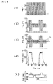
- Fig. 1 is a schematic diagram of a display panel provided by this invention.
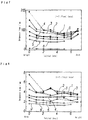
- Fig. 2 is a graph indicating (a) a relation between transmittance and voltage and (b) switching response characteristics of half-tone image (1 to 6 in (a)) of a bend cell having a cell gap of 6 ⁇ m.
- Fig. 3 is an illustrative diagram of three terminal element type AM drive LCD.
- Fig. 4 is a FET drive circuit diagram simulating AM-LCD using TFT.
- Fig. 5 is a schematic drawing illustrating the construction of a back light.
- Fig. 6 is an illustrative drawing of AM-LCD simulated experiments, were in (a) to (c) are gate a voltage Vg, drain voltage Vd and source voltage Vs, respectively, while (d) is a response curve for transmittance of the liquid crystal cell and (d) is an output of the back light.
- Fig. 7 is a graph indicating a response characteristic for switching half-tone images of a TN cell.
- Fig. 8 is a graph indicating a response characteristic for switching half-tone images in a bend cell having a cell gap of 8 ⁇ m.
- Fig. 1 is a schematic drawing provided in this invention.
- a phase compensation plate (phase difference plate) 3 is disposed in front of a bend orientation liquid crystal cell (bend cell) 1 in the display panel 10, the bend cell 1 and phase difference plate 3 being inserted between two cross polarizers 5, 5.
- a surface light source 7 for sequentially illuminating three color lights of red (R), green (G) and blue (B) is provided at the rear face of the display panel 10, wherein a drawing of a circuit for switching the color is omitted.
- the active matrix will be described hereinafter.
- Liquid crystal molecules are inclined into a reversed direction with each other on the surface of the top and bottom substrates 12 in the bend cell 1.
- the liquid crystal molecules may take either a bend orientation or a orientation having a twisted orientation at the center of the cell.
- the liquid crystal cell according to this invention is represented by a term "bend orientation liquid crystal cell (bend cell)" because two orientations described above are electro-optically almost identical with each other.
- liquid crystals having such orientation has a rapid response to orientational changes (i. e. change in transmittance) against voltage changes
- liquid crystals having a low viscosity for example LIXON TD-6004XX, TD-6001XX and TD-5068XX made by Chisso Co., were adopted in order to further increase the response speed for the purpose hitherto described, together with optimizing pre-tilt angles and phase compensation plates complying with the conditions above, as well as making cell gaps small.
- the cell gap has been determined to be 7 ⁇ m or more in the conventional art since smaller cell gaps tend to decrease the transmittance under the same driving voltage.
- cell gaps makes it difficult to attain a response speed of 3 ms or less.
- the lower limit of the cell gap is set to 1.5 ⁇ m for the present.
- the viscosity of the liquid crystal is 70 mPa ⁇ s or less, since a value of more than 70 mPa ⁇ s makes the response of the liquid crystal to be retarded.
- the pre-tilt angle is recommended to be set to 2 to 30° .
- the vias voltage V CR for allowing the liquid crystal to take a bend orientation becomes several volts or more resulting in a too high driving voltage while, when it is over 30 ° , retardation will be so small that transmittance of the liquid crystal cell would be lowered, both of which being not preferable results.
- the pre-tilt angle can be set within a preferable range of 0.1 to 30.0 ° .
- the optimum phase compensation plate is designed so that the orientation of liquid crystals under a low voltage (about 6V or less) is optically compensated.
- Refractive indices of the plate is set to be n Y > n X > n Z as shown in Fig. 1. However, these values may changed to be n Y > n Z > n X depending on physical parameters of the liquid crystal.
- Fig. 2 is a graph indicating (a) a relation between transmittance and voltage and (b) response characteristic of switching the half-tones image (1 to 6 in (a)) of a bend cell having a cell gap of 6 ⁇ m.
- a change from a low level to a high level in the half-tone images and a reversed change correspond to rise and decay time, respectively.
- the response time mainly depends on the final level of the half-tone image, that the response time is retarded at a low voltage, and that the object that the response time should be within about 3 ms as a whole is almost attained while it is a little slower than 3 ms in the worst conditions.
- a cross polarizer should be provided in order to visualize the changes in the orientation of liquid crystals in an electric field, those having an optical characteristics with little wave length dependency may be selected. It is desirable that, in constructing a LCD using a display panel according to this invention, an active matrix driving method frequently used in TN cells having color filters and being able to be applied for transmissive type with a high image quality is adopted in the driving method for exciting liquid crystals.
- Fig. 3 is an illustrative drawing of a three terminal element type AM drive LCD. Its basic structure shown in Fig. 3(a) comprises a substrate on which a three terminal element comprising a source, gate and drain is provided in a matrix, wherein a liquid crystal layer is disposed on tie three terminal element type matrix composed of a display electrode and capacitor connected to the source. A flat (common) electrode substrate without any pattern on it is usually used for the transparent counter electrode opposite to the substrate of the three terminal element type matrix electrode.
- the liquid crystal layer in Fig 3(a) corresponds to the liquid crystal 11 in Fig. 1 while tie display electrode 20 and transparent flat electrode 15 in Fig. 3(a) corresponds to the glass plate (substrate) 12 in Fig. 1.
- the phase compensation plate is disposed close to the front or rear face of the glass substrate, and the bottom face of the cross polarizer are disposed close to the front or rear face of the three terminal element matrix 19 while the top face of the cross polarizer is disposed close to the front face of the phase compensation plate or close to the front face of the glass substrate 12.
- the display panel is divided into image elements in an matrix array by the active matrix driving the panel.
- Fig. 3(b) The principle of operation of this kind of LCD is shown in Fig. 3(b).
- the three terminal elements on one gate bus is made into continuity (on) all at once, thereby supplying signal charges to all capacitors connected to these three terminal elements in a continuity state via signal array electrodes (drain bus, signal line) Y 1 , Y 2 , ..., Y n from a hold circuit in synchronize with this scanning (defined as refreshing (recording)).
- This signal charge continues to excite liquid crystals in all the image elements on the gate bus until subsequent scanning of the frame.
- a recording method called a "line at a time driving method” is illustrated in Fig. 3(b)
- a method called a "dotted sequential driving method” in which signals are sequentially recorded in each image element can be also adopted by providing a circuit corresponding to a scanning circuit connected to a gate bus instead of providing a hold circuit.
- the spare time before allowing the image elements on the scanning line at the bottom of the display to arrive at a desired half-tone image in the sequential color illumination method is one third of that in the micro-color filter method, it is inevitable that the recording time is made short.
- the orientation state will be unstable without attaining its saturated state by a usual single recording in a liquid crystal with relatively low purity and low resistivity, thereby sometimes deteriorating total image qualities. Such a problem could be avoided by two or more times of repeated recording.
- addressing device that allows two or more times of addressing into each image element during every illumination with each color. This will reduce the production cost since limitations on the purity of the liquid crystal are relaxed.
- Such a recording device can be easily constructed because it corresponds to a control circuit in which the scanning frequency of the scanning circuit in Fig. 3(b) is 1/N of the fold frequency of the hold circuit, provided that the recording times are N.
- ploysilicon which has a higher response speed than amorphous silicone widely used in conventional TN cells with color filters, as a material for TFT to be provided in the liquid crystal display according to this invention.
- the plane light source 7 was constructed so that R, G and B equally and sequentially illuminate the rear face of the bend cell 1 through a light guide plate 22 and scattering plate 13 from each cold cathod fluorescent lamp emitting each color of R, G and B as shown in Fig. 5.
- Fig. 6 is an illustrative drawing of the AM-LCD simulation experiment in which (a) to (c) are gate voltage Vg, drain voltage Vd and source voltage Vs. respectively, while (d) and (e) being a transmittance response curve of the liquid crystal cell and an output of a back light, respectively.
- the common voltage Vc was set to a constant value (about 7V).
- the response time for orientational changes of liquid crystal molecules is 1 to 3 ms, being very slow compared with the recording time of 2 ⁇ s per one scanning line as described above. Therefore, twice or more times of refresh before changing orientation to a required degree enables more accurate display of half-tone images.
- the voltage may be more largely changed than the voltage corresponding to the desired half-tone images, followed by impressing a prescribed half-tone voltage. Otherwise, refresh may be applied only one time by imposing a voltage determined by taking the electric capacity change accompanied by orientational changes into account.
- the voltage considering the changes of half-tone images as described above may not he applied when some discrepancy in half-tone images due to electric capacity change is ignored.
- one recording time becomes 3 ms and the recording time per one scanning line becomes 6 ⁇ s, since recording may be carried out within about one half of the display time per one color of 6 ms.
- the emission time of the light source is shortened, for example to 1 ms, so that the recording time for all display panel becomes 5 ms, enabling to take as long a time as 10 ⁇ s per one scanning time.
- polarity of Vd is inverted for every scanning line as in the example shown in Fig. 6. the polarity in one frame may be unchanged while inverting the polarity at the next frame.
- Fig. 6 illustrates an example where a voltage impression pattern was applied by changing only R.
- a liquid crystal shutter half-tone variable shutter
- corresponding to open (half-tone image 6) and close (half-tone image 1) are 6V and 2V, respectively, as shown in Fig. 6(c).
- transmittance of the liquid crystal rapidly responded to the impressed voltage attaining a response time of 3 ms in both rise and decay periods, thereby obtaining a clear monochromatic display of R.
- each synthesized color display can be obtained with a half-tone image of 6 by an experiment in which the shutter is made open for combined two or more of colors of R, G and B, and that each synthesized color display with a desired intensity can be obtained by an experiment in which an initial and final levels of the half-tone image are changed in many combinations other than a combination of open and close (half-tone image of 1 aid 6) for every combination among R, G and B.
Landscapes
- Physics & Mathematics (AREA)
- Engineering & Computer Science (AREA)
- General Physics & Mathematics (AREA)
- Crystallography & Structural Chemistry (AREA)
- Chemical & Material Sciences (AREA)
- Theoretical Computer Science (AREA)
- Computer Hardware Design (AREA)
- Nonlinear Science (AREA)
- Optics & Photonics (AREA)
- Mathematical Physics (AREA)
- Liquid Crystal (AREA)
- Liquid Crystal Display Device Control (AREA)
- Control Of Indicators Other Than Cathode Ray Tubes (AREA)
Applications Claiming Priority (3)
| Application Number | Priority Date | Filing Date | Title |
|---|---|---|---|
| JP11224697 | 1997-04-30 | ||
| JP11224697 | 1997-04-30 | ||
| JP112246/97 | 1997-04-30 |
Publications (3)
| Publication Number | Publication Date |
|---|---|
| EP0875880A2 true EP0875880A2 (de) | 1998-11-04 |
| EP0875880A3 EP0875880A3 (de) | 1998-11-11 |
| EP0875880B1 EP0875880B1 (de) | 2003-12-17 |
Family
ID=14581909
Family Applications (1)
| Application Number | Title | Priority Date | Filing Date |
|---|---|---|---|
| EP97116026A Expired - Lifetime EP0875880B1 (de) | 1997-04-30 | 1997-09-15 | Flüssigkristall-Anzeigevorrichtung mit feldsequentieller Farbwiedergabe |
Country Status (6)
| Country | Link |
|---|---|
| US (1) | US6108058A (de) |
| EP (1) | EP0875880B1 (de) |
| KR (1) | KR100303369B1 (de) |
| CN (1) | CN1121628C (de) |
| DE (1) | DE69726836T2 (de) |
| TW (1) | TW388001B (de) |
Cited By (9)
| Publication number | Priority date | Publication date | Assignee | Title |
|---|---|---|---|---|
| WO2004055774A1 (en) * | 2002-12-18 | 2004-07-01 | Koninklijke Philips Electronics N.V. | Scrolling backlight device for lcd display panel |
| WO2006006111A1 (en) * | 2004-07-07 | 2006-01-19 | Koninklijke Philips Electronics N.V. | Color display |
| WO2006052011A1 (en) * | 2004-11-11 | 2006-05-18 | Pentax Corporation | Color image pickup and display device |
| EP1331513A4 (de) * | 2000-10-17 | 2008-04-02 | Toshiba Matsushita Display Tec | Flüssigkristallanzeige und deren herstellungsverfahren |
| US7365729B2 (en) * | 2000-11-23 | 2008-04-29 | Lg.Philips Lcd Co., Ltd. | Field sequential LCD device and color image display method thereof |
| WO2008100493A1 (en) | 2007-02-15 | 2008-08-21 | Cree, Inc. | Partially filterless liquid crystal display devices and methods of operating the same |
| US7605786B2 (en) | 1999-03-26 | 2009-10-20 | Semiconductor Energy Laboratory Co., Ltd. | Liquid crystal display device |
| EP2293137A1 (de) * | 2009-08-07 | 2011-03-09 | Sony Corporation | Abblendvorrichtung basierend auf Flüssigkristallen und Bildanzeigesystem |
| US8836624B2 (en) | 2007-02-15 | 2014-09-16 | Cree, Inc. | Partially filterless and two-color subpixel liquid crystal display devices, mobile electronic devices including the same, and methods of operating the same |
Families Citing this family (27)
| Publication number | Priority date | Publication date | Assignee | Title |
|---|---|---|---|---|
| EP0997868B1 (de) * | 1998-10-30 | 2012-03-14 | Semiconductor Energy Laboratory Co., Ltd. | Rastersequentielle Flüssigkristall-Anzeige und ihr Steuerungsverfahren, und am Kopf montierte Anzeige Vorrichtung |
| KR100311210B1 (ko) * | 1998-12-29 | 2002-09-17 | 주식회사 하이닉스반도체 | 액정 표시 장치 |
| JP4637315B2 (ja) | 1999-02-24 | 2011-02-23 | 株式会社半導体エネルギー研究所 | 表示装置 |
| US7193594B1 (en) | 1999-03-18 | 2007-03-20 | Semiconductor Energy Laboratory Co., Ltd. | Display device |
| US6952194B1 (en) * | 1999-03-31 | 2005-10-04 | Semiconductor Energy Laboratory Co., Ltd. | Liquid crystal display device |
| KR100406742B1 (ko) * | 2000-11-22 | 2003-11-21 | 삼성에스디아이 주식회사 | 필드-시켄셜 디스플레이용 1-판넬 엘코스 엔진 |
| JP2003091019A (ja) * | 2001-09-19 | 2003-03-28 | Fujitsu Ltd | 液晶表示装置 |
| US20030080930A1 (en) * | 2001-10-31 | 2003-05-01 | Aiptek International Inc. | LCD device for showing multiple pictures |
| TWI351566B (en) | 2003-01-15 | 2011-11-01 | Semiconductor Energy Lab | Liquid crystal display device |
| JP4170121B2 (ja) * | 2003-03-20 | 2008-10-22 | 株式会社 日立ディスプレイズ | 液晶表示装置 |
| JP4225132B2 (ja) | 2003-06-24 | 2009-02-18 | カシオ計算機株式会社 | 液晶表示装置 |
| US7479309B2 (en) * | 2003-07-31 | 2009-01-20 | Nitto Denko Corporation | Multi-layered compensation film using specified Tg material as a birefringent layer |
| JP4471716B2 (ja) * | 2004-04-14 | 2010-06-02 | スタンレー電気株式会社 | カラー液晶表示装置及びその表示方法 |
| US7288296B2 (en) * | 2004-06-03 | 2007-10-30 | Nitto Denko Corporation | Multilayer optical compensator, liquid crystal display, and process |
| US20060097978A1 (en) * | 2004-10-22 | 2006-05-11 | Ng Kee Y | Field-sequential color display with feedback control |
| KR100691138B1 (ko) * | 2005-02-25 | 2007-03-09 | 엘지이노텍 주식회사 | 액정표시장치, 그 구동방법 및 이를 구비한 이동통신 단말기 |
| US7713595B2 (en) * | 2005-10-18 | 2010-05-11 | Nitto Denko Corporation | Optical compensation films produced by a carrier-web-casting process |
| US7480021B2 (en) * | 2005-12-29 | 2009-01-20 | Nitto Denko Corporation | Optical films having reverse dispersion |
| US20070247712A1 (en) * | 2006-04-21 | 2007-10-25 | Eastman Kodak Company | Optical elements having reverse dispersion |
| USRE45394E1 (en) | 2008-10-20 | 2015-03-03 | X6D Limited | 3D glasses |
| USD613328S1 (en) | 2009-05-13 | 2010-04-06 | X6D Ltd. | 3D glasses |
| USD624952S1 (en) | 2008-10-20 | 2010-10-05 | X6D Ltd. | 3D glasses |
| USD603445S1 (en) | 2009-03-13 | 2009-11-03 | X6D Limited | 3D glasses |
| CA2684513A1 (en) | 2008-11-17 | 2010-05-17 | X6D Limited | Improved performance 3d glasses |
| USD650956S1 (en) | 2009-05-13 | 2011-12-20 | X6D Limited | Cart for 3D glasses |
| TWI425480B (zh) * | 2009-12-24 | 2014-02-01 | Dynascan Technology Corp | A Display and Its Homogenization Method with Edge - Shaped Lightguide Combined Backlight |
| CN102956500A (zh) * | 2011-08-23 | 2013-03-06 | 广东中显科技有限公司 | 多晶硅薄膜晶体管的制备方法 |
Family Cites Families (8)
| Publication number | Priority date | Publication date | Assignee | Title |
|---|---|---|---|---|
| EP0138454B1 (de) * | 1983-09-26 | 1994-08-31 | Tektronix, Inc. | Schaltbarer Farbfilter und seine Verwendung in einer Anzeigevorrichtung mit sequentieller Rasterfolge und voller Farbwiedergabe |
| US4635051A (en) * | 1983-09-26 | 1987-01-06 | Tektronix, Inc. | High-speed electro-optical light gate and field sequential full color display system incorporating same |
| US4611889A (en) * | 1984-04-04 | 1986-09-16 | Tektronix, Inc. | Field sequential liquid crystal display with enhanced brightness |
| JP2565563B2 (ja) * | 1989-03-18 | 1996-12-18 | 株式会社日立製作所 | 液晶表示装置の製法および液晶表示装置用位相板の製法 |
| JP3233927B2 (ja) * | 1989-12-22 | 2001-12-04 | サーノフ コーポレイション | バツクライト液晶表示ピクセルアレイを用いたフイールド順次式表示システム及び画像生成方法 |
| JP2820336B2 (ja) * | 1991-10-22 | 1998-11-05 | シャープ株式会社 | アクティブマトリクス型液晶表示装置の駆動方法 |
| JPH0784254A (ja) * | 1993-09-18 | 1995-03-31 | Tatsuo Uchida | 広視野角・高速表示の液晶表示素子 |
| JP2974564B2 (ja) * | 1993-12-20 | 1999-11-10 | シャープ株式会社 | 液晶電子装置およびその駆動方法 |
-
1997
- 1997-09-11 US US08/927,687 patent/US6108058A/en not_active Expired - Lifetime
- 1997-09-13 KR KR1019970047398A patent/KR100303369B1/ko not_active Expired - Fee Related
- 1997-09-15 DE DE69726836T patent/DE69726836T2/de not_active Expired - Fee Related
- 1997-09-15 CN CN97122769A patent/CN1121628C/zh not_active Expired - Fee Related
- 1997-09-15 EP EP97116026A patent/EP0875880B1/de not_active Expired - Lifetime
- 1997-10-15 TW TW086115140A patent/TW388001B/zh not_active IP Right Cessation
Cited By (16)
| Publication number | Priority date | Publication date | Assignee | Title |
|---|---|---|---|---|
| US8125429B2 (en) | 1999-03-26 | 2012-02-28 | Semiconductor Energy Laboratory Co., Ltd. | Liquid crystal display device |
| US9704444B2 (en) | 1999-03-26 | 2017-07-11 | Semiconductor Energy Laboratory Co., Ltd. | Liquid crystal display device |
| US8896639B2 (en) | 1999-03-26 | 2014-11-25 | Semiconductor Energy Laboratory Co., Ltd. | Liquid crystal display device |
| US8149198B2 (en) | 1999-03-26 | 2012-04-03 | Semiconductor Energy Laboratory Co., Ltd. | Liquid crystal display device |
| US8144278B2 (en) | 1999-03-26 | 2012-03-27 | Semiconductor Energy Laboratory Co., Ltd. | Optically compensated birefringence mode liquid crystal display device |
| US7605786B2 (en) | 1999-03-26 | 2009-10-20 | Semiconductor Energy Laboratory Co., Ltd. | Liquid crystal display device |
| US7773066B2 (en) | 1999-03-26 | 2010-08-10 | Semiconductor Energy Laboratory Co., Ltd. | Liquid crystal display device |
| EP1331513A4 (de) * | 2000-10-17 | 2008-04-02 | Toshiba Matsushita Display Tec | Flüssigkristallanzeige und deren herstellungsverfahren |
| US7365729B2 (en) * | 2000-11-23 | 2008-04-29 | Lg.Philips Lcd Co., Ltd. | Field sequential LCD device and color image display method thereof |
| WO2004055774A1 (en) * | 2002-12-18 | 2004-07-01 | Koninklijke Philips Electronics N.V. | Scrolling backlight device for lcd display panel |
| WO2006006111A1 (en) * | 2004-07-07 | 2006-01-19 | Koninklijke Philips Electronics N.V. | Color display |
| WO2006052011A1 (en) * | 2004-11-11 | 2006-05-18 | Pentax Corporation | Color image pickup and display device |
| US7952544B2 (en) | 2007-02-15 | 2011-05-31 | Cree, Inc. | Partially filterless liquid crystal display devices and methods of operating the same |
| WO2008100493A1 (en) | 2007-02-15 | 2008-08-21 | Cree, Inc. | Partially filterless liquid crystal display devices and methods of operating the same |
| US8836624B2 (en) | 2007-02-15 | 2014-09-16 | Cree, Inc. | Partially filterless and two-color subpixel liquid crystal display devices, mobile electronic devices including the same, and methods of operating the same |
| EP2293137A1 (de) * | 2009-08-07 | 2011-03-09 | Sony Corporation | Abblendvorrichtung basierend auf Flüssigkristallen und Bildanzeigesystem |
Also Published As
| Publication number | Publication date |
|---|---|
| DE69726836D1 (de) | 2004-01-29 |
| TW388001B (en) | 2000-04-21 |
| CN1121628C (zh) | 2003-09-17 |
| KR100303369B1 (ko) | 2001-09-24 |
| EP0875880B1 (de) | 2003-12-17 |
| US6108058A (en) | 2000-08-22 |
| KR19980079366A (ko) | 1998-11-25 |
| DE69726836T2 (de) | 2004-11-04 |
| CN1197933A (zh) | 1998-11-04 |
| EP0875880A3 (de) | 1998-11-11 |
Similar Documents
| Publication | Publication Date | Title |
|---|---|---|
| EP0875880B1 (de) | Flüssigkristall-Anzeigevorrichtung mit feldsequentieller Farbwiedergabe | |
| US7532183B2 (en) | Liquid crystal display device and its drive method | |
| KR100725426B1 (ko) | 시분할 방식 액정표시장치 및 그의 컬러영상표시방법 | |
| KR100505924B1 (ko) | 액정표시장치 및 그 구동방법 | |
| US7268765B2 (en) | Method of color image display for a field sequential liquid crystal display device | |
| JPH09236798A (ja) | 液晶表示装置 | |
| US5745200A (en) | Color liquid crystal display device and liquid crystal display apparatus | |
| JP3592205B2 (ja) | 液晶表示装置の駆動方法 | |
| US5920301A (en) | Liquid crystal display apparatus using liquid crystal having ferroelectric phase and method of driving liquid crystal display device using liquid crystal having ferroelectric phase | |
| JP3504480B2 (ja) | 液晶ディスプレイ | |
| JP3804581B2 (ja) | 液晶表示装置の駆動方法 | |
| US7292220B2 (en) | Ferroelectric liquid crystal display and method of driving the same | |
| US20010035852A1 (en) | Display panel including liquid crystal material having spontaneous polarization | |
| KR100503430B1 (ko) | 액정표시장치 | |
| EP0679923B1 (de) | Flüssigkristall-Farbanzeigevorrichtung und Flüssigkristallanzeigegerät | |
| EP0686956A2 (de) | Flüssigkristallanzeigegerät mit ferroelektrischer Phase und Verfahren zu ihrer Steuerung | |
| KR101292149B1 (ko) | 액정표시장치 및 그의 구동방법 | |
| JP4212571B2 (ja) | 液晶表示装置及びその駆動方法 | |
| US6876424B1 (en) | Liquid crystal display having a spontaneous polarization | |
| JPH11133374A (ja) | カラー液晶表示装置の駆動方法 | |
| KR100701664B1 (ko) | 필드 시퀀셜 액정 표시 장치의 구동 방법 | |
| JP2000147548A (ja) | 液晶ディスプレイ | |
| JPH01182828A (ja) | 液晶表示パネル | |
| KR20040062156A (ko) | 액정표시장치 및 그 구동방법 | |
| KR20060062160A (ko) | 액정 표시 장치 |
Legal Events
| Date | Code | Title | Description |
|---|---|---|---|
| PUAI | Public reference made under article 153(3) epc to a published international application that has entered the european phase |
Free format text: ORIGINAL CODE: 0009012 |
|
| PUAL | Search report despatched |
Free format text: ORIGINAL CODE: 0009013 |
|
| 17P | Request for examination filed |
Effective date: 19971210 |
|
| AK | Designated contracting states |
Kind code of ref document: A2 Designated state(s): DE FR GB NL |
|
| AX | Request for extension of the european patent |
Free format text: AL;LT;LV;RO;SI |
|
| AK | Designated contracting states |
Kind code of ref document: A3 Designated state(s): AT BE CH DE DK ES FI FR GB GR IE IT LI LU MC NL PT SE |
|
| AX | Request for extension of the european patent |
Free format text: AL;LT;LV;RO;SI |
|
| AKX | Designation fees paid |
Free format text: DE FR GB NL |
|
| 17Q | First examination report despatched |
Effective date: 20000904 |
|
| GRAH | Despatch of communication of intention to grant a patent |
Free format text: ORIGINAL CODE: EPIDOS IGRA |
|
| GRAS | Grant fee paid |
Free format text: ORIGINAL CODE: EPIDOSNIGR3 |
|
| GRAA | (expected) grant |
Free format text: ORIGINAL CODE: 0009210 |
|
| AK | Designated contracting states |
Kind code of ref document: B1 Designated state(s): DE FR GB NL |
|
| REG | Reference to a national code |
Ref country code: GB Ref legal event code: FG4D |
|
| REF | Corresponds to: |
Ref document number: 69726836 Country of ref document: DE Date of ref document: 20040129 Kind code of ref document: P |
|
| ET | Fr: translation filed | ||
| PLBE | No opposition filed within time limit |
Free format text: ORIGINAL CODE: 0009261 |
|
| STAA | Information on the status of an ep patent application or granted ep patent |
Free format text: STATUS: NO OPPOSITION FILED WITHIN TIME LIMIT |
|
| 26N | No opposition filed |
Effective date: 20040920 |
|
| PGFP | Annual fee paid to national office [announced via postgrant information from national office to epo] |
Ref country code: NL Payment date: 20060918 Year of fee payment: 10 |
|
| PGFP | Annual fee paid to national office [announced via postgrant information from national office to epo] |
Ref country code: GB Payment date: 20060922 Year of fee payment: 10 Ref country code: FR Payment date: 20060922 Year of fee payment: 10 |
|
| PGFP | Annual fee paid to national office [announced via postgrant information from national office to epo] |
Ref country code: DE Payment date: 20061129 Year of fee payment: 10 |
|
| GBPC | Gb: european patent ceased through non-payment of renewal fee |
Effective date: 20070915 |
|
| PG25 | Lapsed in a contracting state [announced via postgrant information from national office to epo] |
Ref country code: NL Free format text: LAPSE BECAUSE OF NON-PAYMENT OF DUE FEES Effective date: 20080401 |
|
| NLV4 | Nl: lapsed or anulled due to non-payment of the annual fee |
Effective date: 20080401 |
|
| PG25 | Lapsed in a contracting state [announced via postgrant information from national office to epo] |
Ref country code: DE Free format text: LAPSE BECAUSE OF NON-PAYMENT OF DUE FEES Effective date: 20080401 |
|
| REG | Reference to a national code |
Ref country code: FR Ref legal event code: ST Effective date: 20080531 |
|
| PG25 | Lapsed in a contracting state [announced via postgrant information from national office to epo] |
Ref country code: FR Free format text: LAPSE BECAUSE OF NON-PAYMENT OF DUE FEES Effective date: 20071001 |
|
| PG25 | Lapsed in a contracting state [announced via postgrant information from national office to epo] |
Ref country code: GB Free format text: LAPSE BECAUSE OF NON-PAYMENT OF DUE FEES Effective date: 20070915 |