EP0871975B1 - Power segmented electrode - Google Patents
Power segmented electrode Download PDFInfo
- Publication number
- EP0871975B1 EP0871975B1 EP96922561A EP96922561A EP0871975B1 EP 0871975 B1 EP0871975 B1 EP 0871975B1 EP 96922561 A EP96922561 A EP 96922561A EP 96922561 A EP96922561 A EP 96922561A EP 0871975 B1 EP0871975 B1 EP 0871975B1
- Authority
- EP
- European Patent Office
- Prior art keywords
- electrode
- power
- electrodes
- semiconductor substrate
- plasma
- Prior art date
- Legal status (The legal status is an assumption and is not a legal conclusion. Google has not performed a legal analysis and makes no representation as to the accuracy of the status listed.)
- Expired - Lifetime
Links
Images

Classifications
-
- H—ELECTRICITY
- H01—ELECTRIC ELEMENTS
- H01J—ELECTRIC DISCHARGE TUBES OR DISCHARGE LAMPS
- H01J37/00—Discharge tubes with provision for introducing objects or material to be exposed to the discharge, e.g. for the purpose of examination or processing thereof
- H01J37/32—Gas-filled discharge tubes
- H01J37/32009—Arrangements for generation of plasma specially adapted for examination or treatment of objects, e.g. plasma sources
- H01J37/32082—Radio frequency generated discharge
-
- H—ELECTRICITY
- H01—ELECTRIC ELEMENTS
- H01J—ELECTRIC DISCHARGE TUBES OR DISCHARGE LAMPS
- H01J37/00—Discharge tubes with provision for introducing objects or material to be exposed to the discharge, e.g. for the purpose of examination or processing thereof
- H01J37/32—Gas-filled discharge tubes
- H01J37/32009—Arrangements for generation of plasma specially adapted for examination or treatment of objects, e.g. plasma sources
-
- H—ELECTRICITY
- H01—ELECTRIC ELEMENTS
- H01J—ELECTRIC DISCHARGE TUBES OR DISCHARGE LAMPS
- H01J37/00—Discharge tubes with provision for introducing objects or material to be exposed to the discharge, e.g. for the purpose of examination or processing thereof
- H01J37/32—Gas-filled discharge tubes
- H01J37/32431—Constructional details of the reactor
- H01J37/32532—Electrodes
-
- H—ELECTRICITY
- H01—ELECTRIC ELEMENTS
- H01J—ELECTRIC DISCHARGE TUBES OR DISCHARGE LAMPS
- H01J37/00—Discharge tubes with provision for introducing objects or material to be exposed to the discharge, e.g. for the purpose of examination or processing thereof
- H01J37/32—Gas-filled discharge tubes
- H01J37/32917—Plasma diagnostics
- H01J37/3299—Feedback systems
-
- H—ELECTRICITY
- H01—ELECTRIC ELEMENTS
- H01L—SEMICONDUCTOR DEVICES NOT COVERED BY CLASS H10
- H01L21/00—Processes or apparatus adapted for the manufacture or treatment of semiconductor or solid state devices or of parts thereof
- H01L21/67—Apparatus specially adapted for handling semiconductor or electric solid state devices during manufacture or treatment thereof; Apparatus specially adapted for handling wafers during manufacture or treatment of semiconductor or electric solid state devices or components ; Apparatus not specifically provided for elsewhere
- H01L21/683—Apparatus specially adapted for handling semiconductor or electric solid state devices during manufacture or treatment thereof; Apparatus specially adapted for handling wafers during manufacture or treatment of semiconductor or electric solid state devices or components ; Apparatus not specifically provided for elsewhere for supporting or gripping
- H01L21/6831—Apparatus specially adapted for handling semiconductor or electric solid state devices during manufacture or treatment thereof; Apparatus specially adapted for handling wafers during manufacture or treatment of semiconductor or electric solid state devices or components ; Apparatus not specifically provided for elsewhere for supporting or gripping using electrostatic chucks
Definitions
- the invention relates to an electrode for generating a plasma and/or local plasma density control in a plasma reaction chamber.
- the electrode can be incorporated in an upper electrode and/or incorporated in a substrate support such as a chucking device for holding a substrate such as a semiconductor wafer, flat panel display, etc., during processing thereof in a plasma gas environment.
- Equipment for processing semiconductor wafers in a plasma gas environment typically couple radio frequency (RF) power from the plasma gas to the wafer to effect surface treatment of the wafer (e.g., etching, deposition, etc).
- RF radio frequency
- U.S. Patent No. 4,617,079 discloses a parallel plate arrangement wherein a wafer is supported on a lower electrode, RF power from a low frequency generator passes through a low frequency network, RF power from a high frequency generator is combined with the low frequency RF power in a high frequency matching and combining network, and the combined signals are applied across upper and lower electrodes.
- the high frequency matching and combining circuit can include a high frequency trap (capacitor and inductor in parallel) tuned to the frequency of the high frequency source for preventing signals generated by the high frequency source from being fed back to the low frequency source but allowing signals generated by the low frequency source to pass therethrough without being attenuated.
- a high frequency trap capacitor and inductor in parallel
- U.S. Patent No. 4,948,458 discloses a parallel plate arrangement wherein the upper electrode is in the form of an electrically conductive coil located outside the plasma reaction chamber and by inducing an RF current in the coil a magnetic field is produced in a planar region parallel to the plane of the coil.
- the coil is driven by an RF generator which supplies power to a matching circuit having a primary coil and a secondary loop.
- a variable capacitor in series with the secondary loop adjusts the circuit resonant frequency with the frequency output of the RF generator and impedance matching maximizes efficiency of power transfer to the planar coil.
- An additional capacitor in the primary circuit cancels parts of the inductive reactance of the coil in the circuit.
- European Patent No. 0280074 discloses an electrode structure having a number of electrode sub-units attached to it. The electrode is mounted above a sample holder in a plasma reactor chamber.
- IBM Technical Disclosure Bulletin VoL 28, No. 1, pages 259-260, entitled “Electrode Arrangement for Plasma Etching” describes an electrode divided into four sections, useful for plasma etching through holes in printed circuit boards.
- WO 96/18207 published after the priority date of this invention teaches a power segmented electrode comprising a concentric arrangement of electrodes separated by a dielectric gap, the electrodes connected in parallel to an RF power supply.
- the invention provides a power segmented electrode attachable to a plasma reaction chamber and capable of providing uniform processing of a semiconductor substrate in a plasma reaction chamber, comprising: first and second electrodes, the first electrode being distributed across a first zone and the second electrode being distributed across a second zone and a capacitive network controlling distribution of radio frequency power in the first and second zones, such that plasma coupled to a semiconductor substrate supported in the plasma reaction chamber provides uniform processing across the semiconductor substrate.
- the power segmented electrode is incorporated in a substrate support which supports a single semiconductor substrate in the plasma reaction chamber and the substrate support is an electrostatic chuck which clamps the semiconductor substrate.
- references to the substrate support are to a substrate support including or acting as an electrostatic chuck.
- the power segmented electrode can be embodied in various ways.
- the first electrode can be separated from the second electrode by a gap filled with dielectric material to form an interelectrode capacitor of the capacitive network.
- the first electrode may surround the second electrode, being separated from the second electrode by the gap.
- the first and second electrodes may form part of a concentric electrode arrangement composed of a plurality of spaced apart annular electrodes. Adjacent ones of the plurality of electrodes are separated by gaps, and each of the gaps can be filled with dielectric material to form interelectrode capacitors of the capacititve network.
- the plurality of electrodes can be provided in a pattern which compensates for process gas flow in the reaction chamber and provide uniform processing of the substrate.
- First and second capacitors can form part of the capacitive network and radio frequency power from a power source can pass sequentially through the first capacitor, through the first electrode, through the second capacitor, through the second electrode and to an electrical ground.
- the capacitive network can comprise first and second capacitors, the first capacitor being connected to the first electrode and the second capacitor being connected to the second electrode, the first and second capacitors being electrically connected in parallel to a radio frequency power source.
- the power segmented electrode can include a third electrode, the first electrode surrounding the second electrode and the second electrode surrounding the third electrode, each of the electrodes being electrically connected to a radio frequency power source, radio frequency power from the power source passing sequentially through a power splitter and to a respective one of the electrodes.
- the electrodes can be electrically connected to a radio frequency power source through variable capacitors forming part of the capacitive network and radio frequency power from the power source sequentially passing through each of the variable capacitors and to a respective one of the electrodes.
- current sensing mechanisms can be provided for automatically adjusting capacitance of a respective one of the variable capacitors such that adjustment signals emitted therefrom compensate for deviations from uniformity of processing of the substrate in an annular zone of the substrate facing a respective one ofthe annular electrodes.
- the first and second electrodes can be electrically connected to direct current biasing sources which allow the chuck to electrostatically clamp a substrate on the chuck.
- the radio frequency power can be supplied in phase or out of phase to the first and second electrodes.
- a passive network may be used for supplying power and DC bias to the first and second electrodes.
- the power segmented electrode can further include a sine wave generator for generating a numerically sequenced sine wave, a biasing unit for generating a DC offset value, a summation unit for summing the numerically sequenced sine wave and the DC offset value, a digital/analog converter for converting the signal output from the summation unit to an analog summation signal, a low pass filter for filtering predetermined low frequency portions of the analog summation signal, and a power amplifier for amplifying the analog summation signal filtered by the low pass filter and driving the first and second electrodes with the amplified signal.
- a sine wave generator for generating a numerically sequenced sine wave
- a biasing unit for generating a DC offset value
- a summation unit for summing the numerically sequenced sine wave and the DC offset value
- a digital/analog converter for converting the signal output from the summation unit to an analog summation signal
- a low pass filter for filtering predetermined low frequency portions of the analog sum
- the capacitive network can supply more power to the second electrode than to the first electrode where the first electrode surrounds the second electrode power can be supplied to the first and second electrodes by sequentially passing through the first electrode, an interelectrode capacitor formed by a dielectric material disposed in a gap between the first and second electrodes, the second electrode, a series of capacitors forming part of the capacitive network and an electrical ground, the dielectric material providing the interelectrode capacitance to be less than that of the series of capacitors.
- the power segmented electrode can further comprise a voltage divider circuit electrically connected to the first electrode or the second electrode.
- the first electrode can be driven by a first active power driver and the second electrode can be driven by a second active power driver, the first and second power drivers being operated independently of each other.
- the invention provides a method for processing a semiconductor substrate in a plasma processing chamber, comprising the steps of; electrostatically clamping a semiconductor substrate on a substrate support in a plasma reaction chamber, wherein the substrate support is an electrostatic chuck; generating plasma in the plasma reaction chamber with a power segmented electrode having a plurality of electrodes associated with zones of the semiconductor substrate, the power segmented electrode being incorporated in the substrate support; and controlling the distribution of power supplied to the electrodes so that uniform processing is applied across the semiconductor substrate to be processed, the power being distributed to the zones of the semiconductor substrate by a capacitive network connected to a plurality of electrodes.
- the invention provides a power segmented electrode of a plasma reaction chamber wherein density of the plasma can be locally enhanced or weakened to achieve desired substrate processing conditions.
- density of the plasma can be locally enhanced or weakened to achieve desired substrate processing conditions.
- it is typically desired to achieve uniform processing of the exposed surface of the wafer from center to edge thereof.
- localized control of the plasma density is achieved with a capacitive network which balances RF power such that plasma coupled to the wafer in zones adjacent the exposed surface of the wafer provides uniform wafer processing, e.g., during etching a layer on the wafer or building up a layer on the wafer.
- the power segmented electrode is incorporated in an electrostatic chucking arrangement for holding a substrate such as a semiconductor wafer during processing thereof.
- the electrostatic chuck can comprise a bipolar chuck or other type of electrode arrangement.
- the power segmented electrode of the invention can provide local plasma density control and thus achieve substantial improvement in uniformity compared to previously known electrode arrangements.
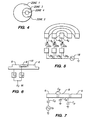
- the power segmented electrode is incorporated in a bipolar chuck, as shown in FIG. 1(a).
- the power segmented electrode includes three or more electrodes, as shown in FIG. 2.
- the electrodes of the power segmented electrode are arranged in a series and supplied RF power by a single RF power supply, as shown in FIG. 1(a).
- the electrodes are arranged in parallel and supplied RF power by a single RF power supply, as shown in FIG. 5.
- the RF power can be passed through individual variable capacitors, as shown in FIG. 5, or through a power splitter, as shown in FIG. 2.
- the electrodes can be electrically connected to current sensors and/or variable capacitors, as shown in FIG. 5.
- a substrate S in the form of a semiconductor wafer is supported on a substrate support 2 in the form of a wafer chuck system located in a plasma reaction chamber of a plasma reactor.
- the chuck system includes electrodes 4 which can be used to locally vary the amount of coupling of plasma to the wafer.
- the electrodes 4 include a first electrode 6 surrounding a second electrode 8, the first electrode 6 being located in a first zone 10 of the substrate support 2 and the second electrode being located in a second zone 12 of the substrate support 2.
- the chuck system also includes an RF power source 16 which supplies balanced RF power in the first and second zones 10 and 12.
- power from the RF power source 16 passes through the first electrode 6, through a gap 18 to the second electrode 8 and then to ground 20.
- the gap 18 is preferably filled with a dielectric material and the size of the gap 18 is chosen to provide an interelectrode capacitance effective in balancing the RF power between the first and second electrodes 6 and 8 such that plasma coupled to the wafer in the first and second zones 10 and 12 provides uniform processing from center to edge of the wafer.
- FIG. 1(b) illustrates an electrical schematic diagram of this ESC wafer clamping system.
- a source capacitance C d is connected at the input to smooth the power applied to the first electrode 6 and the inherent capacitance between the second electrode 8 and ground is represented by C b .
- the ratio between the capacitance of gap 18 (represented by C g ) and the base capacitance C b determines the voltage applied to the first and second electrodes 6 and 8.
- the capacitors in this schematic diagram can be chosen to match the voltage requirements at each zone based on known RF phase and matching requirements. Thereby, the capacitor values are chosen to tailor the fields as desired to achieve plasma processing uniformity.
- FIG. 2 illustrates another embodiment of the invention wherein an electrode is segmented into a plurality of concentric annular rings.
- FIG. 2 illustrates the electrode 4 segmented into first, second, and third concentric annular rings 4a, 4b, and 4c for allowing independent RF bias power zones which control the center-to-edge surface uniformity of the wafer.
- the electrode 4 is segmented into three zones.
- any number of concentric annular rings may be used for separating the electrode into zones in order to achieve the desired surface uniformity.
- the power source 16 may be connected to a power splitter 26 as illustrated in FIG. 2 for controlling the energy applied to each of the zones. Also.
- FIG. 2 illustrates another embodiment of the invention wherein an electrode is segmented into a plurality of concentric annular rings.
- FIG. 2 illustrates the electrode 4 segmented into first, second, and third concentric annular rings 4a, 4b, and 4c for allowing independent RF bias power zones which control the center-to-edge surface uniformity of
- FIG. 2 illustrates a DC bias source 28 connected to the concentric annular rings of the electrode for providing electrostatic clamping of the wafer.
- the annular zoned electrode controls the power applied to the surface of the wafer so that a symmetrical center-to-edge plasma processing is produced.
- the RF power and the DC bias delivered to each concentric annular ring of the first electrode 6 can be achieved in a conventional manner by a passive network in conjunction with RF generators and high voltage power supplies.
- the segments of the electrodes can also be driven by a numerically sequenced sine wave combined with a DC offset value as illustrated in FIG. 3.
- the sequenced sine wave is stored in a ROM 50 and the DC offset value is generated by a voltage source 52 in the embodiment illustrated in FIG. 3.
- the outputs of the ROM 50 and the voltage generator 52 are summed by a summing circuit 54 and then input to a digital-to-analog converter 56 which outputs an analog signal.
- the analog signal output from the digital-to-analog converter 56 is low pass filtered by a low pass filter 58 and then the filtered signal output is amplified by a power amplifier 60 and applied to the segmented electrodes 4a, 4b, and 4c.
- the electrodes may also be segmented into other patterns as desired to achieve processing uniformity requirements, and FIG. 4 illustrates another embodiment where an asymmetrical pattern of segmented electrodes is used. In the embodiment illustrated in FIG. 4, the electrode is segmented into four zones. However, the electrodes can be designed to provide a pattern which compensates for the chamber geometry, gas delivery, or asymmetrical pumping of the plasma processing system.
- FIG. 5 illustrates another embodiment of the invention wherein an active mechanism is used to control the power delivered to different zones of electrodes.
- FIG. 5 illustrates a plurality of current sensors 24 and a plurality of variable capacitors 22 connected to the segmented electrodes.
- the current sensors 24 provide active control of the variable capacitors 22. This active mechanism is used to control the percentage of power sent to the electrode zones by a feedback loop through the current sensors 24 to the variable capacitors 22.
- FIG. 6 illustrates another embodiment of the invention where two variable capacitors C1 and C2 are used to simultaneously couple RF energy into both poles of an ESC wafer clamping system. This embodiment helps to prevent any phase shift and charge imbalance across the portions of the chuck.
- FIG. 7 illustrates another embodiment of the invention where a voltage divider circuit and a capacitor network balance and adjust the RF voltage applied to the chuck surface.
- a parallel capacitance C p to the base capacitance is varied to set up the voltage divider.
- the capacitance value is selected by running uniformity tests on patterned and unpatterned oxide wafers and comparing the numerical data and diameter scans for result verification.
- wafer process uniformity i.e., center-to-edge
- the power segmented electrode according to the invention provides significant improvement in that wafer process uniformities of 1.5% or even lower can be achieved.
Landscapes
- Engineering & Computer Science (AREA)
- Physics & Mathematics (AREA)
- Plasma & Fusion (AREA)
- Chemical & Material Sciences (AREA)
- Analytical Chemistry (AREA)
- Computer Hardware Design (AREA)
- General Physics & Mathematics (AREA)
- Manufacturing & Machinery (AREA)
- Condensed Matter Physics & Semiconductors (AREA)
- Microelectronics & Electronic Packaging (AREA)
- Power Engineering (AREA)
- Drying Of Semiconductors (AREA)
- Container, Conveyance, Adherence, Positioning, Of Wafer (AREA)
- Plasma Technology (AREA)
- Inert Electrodes (AREA)
- Primary Cells (AREA)
- Surgical Instruments (AREA)
- Cable Accessories (AREA)
Abstract
Description
electrode, the first and second capacitors being electrically connected in parallel to a radio frequency power source. The power segmented electrode can include a third electrode, the first electrode surrounding the second electrode and the second electrode surrounding the third electrode, each of the electrodes being electrically connected to a radio frequency power source, radio frequency power from the power source passing sequentially through a power splitter and to a respective one of the electrodes.
Claims (17)
- A power segmented electrode attachable to a plasma reaction chamber and capable of providing uniform processing of a semiconductor substrate in the plasma reaction chamber, comprising:characterized in that the power segmented electrode is incorporated in a substrate support (2) which supports a single semiconductor substrate in the plasma reaction chamber and the substrate support (2) is an electrostatic chuck which clamps the semiconductor substrate.first and second electrodes (4,6,8), the first electrode being distributed across a first zone (10) and the second electrode being distributed across a second zone (12); anda capacitive network (Cd, Cg, Cb, Cp, C1, C2, 18, 22) controlling distribution of radio frequency power in the first and second zones (10,12), such that plasma coupled to a semiconductor substrate supported in the plasma reaction chamber provides uniform processing across the semiconductor substrate;
- The power segmented electrode of claim 1, wherein the substrate support (2) supports a single semiconductor wafer and the substrate support (2) is located in a plasma etching chamber.
- The power segmented electrode of claim 1, wherein the first electrode (6) is separated from the second electrode (8) by a gap (18), the gap (18) being filled with dielectric material and forming an interelectrode capacitor of the capacitive network.
- The power segmented electrode of claim 1, further comprising a radio frequency power source (16), first and second capacitors (Cd, Cg) forming part of the capacitive network and an electrical ground, radio frequency power from the power source (16) passing sequentially through the first capacitor (Cd), through the first electrode (6), through the second capacitor (Cg), through the second electrode (8), and to the electrical ground.
- The power segmented electrode of claim 1, wherein the first and second electrodes (4, 6, 8) form part of a concentric electrode arrangement comprising a plurality of spaced apart annular electrodes (4a, 4b, 4c), the electrodes (4a, 4b, 4c) being electrically connected to a radio frequency power source (16) through variable capacitors (22a, 22b, 22c) forming part of the capacitive network and radio frequency power from the power source (16) sequentially passing through each of the variable capacitors (22a, 22b, 22c) and to a respective one of the electrodes (4a, 4b, 4c).
- The power segmented electrode of claim 5, further comprising current sensing mechanisms (24a, 24b, 24c) for automatically adjusting capacitance of a respective one of the variable capacitors (22a, 22b, 22c) such that adjustment signals emitted therefrom compensate for deviations from uniformity of processing of the semiconductor substrate in an annular zone of the semiconductor substrate facing a respective one ofthe annular electrodes (4a, 4b, 4c).
- The power segmented electrode of claim 1, wherein the capacitive network comprises first and second capacitors (C1, C2), the first capacitor (C1) being connected to the first electrode (6) and the second capacitor (C2) being connected to the second electrode (8), the first and second capacitors (C1, C2) being electrically connected in parallel to a radio frequency power source (16).
- The power segmented electrode of claim 1, further comprising a third electrode (4a), the first electrode (4c) surrounding the second electrode (4b) and the second electrode (4b) surrounding the third electrode (4a), each of the electrodes (4a, 4b, 4c) being electrically connected to a radio frequency power source (16), radio frequency power from the power source (16) passing sequentially through a power splitter (26) and to a respective one of the electrodes (4a, 4b, 4c).
- The power segmented electrode of claim 1, wherein the first and second electrodes (4a, 4b, 4c) are electrically connected to direct current biasing sources (28) which allow the electrostatic chuck to electrostatically clamp the semiconductor substrate on the electrostatic chuck.
- The power segmented electrode of claim 1, further comprising a source of radio frequency power (16) supplied in phase or out of phase to the first and second electrodes (4, 6, 8).
- The power segmented electrode of claim 1, further comprising:a sine wave generator (50) for generating a numerically sequenced sine wave;a biasing unit (52) for generating a DC offset value;a summation unit (54) for summing the numerically sequenced sine wave and the DC offset value;a digital/analog converter (56) for converting the signal output from the summation unit (54) to an analog summation signal;a low pass filter (58) for filtering predetermined low frequency portions of the analog summation signal; anda power amplifier (60) for amplifying the analog summation signal filtered by the low pass filter and driving the first and second electrodes (4, 6, 8) with the amplified signal.
- The power segmented electrode of claim 1, wherein the first electrode (6) surrounds the second electrode (8) and power is supplied to the first and second electrodes (6, 8) by sequentially passing through the first electrode (6), an interelectrode capacitor (Cg) formed by a dielectric material disposed in a gap (18) between the first and second electrodes (6, 8), the second electrode (8), a series of capacitors (Cp, Cb) forming part of the capacitive network and an electrical ground, the dielectric material providing the interelectrode capacitance (Cg) to be less than that of the series of capacitors ( Cp, Cb).
- The power segmented electrode of claim 1, further comprising a voltage divider circuit (Cb, Cp) electrically connected to the first electrode (6) or the second electrode (8).
- The power segmented electrode of claim 1, wherein the first electrode (4a, 4b, 4c) is driven by a first active power driver (22, 24) and the second electrode (4a, 4b, 4c) is driven by a second active power driver (22, 24), the first and second power drivers (22,24) being operated independently of each other.
- A method for processing a semiconductor substrate in a plasma processing chamber, comprising the steps of:(a) electrostatically clamping a semiconductor substrate on a substrate support (2) in a plasma reaction chamber, wherein the substrate support is an electrostatic chuck;(b) generating plasma in the plasma reaction chamber with a power. segmented electrode having a plurality of electrodes (4, 6, 8) associated with zones of the semiconductor substrate, the power segmented electrode being incorporated in the substrate support; and(c) controlling distribution of power supplied to the electrodes (4, 6, 8) so that uniform processing is applied across the semiconductor substrate to be processed, the power being distributed to the zones of the semiconductor substrate, by a capacitive network (Cd, Cg, Cb, Cp, C1, C2, 18, 22) connected to the plurality of electrodes (4, 6, 8).
- The method according to claim 15, wherein the plurality of electrodes (4, 6, 8) are provided in a pattern which compensates for process gas flow in the plasma reaction chamber and provide uniform processing across the semiconductor substrate.
- The method according to claim 15, wherein the plasma reaction chamber is a plasma etching chamber and the semiconductor substrate is etched by the plasma.
Applications Claiming Priority (3)
| Application Number | Priority Date | Filing Date | Title |
|---|---|---|---|
| US08/491,349 US6042686A (en) | 1995-06-30 | 1995-06-30 | Power segmented electrode |
| US491349 | 1995-06-30 | ||
| PCT/US1996/010805 WO1997002589A1 (en) | 1995-06-30 | 1996-06-20 | Power segmented electrode |
Publications (2)
| Publication Number | Publication Date |
|---|---|
| EP0871975A1 EP0871975A1 (en) | 1998-10-21 |
| EP0871975B1 true EP0871975B1 (en) | 2003-08-20 |
Family
ID=23951816
Family Applications (1)
| Application Number | Title | Priority Date | Filing Date |
|---|---|---|---|
| EP96922561A Expired - Lifetime EP0871975B1 (en) | 1995-06-30 | 1996-06-20 | Power segmented electrode |
Country Status (8)
| Country | Link |
|---|---|
| US (2) | US6042686A (en) |
| EP (1) | EP0871975B1 (en) |
| JP (1) | JP4026727B2 (en) |
| KR (3) | KR100479201B1 (en) |
| AT (1) | ATE247866T1 (en) |
| AU (1) | AU6339196A (en) |
| DE (1) | DE69629588T2 (en) |
| WO (1) | WO1997002589A1 (en) |
Cited By (2)
| Publication number | Priority date | Publication date | Assignee | Title |
|---|---|---|---|---|
| WO2021055763A1 (en) * | 2019-09-19 | 2021-03-25 | Applied Materials, Inc. | In-situ dc plasma for cleaning pedestal heater |
| WO2024076410A1 (en) * | 2022-10-06 | 2024-04-11 | Tokyo Electron Limited | System and method for plasma process uniformity control |
Families Citing this family (131)
| Publication number | Priority date | Publication date | Assignee | Title |
|---|---|---|---|---|
| DE19814871A1 (en) * | 1998-04-02 | 1999-10-07 | Max Planck Gesellschaft | Method and device for targeted particle manipulation and deposition |
| KR100292411B1 (en) * | 1998-09-25 | 2001-06-01 | 윤종용 | Plasma apparatus for fabricating semiconductor device |
| US6492612B1 (en) * | 1998-12-28 | 2002-12-10 | Tokyo Electron Limited | Plasma apparatus and lower electrode thereof |
| US6367413B1 (en) * | 1999-06-15 | 2002-04-09 | Tokyo Electron Limited | Apparatus for monitoring substrate biasing during plasma processing of a substrate |
| JP2001035808A (en) * | 1999-07-22 | 2001-02-09 | Semiconductor Energy Lab Co Ltd | Wiring and its creating method, semiconductor device having this wiring, and dry-etching method therefor |
| JP4585648B2 (en) * | 1999-09-03 | 2010-11-24 | 株式会社アルバック | Plasma processing equipment |
| US8114245B2 (en) * | 1999-11-26 | 2012-02-14 | Tadahiro Ohmi | Plasma etching device |
| US6363882B1 (en) * | 1999-12-30 | 2002-04-02 | Lam Research Corporation | Lower electrode design for higher uniformity |
| WO2001052302A1 (en) * | 2000-01-10 | 2001-07-19 | Tokyo Electron Limited | Segmented electrode assembly and method for plasma processing |
| US20030079983A1 (en) * | 2000-02-25 | 2003-05-01 | Maolin Long | Multi-zone RF electrode for field/plasma uniformity control in capacitive plasma sources |
| WO2001063642A1 (en) * | 2000-02-25 | 2001-08-30 | Tokyo Electron Limited | Multi-zone rf electrode for capacitive plasma sources |
| JP4655385B2 (en) * | 2000-03-01 | 2011-03-23 | 株式会社日立製作所 | Plasma processing apparatus and processing method |
| WO2001073814A2 (en) | 2000-03-28 | 2001-10-04 | Tokyo Electron Limited | Method and apparatus for controlling power delivered to a multiple segment electrode |
| TWI224806B (en) | 2000-05-12 | 2004-12-01 | Semiconductor Energy Lab | Semiconductor device and manufacturing method thereof |
| WO2002013225A2 (en) * | 2000-08-08 | 2002-02-14 | Tokyo Electron Limited | Plasma processing method and apparatus |
| TW478026B (en) * | 2000-08-25 | 2002-03-01 | Hitachi Ltd | Apparatus and method for plasma processing high-speed semiconductor circuits with increased yield |
| TW529085B (en) * | 2000-09-22 | 2003-04-21 | Alps Electric Co Ltd | Method for evaluating performance of plasma treatment apparatus or performance confirming system of plasma treatment system |
| JP4717295B2 (en) * | 2000-10-04 | 2011-07-06 | 株式会社半導体エネルギー研究所 | Dry etching apparatus and etching method |
| TW519716B (en) * | 2000-12-19 | 2003-02-01 | Tokyo Electron Ltd | Wafer bias drive for a plasma source |
| US6741446B2 (en) * | 2001-03-30 | 2004-05-25 | Lam Research Corporation | Vacuum plasma processor and method of operating same |
| US20060191637A1 (en) * | 2001-06-21 | 2006-08-31 | John Zajac | Etching Apparatus and Process with Thickness and Uniformity Control |
| US20050059250A1 (en) * | 2001-06-21 | 2005-03-17 | Savas Stephen Edward | Fast etching system and process for organic materials |
| US6838387B1 (en) | 2001-06-21 | 2005-01-04 | John Zajac | Fast etching system and process |
| JP2003045874A (en) | 2001-07-27 | 2003-02-14 | Semiconductor Energy Lab Co Ltd | Metallized wiring and its forming method, metallized wiring board and its producing method |
| US6642661B2 (en) * | 2001-08-28 | 2003-11-04 | Tokyo Electron Limited | Method to affect spatial distribution of harmonic generation in a capacitive discharge reactor |
| TW591714B (en) * | 2002-02-20 | 2004-06-11 | Radiiontech Co Ltd | Cleaning apparatus using atmospheric pressure plasma |
| JP4753276B2 (en) * | 2002-11-26 | 2011-08-24 | 東京エレクトロン株式会社 | Plasma processing method and plasma processing apparatus |
| TW201041455A (en) * | 2002-12-16 | 2010-11-16 | Japan Science & Tech Agency | Plasma generation device, plasma control method, and substrate manufacturing method |
| KR100528464B1 (en) * | 2003-02-06 | 2005-11-15 | 삼성전자주식회사 | Security system of smart card |
| US7075771B2 (en) * | 2003-05-21 | 2006-07-11 | Tokyo Electron Limited | Apparatus and methods for compensating plasma sheath non-uniformities at the substrate in a plasma processing system |
| US20050031796A1 (en) * | 2003-08-07 | 2005-02-10 | Taiwan Semiconductor Manufacturing Co., Ltd. | Method and apparatus for controlling spatial distribution of RF power and plasma density |
| US7426900B2 (en) * | 2003-11-19 | 2008-09-23 | Tokyo Electron Limited | Integrated electrostatic inductive coupling for plasma processing |
| US7771562B2 (en) * | 2003-11-19 | 2010-08-10 | Tokyo Electron Limited | Etch system with integrated inductive coupling |
| US20050130620A1 (en) * | 2003-12-16 | 2005-06-16 | Andreas Fischer | Segmented radio frequency electrode apparatus and method for uniformity control |
| KR100622831B1 (en) * | 2004-04-13 | 2006-09-18 | 주식회사 에이디피엔지니어링 | Apparatus for processing substrate using plasma |
| US7276135B2 (en) * | 2004-05-28 | 2007-10-02 | Lam Research Corporation | Vacuum plasma processor including control in response to DC bias voltage |
| US20060021580A1 (en) * | 2004-06-02 | 2006-02-02 | Tokyo Electron Limited | Plasma processing apparatus and impedance adjustment method |
| US7988816B2 (en) | 2004-06-21 | 2011-08-02 | Tokyo Electron Limited | Plasma processing apparatus and method |
| US7951262B2 (en) | 2004-06-21 | 2011-05-31 | Tokyo Electron Limited | Plasma processing apparatus and method |
| JP4550507B2 (en) * | 2004-07-26 | 2010-09-22 | 株式会社日立ハイテクノロジーズ | Plasma processing equipment |
| US20060037704A1 (en) * | 2004-07-30 | 2006-02-23 | Tokyo Electron Limited | Plasma Processing apparatus and method |
| KR100663351B1 (en) * | 2004-11-12 | 2007-01-02 | 삼성전자주식회사 | Plasma processing apparatus |
| JP4642528B2 (en) * | 2005-03-31 | 2011-03-02 | 東京エレクトロン株式会社 | Plasma processing apparatus and plasma processing method |
| JP4704088B2 (en) | 2005-03-31 | 2011-06-15 | 東京エレクトロン株式会社 | Plasma processing equipment |
| US7993489B2 (en) | 2005-03-31 | 2011-08-09 | Tokyo Electron Limited | Capacitive coupling plasma processing apparatus and method for using the same |
| JP5004436B2 (en) * | 2005-05-23 | 2012-08-22 | 東京エレクトロン株式会社 | Electrostatic adsorption electrode and processing device |
| US7851368B2 (en) * | 2005-06-28 | 2010-12-14 | Lam Research Corporation | Methods and apparatus for igniting a low pressure plasma |
| US20070029193A1 (en) * | 2005-08-03 | 2007-02-08 | Tokyo Electron Limited | Segmented biased peripheral electrode in plasma processing method and apparatus |
| US20070044914A1 (en) * | 2005-08-30 | 2007-03-01 | Katsuji Matano | Vacuum processing apparatus |
| JP4801522B2 (en) * | 2006-07-21 | 2011-10-26 | 株式会社日立ハイテクノロジーズ | Semiconductor manufacturing apparatus and plasma processing method |
| US7749398B2 (en) * | 2006-09-29 | 2010-07-06 | Tokyo Electron Limited | Selective-redeposition sources for calibrating a plasma process |
| US7776748B2 (en) * | 2006-09-29 | 2010-08-17 | Tokyo Electron Limited | Selective-redeposition structures for calibrating a plasma process |
| US8017029B2 (en) | 2006-10-30 | 2011-09-13 | Applied Materials, Inc. | Plasma mask etch method of controlling a reactor tunable element in accordance with the output of an array of optical sensors viewing the mask backside |
| US20080099437A1 (en) * | 2006-10-30 | 2008-05-01 | Richard Lewington | Plasma reactor for processing a transparent workpiece with backside process endpoint detection |
| US7967930B2 (en) | 2006-10-30 | 2011-06-28 | Applied Materials, Inc. | Plasma reactor for processing a workpiece and having a tunable cathode |
| US8012366B2 (en) | 2006-10-30 | 2011-09-06 | Applied Materials, Inc. | Process for etching a transparent workpiece including backside endpoint detection steps |
| US9218944B2 (en) | 2006-10-30 | 2015-12-22 | Applied Materials, Inc. | Mask etch plasma reactor having an array of optical sensors viewing the workpiece backside and a tunable element controlled in response to the optical sensors |
| US7976671B2 (en) | 2006-10-30 | 2011-07-12 | Applied Materials, Inc. | Mask etch plasma reactor with variable process gas distribution |
| US8002946B2 (en) | 2006-10-30 | 2011-08-23 | Applied Materials, Inc. | Mask etch plasma reactor with cathode providing a uniform distribution of etch rate |
| ES2343264T3 (en) * | 2006-11-10 | 2010-07-27 | Dublin City University | PLASMA SOURCE WITH A PLURALITY OF SCROLLED ELECTRODES. |
| US8004293B2 (en) | 2006-11-20 | 2011-08-23 | Applied Materials, Inc. | Plasma processing chamber with ground member integrity indicator and method for using the same |
| US20080173538A1 (en) * | 2007-01-19 | 2008-07-24 | Kim Sun-Oo | Method and apparatus for sputtering |
| WO2008091624A2 (en) * | 2007-01-22 | 2008-07-31 | Teva Pharmaceutical Industries Ltd. | Polymorphic forms of rosiglitazone hydrobromide and processes for preparation thereof |
| US8962101B2 (en) | 2007-08-31 | 2015-02-24 | Novellus Systems, Inc. | Methods and apparatus for plasma-based deposition |
| TWI440405B (en) * | 2007-10-22 | 2014-06-01 | New Power Plasma Co Ltd | Capacitively coupled plasma reactor |
| JP5133750B2 (en) * | 2008-03-25 | 2013-01-30 | 東京エレクトロン株式会社 | Plasma processing apparatus and feedback control method for plasma processing apparatus |
| US20140069584A1 (en) * | 2008-07-23 | 2014-03-13 | Applied Materials, Inc. | Differential counter electrode tuning in a plasma reactor with an rf-driven ceiling electrode |
| US20140034239A1 (en) * | 2008-07-23 | 2014-02-06 | Applied Materials, Inc. | Differential counter electrode tuning in a plasma reactor with an rf-driven workpiece support electrode |
| KR101627297B1 (en) * | 2008-10-13 | 2016-06-03 | 한국에이에스엠지니텍 주식회사 | Plasma processing member, deposition apparatus including the same and depositing method using the same |
| US8664561B2 (en) | 2009-07-01 | 2014-03-04 | Varian Semiconductor Equipment Associates, Inc. | System and method for selectively controlling ion composition of ion sources |
| JP5496568B2 (en) * | 2009-08-04 | 2014-05-21 | 東京エレクトロン株式会社 | Plasma processing apparatus and plasma processing method |
| US9299539B2 (en) * | 2009-08-21 | 2016-03-29 | Lam Research Corporation | Method and apparatus for measuring wafer bias potential |
| US8501631B2 (en) | 2009-11-19 | 2013-08-06 | Lam Research Corporation | Plasma processing system control based on RF voltage |
| JP5606063B2 (en) * | 2009-12-28 | 2014-10-15 | 東京エレクトロン株式会社 | Plasma processing equipment |
| TWI511446B (en) * | 2010-01-26 | 2015-12-01 | Applied Materials Inc | Balancing rf bridge assembly |
| US20120000606A1 (en) * | 2010-07-02 | 2012-01-05 | Varian Semiconductor Equipment Associates, Inc. | Plasma uniformity system and method |
| US20120164834A1 (en) * | 2010-12-22 | 2012-06-28 | Kevin Jennings | Variable-Density Plasma Processing of Semiconductor Substrates |
| KR101241049B1 (en) | 2011-08-01 | 2013-03-15 | 주식회사 플라즈마트 | Plasma generation apparatus and plasma generation method |
| KR101246191B1 (en) | 2011-10-13 | 2013-03-21 | 주식회사 윈텔 | Plasma generation apparatus and substrate processing apparatus |
| US9666414B2 (en) | 2011-10-27 | 2017-05-30 | Applied Materials, Inc. | Process chamber for etching low k and other dielectric films |
| US20130153415A1 (en) * | 2011-12-14 | 2013-06-20 | Intermolecular, Inc. | Combinatorial RF Biasing for Selectable Spot-Site Isolation |
| US9114666B2 (en) | 2012-02-22 | 2015-08-25 | Lam Research Corporation | Methods and apparatus for controlling plasma in a plasma processing system |
| US9320126B2 (en) | 2012-12-17 | 2016-04-19 | Lam Research Corporation | Determining a value of a variable on an RF transmission model |
| US9462672B2 (en) | 2012-02-22 | 2016-10-04 | Lam Research Corporation | Adjustment of power and frequency based on three or more states |
| US9197196B2 (en) | 2012-02-22 | 2015-11-24 | Lam Research Corporation | State-based adjustment of power and frequency |
| US10325759B2 (en) | 2012-02-22 | 2019-06-18 | Lam Research Corporation | Multiple control modes |
| US9295148B2 (en) | 2012-12-14 | 2016-03-22 | Lam Research Corporation | Computation of statistics for statistical data decimation |
| US9502216B2 (en) | 2013-01-31 | 2016-11-22 | Lam Research Corporation | Using modeling to determine wafer bias associated with a plasma system |
| US9368329B2 (en) | 2012-02-22 | 2016-06-14 | Lam Research Corporation | Methods and apparatus for synchronizing RF pulses in a plasma processing system |
| US9530620B2 (en) | 2013-03-15 | 2016-12-27 | Lam Research Corporation | Dual control modes |
| US10128090B2 (en) | 2012-02-22 | 2018-11-13 | Lam Research Corporation | RF impedance model based fault detection |
| US10157729B2 (en) | 2012-02-22 | 2018-12-18 | Lam Research Corporation | Soft pulsing |
| US9390893B2 (en) | 2012-02-22 | 2016-07-12 | Lam Research Corporation | Sub-pulsing during a state |
| US9842725B2 (en) | 2013-01-31 | 2017-12-12 | Lam Research Corporation | Using modeling to determine ion energy associated with a plasma system |
| US9171699B2 (en) | 2012-02-22 | 2015-10-27 | Lam Research Corporation | Impedance-based adjustment of power and frequency |
| KR101332337B1 (en) | 2012-06-29 | 2013-11-22 | 태원전기산업 (주) | Microwave lighting lamp apparatus |
| US9530618B2 (en) | 2012-07-06 | 2016-12-27 | Infineon Technologies Ag | Plasma system, chuck and method of making a semiconductor device |
| US9408288B2 (en) | 2012-09-14 | 2016-08-02 | Lam Research Corporation | Edge ramping |
| US9088085B2 (en) | 2012-09-21 | 2015-07-21 | Novellus Systems, Inc. | High temperature electrode connections |
| US9963777B2 (en) * | 2012-10-08 | 2018-05-08 | Analog Devices, Inc. | Methods of forming a thin film resistor |
| US9043525B2 (en) | 2012-12-14 | 2015-05-26 | Lam Research Corporation | Optimizing a rate of transfer of data between an RF generator and a host system within a plasma tool |
| US9155182B2 (en) | 2013-01-11 | 2015-10-06 | Lam Research Corporation | Tuning a parameter associated with plasma impedance |
| US9779196B2 (en) | 2013-01-31 | 2017-10-03 | Lam Research Corporation | Segmenting a model within a plasma system |
| US9620337B2 (en) | 2013-01-31 | 2017-04-11 | Lam Research Corporation | Determining a malfunctioning device in a plasma system |
| US9107284B2 (en) | 2013-03-13 | 2015-08-11 | Lam Research Corporation | Chamber matching using voltage control mode |
| US9119283B2 (en) | 2013-03-14 | 2015-08-25 | Lam Research Corporation | Chamber matching for power control mode |
| US9502221B2 (en) | 2013-07-26 | 2016-11-22 | Lam Research Corporation | Etch rate modeling and use thereof with multiple parameters for in-chamber and chamber-to-chamber matching |
| US10892140B2 (en) * | 2018-07-27 | 2021-01-12 | Eagle Harbor Technologies, Inc. | Nanosecond pulser bias compensation |
| US9594105B2 (en) | 2014-01-10 | 2017-03-14 | Lam Research Corporation | Cable power loss determination for virtual metrology |
| US9472410B2 (en) * | 2014-03-05 | 2016-10-18 | Applied Materials, Inc. | Pixelated capacitance controlled ESC |
| US10950421B2 (en) | 2014-04-21 | 2021-03-16 | Lam Research Corporation | Using modeling for identifying a location of a fault in an RF transmission system for a plasma system |
| JP6356516B2 (en) | 2014-07-22 | 2018-07-11 | 東芝メモリ株式会社 | Plasma processing apparatus and plasma processing method |
| US9536749B2 (en) | 2014-12-15 | 2017-01-03 | Lam Research Corporation | Ion energy control by RF pulse shape |
| US10153139B2 (en) * | 2015-06-17 | 2018-12-11 | Applied Materials, Inc. | Multiple electrode substrate support assembly and phase control system |
| US10550469B2 (en) * | 2015-09-04 | 2020-02-04 | Lam Research Corporation | Plasma excitation for spatial atomic layer deposition (ALD) reactors |
| US11430635B2 (en) | 2018-07-27 | 2022-08-30 | Eagle Harbor Technologies, Inc. | Precise plasma control system |
| US11004660B2 (en) | 2018-11-30 | 2021-05-11 | Eagle Harbor Technologies, Inc. | Variable output impedance RF generator |
| KR101930440B1 (en) * | 2017-01-04 | 2018-12-18 | 주식회사 메디플 | Apparatus of supplying power for generating plasma |
| JP7108623B2 (en) * | 2017-02-16 | 2022-07-28 | アプライド マテリアルズ インコーポレイテッド | Voltage-current probe for measuring high frequency power in high temperature environments and method for calibrating voltage-current probe |
| US11289355B2 (en) | 2017-06-02 | 2022-03-29 | Lam Research Corporation | Electrostatic chuck for use in semiconductor processing |
| KR101931692B1 (en) * | 2017-10-11 | 2018-12-21 | 주식회사 유진테크 | Batch type plasma substrate processing apparatus |
| JP6997642B2 (en) * | 2018-01-30 | 2022-01-17 | 株式会社日立ハイテク | Plasma processing equipment and plasma processing method |
| US11990360B2 (en) | 2018-01-31 | 2024-05-21 | Lam Research Corporation | Electrostatic chuck (ESC) pedestal voltage isolation |
| US11086233B2 (en) | 2018-03-20 | 2021-08-10 | Lam Research Corporation | Protective coating for electrostatic chucks |
| US11222767B2 (en) | 2018-07-27 | 2022-01-11 | Eagle Harbor Technologies, Inc. | Nanosecond pulser bias compensation |
| US11532457B2 (en) | 2018-07-27 | 2022-12-20 | Eagle Harbor Technologies, Inc. | Precise plasma control system |
| KR20230025034A (en) | 2018-08-10 | 2023-02-21 | 이글 하버 테크놀로지스, 인코포레이티드 | Plasma sheath control for rf plasma reactors |
| TWI778449B (en) | 2019-11-15 | 2022-09-21 | 美商鷹港科技股份有限公司 | High voltage pulsing circuit |
| WO2021134000A1 (en) | 2019-12-24 | 2021-07-01 | Eagle Harbor Technologies, Inc. | Nanosecond pulser rf isolation for plasma systems |
| KR20220000817A (en) * | 2020-06-26 | 2022-01-04 | 도쿄엘렉트론가부시키가이샤 | Plasma processing apparatus |
| WO2024157557A1 (en) * | 2023-01-26 | 2024-08-02 | コニカミノルタ株式会社 | Device for manufacturing functional membrane and method for manufacturing functional membrane |
Citations (5)
| Publication number | Priority date | Publication date | Assignee | Title |
|---|---|---|---|---|
| JPS5842226A (en) * | 1981-09-07 | 1983-03-11 | Nec Corp | Manufacturing device for plasma semiconductor |
| US4633811A (en) * | 1984-03-28 | 1987-01-06 | Fuji Electric Co., Ltd. | Plasma CVD apparatus |
| US4915978A (en) * | 1986-08-27 | 1990-04-10 | Nukem Gmbh | Method and device for forming a layer by plasma-chemical process |
| US5103367A (en) * | 1987-05-06 | 1992-04-07 | Unisearch Limited | Electrostatic chuck using A.C. field excitation |
| WO1996018207A1 (en) * | 1994-12-07 | 1996-06-13 | Siemens Aktiengesellschaft | Plasma reactor and method of operating the same |
Family Cites Families (31)
| Publication number | Priority date | Publication date | Assignee | Title |
|---|---|---|---|---|
| US4184188A (en) * | 1978-01-16 | 1980-01-15 | Veeco Instruments Inc. | Substrate clamping technique in IC fabrication processes |
| US4384918A (en) * | 1980-09-30 | 1983-05-24 | Fujitsu Limited | Method and apparatus for dry etching and electrostatic chucking device used therein |
| GB2106325A (en) * | 1981-09-14 | 1983-04-07 | Philips Electronic Associated | Electrostatic chuck |
| GB2154365A (en) * | 1984-02-10 | 1985-09-04 | Philips Electronic Associated | Loading semiconductor wafers on an electrostatic chuck |
| GB2147459A (en) * | 1983-09-30 | 1985-05-09 | Philips Electronic Associated | Electrostatic chuck for semiconductor wafers |
| US4464223A (en) * | 1983-10-03 | 1984-08-07 | Tegal Corp. | Plasma reactor apparatus and method |
| US4692836A (en) * | 1983-10-31 | 1987-09-08 | Toshiba Kikai Kabushiki Kaisha | Electrostatic chucks |
| US4579618A (en) * | 1984-01-06 | 1986-04-01 | Tegal Corporation | Plasma reactor apparatus |
| US4617079A (en) * | 1985-04-12 | 1986-10-14 | The Perkin Elmer Corporation | Plasma etching system |
| US4615755A (en) * | 1985-08-07 | 1986-10-07 | The Perkin-Elmer Corporation | Wafer cooling and temperature control for a plasma etching system |
| US4724910A (en) * | 1986-09-29 | 1988-02-16 | Deutz-Allis Corporation | Implement with resiliently mounted coulter gangs |
| US4885074A (en) * | 1987-02-24 | 1989-12-05 | International Business Machines Corporation | Plasma reactor having segmented electrodes |
| DE3854792D1 (en) * | 1987-02-24 | 1996-02-01 | Ibm | Plasma reactor |
| JPH06104898B2 (en) * | 1988-01-13 | 1994-12-21 | 忠弘 大見 | Decompression surface treatment equipment |
| JP2665242B2 (en) * | 1988-09-19 | 1997-10-22 | 東陶機器株式会社 | Electrostatic chuck |
| US4962441A (en) * | 1989-04-10 | 1990-10-09 | Applied Materials, Inc. | Isolated electrostatic wafer blade clamp |
| JP2779950B2 (en) * | 1989-04-25 | 1998-07-23 | 東陶機器株式会社 | Method and apparatus for applying voltage to electrostatic chuck |
| US4948458A (en) * | 1989-08-14 | 1990-08-14 | Lam Research Corporation | Method and apparatus for producing magnetically-coupled planar plasma |
| JPH0747820B2 (en) * | 1989-09-22 | 1995-05-24 | 株式会社日立製作所 | Film forming equipment |
| JP3129452B2 (en) * | 1990-03-13 | 2001-01-29 | 富士電機株式会社 | Electrostatic chuck |
| US5179498A (en) * | 1990-05-17 | 1993-01-12 | Tokyo Electron Limited | Electrostatic chuck device |
| JP3016821B2 (en) * | 1990-06-15 | 2000-03-06 | 東京エレクトロン株式会社 | Plasma processing method |
| US5055964A (en) * | 1990-09-07 | 1991-10-08 | International Business Machines Corporation | Electrostatic chuck having tapered electrodes |
| US5191506A (en) * | 1991-05-02 | 1993-03-02 | International Business Machines Corporation | Ceramic electrostatic chuck |
| KR970005035B1 (en) * | 1992-03-31 | 1997-04-11 | 마쯔시다덴기산교 가부시기가이샤 | Method and apparatus for generating highly dense uniform plasma by use of a high frequency rotating electric field |
| US5286297A (en) * | 1992-06-24 | 1994-02-15 | Texas Instruments Incorporated | Multi-electrode plasma processing apparatus |
| US5350479A (en) * | 1992-12-02 | 1994-09-27 | Applied Materials, Inc. | Electrostatic chuck for high power plasma processing |
| US5460684A (en) * | 1992-12-04 | 1995-10-24 | Tokyo Electron Limited | Stage having electrostatic chuck and plasma processing apparatus using same |
| US5468296A (en) * | 1993-12-17 | 1995-11-21 | Lsi Logic Corporation | Apparatus for igniting low pressure inductively coupled plasma |
| US5463525A (en) * | 1993-12-20 | 1995-10-31 | International Business Machines Corporation | Guard ring electrostatic chuck |
| US5474648A (en) * | 1994-07-29 | 1995-12-12 | Lsi Logic Corporation | Uniform and repeatable plasma processing |
-
1995
- 1995-06-30 US US08/491,349 patent/US6042686A/en not_active Expired - Lifetime
-
1996
- 1996-06-20 JP JP50517297A patent/JP4026727B2/en not_active Expired - Lifetime
- 1996-06-20 KR KR1019970709778A patent/KR100479201B1/en not_active IP Right Cessation
- 1996-06-20 AU AU63391/96A patent/AU6339196A/en not_active Abandoned
- 1996-06-20 KR KR10-2004-7003858A patent/KR100490781B1/en not_active IP Right Cessation
- 1996-06-20 WO PCT/US1996/010805 patent/WO1997002589A1/en active IP Right Grant
- 1996-06-20 EP EP96922561A patent/EP0871975B1/en not_active Expired - Lifetime
- 1996-06-20 DE DE69629588T patent/DE69629588T2/en not_active Expired - Lifetime
- 1996-06-20 AT AT96922561T patent/ATE247866T1/en not_active IP Right Cessation
- 1996-06-20 KR KR10-2003-7009421A patent/KR100447583B1/en not_active IP Right Cessation
-
2000
- 2000-02-03 US US09/497,234 patent/US6239403B1/en not_active Expired - Lifetime
Patent Citations (5)
| Publication number | Priority date | Publication date | Assignee | Title |
|---|---|---|---|---|
| JPS5842226A (en) * | 1981-09-07 | 1983-03-11 | Nec Corp | Manufacturing device for plasma semiconductor |
| US4633811A (en) * | 1984-03-28 | 1987-01-06 | Fuji Electric Co., Ltd. | Plasma CVD apparatus |
| US4915978A (en) * | 1986-08-27 | 1990-04-10 | Nukem Gmbh | Method and device for forming a layer by plasma-chemical process |
| US5103367A (en) * | 1987-05-06 | 1992-04-07 | Unisearch Limited | Electrostatic chuck using A.C. field excitation |
| WO1996018207A1 (en) * | 1994-12-07 | 1996-06-13 | Siemens Aktiengesellschaft | Plasma reactor and method of operating the same |
Non-Patent Citations (1)
| Title |
|---|
| PATENT ABSTRACTS OF JAPAN vol. 007, no. 123 (E - 178) 27 May 1983 (1983-05-27) * |
Cited By (4)
| Publication number | Priority date | Publication date | Assignee | Title |
|---|---|---|---|---|
| WO2021055763A1 (en) * | 2019-09-19 | 2021-03-25 | Applied Materials, Inc. | In-situ dc plasma for cleaning pedestal heater |
| US11260432B2 (en) | 2019-09-19 | 2022-03-01 | Applied Materials, Inc. | In-situ DC plasma for cleaning pedestal heater |
| US11623253B2 (en) | 2019-09-19 | 2023-04-11 | Applied Materials, Inc. | In-situ DC plasma for cleaning pedestal heater |
| WO2024076410A1 (en) * | 2022-10-06 | 2024-04-11 | Tokyo Electron Limited | System and method for plasma process uniformity control |
Also Published As
| Publication number | Publication date |
|---|---|
| ATE247866T1 (en) | 2003-09-15 |
| DE69629588T2 (en) | 2004-06-24 |
| DE69629588D1 (en) | 2003-09-25 |
| KR20040004493A (en) | 2004-01-13 |
| EP0871975A1 (en) | 1998-10-21 |
| KR100447583B1 (en) | 2004-09-04 |
| AU6339196A (en) | 1997-02-05 |
| KR20040033316A (en) | 2004-04-21 |
| KR19990028462A (en) | 1999-04-15 |
| US6042686A (en) | 2000-03-28 |
| KR100479201B1 (en) | 2005-07-11 |
| US6239403B1 (en) | 2001-05-29 |
| WO1997002589A1 (en) | 1997-01-23 |
| JPH11509358A (en) | 1999-08-17 |
| JP4026727B2 (en) | 2007-12-26 |
| KR100490781B1 (en) | 2005-05-19 |
Similar Documents
| Publication | Publication Date | Title |
|---|---|---|
| EP0871975B1 (en) | Power segmented electrode | |
| US20070235412A1 (en) | Segmented radio frequency electrode apparatus and method for uniformity control | |
| JP3017944B2 (en) | Plasma source with electronically variable density profile | |
| US8222157B2 (en) | Hybrid RF capacitively and inductively coupled plasma source using multifrequency RF powers and methods of use thereof | |
| EP1166323B1 (en) | Method and apparatus for compensating non-uniform wafer processing in plasma processing | |
| KR100883875B1 (en) | Capacitively coupled plasma reactor with magnetic plasma control | |
| US20050031796A1 (en) | Method and apparatus for controlling spatial distribution of RF power and plasma density | |
| US7771562B2 (en) | Etch system with integrated inductive coupling | |
| US20030111180A1 (en) | Plasma etching apparatus | |
| US20050103444A1 (en) | Integrated electrostatic inductive coupling for plasma processing | |
| KR20030074833A (en) | Focus ring for semiconductor treatment and plasma treatment device | |
| KR20000053680A (en) | Antenna device for generating inductively coupled plasma | |
| WO2016014442A1 (en) | Systems and methods for electrical and magnetic uniformity and skew tuning in plasma processing reactors | |
| TW202242947A (en) | Directly driven hybrid icp-ccp plasma source | |
| KR102189323B1 (en) | Apparatus for treating substrate and method for treating apparatus | |
| US5543688A (en) | Plasma generation apparatus with interleaved electrodes and corresponding method | |
| JPH07297175A (en) | Method and apparatus for plasma treatment | |
| US11276601B2 (en) | Apparatus and methods for manipulating power at an edge ring in a plasma processing device | |
| US12002701B2 (en) | Electrostatic chuck assembly for plasma processing apparatus | |
| KR102197611B1 (en) | System for treating substrate | |
| JP3479580B2 (en) | Plasma generator | |
| KR20230036998A (en) | Conductive member for cleaning focus ring of a plasma processing apparatus | |
| CN116802768A (en) | Direct drive type mixed ICP-CCP plasma source |
Legal Events
| Date | Code | Title | Description |
|---|---|---|---|
| PUAI | Public reference made under article 153(3) epc to a published international application that has entered the european phase |
Free format text: ORIGINAL CODE: 0009012 |
|
| 17P | Request for examination filed |
Effective date: 19980130 |
|
| AK | Designated contracting states |
Kind code of ref document: A1 Designated state(s): AT DE FR GB IE IT NL |
|
| 17Q | First examination report despatched |
Effective date: 19990601 |
|
| GRAH | Despatch of communication of intention to grant a patent |
Free format text: ORIGINAL CODE: EPIDOS IGRA |
|
| GRAH | Despatch of communication of intention to grant a patent |
Free format text: ORIGINAL CODE: EPIDOS IGRA |
|
| GRAA | (expected) grant |
Free format text: ORIGINAL CODE: 0009210 |
|
| AK | Designated contracting states |
Designated state(s): AT DE FR GB IE IT NL |
|
| PG25 | Lapsed in a contracting state [announced via postgrant information from national office to epo] |
Ref country code: AT Free format text: LAPSE BECAUSE OF FAILURE TO SUBMIT A TRANSLATION OF THE DESCRIPTION OR TO PAY THE FEE WITHIN THE PRESCRIBED TIME-LIMIT Effective date: 20030820 |
|
| REG | Reference to a national code |
Ref country code: GB Ref legal event code: FG4D |
|
| REG | Reference to a national code |
Ref country code: IE Ref legal event code: FG4D |
|
| REF | Corresponds to: |
Ref document number: 69629588 Country of ref document: DE Date of ref document: 20030925 Kind code of ref document: P |
|
| NLR4 | Nl: receipt of corrected translation in the netherlands language at the initiative of the proprietor of the patent | ||
| ET | Fr: translation filed | ||
| PLBE | No opposition filed within time limit |
Free format text: ORIGINAL CODE: 0009261 |
|
| STAA | Information on the status of an ep patent application or granted ep patent |
Free format text: STATUS: NO OPPOSITION FILED WITHIN TIME LIMIT |
|
| 26N | No opposition filed |
Effective date: 20040524 |
|
| PGFP | Annual fee paid to national office [announced via postgrant information from national office to epo] |
Ref country code: NL Payment date: 20120626 Year of fee payment: 17 Ref country code: IE Payment date: 20120626 Year of fee payment: 17 |
|
| PGFP | Annual fee paid to national office [announced via postgrant information from national office to epo] |
Ref country code: GB Payment date: 20120625 Year of fee payment: 17 |
|
| PGFP | Annual fee paid to national office [announced via postgrant information from national office to epo] |
Ref country code: IT Payment date: 20120622 Year of fee payment: 17 |
|
| REG | Reference to a national code |
Ref country code: NL Ref legal event code: V1 Effective date: 20140101 |
|
| GBPC | Gb: european patent ceased through non-payment of renewal fee |
Effective date: 20130620 |
|
| REG | Reference to a national code |
Ref country code: IE Ref legal event code: MM4A |
|
| PG25 | Lapsed in a contracting state [announced via postgrant information from national office to epo] |
Ref country code: NL Free format text: LAPSE BECAUSE OF NON-PAYMENT OF DUE FEES Effective date: 20140101 Ref country code: IE Free format text: LAPSE BECAUSE OF NON-PAYMENT OF DUE FEES Effective date: 20130620 Ref country code: GB Free format text: LAPSE BECAUSE OF NON-PAYMENT OF DUE FEES Effective date: 20130620 |
|
| PG25 | Lapsed in a contracting state [announced via postgrant information from national office to epo] |
Ref country code: IT Free format text: LAPSE BECAUSE OF NON-PAYMENT OF DUE FEES Effective date: 20130620 |
|
| REG | Reference to a national code |
Ref country code: FR Ref legal event code: PLFP Year of fee payment: 20 |
|
| PGFP | Annual fee paid to national office [announced via postgrant information from national office to epo] |
Ref country code: DE Payment date: 20150629 Year of fee payment: 20 |
|
| PGFP | Annual fee paid to national office [announced via postgrant information from national office to epo] |
Ref country code: FR Payment date: 20150617 Year of fee payment: 20 |
|
| REG | Reference to a national code |
Ref country code: DE Ref legal event code: R071 Ref document number: 69629588 Country of ref document: DE |