JP4550507B2 - Plasma processing equipment - Google Patents
Plasma processing equipment Download PDFInfo
- Publication number
- JP4550507B2 JP4550507B2 JP2004217118A JP2004217118A JP4550507B2 JP 4550507 B2 JP4550507 B2 JP 4550507B2 JP 2004217118 A JP2004217118 A JP 2004217118A JP 2004217118 A JP2004217118 A JP 2004217118A JP 4550507 B2 JP4550507 B2 JP 4550507B2
- Authority
- JP
- Japan
- Prior art keywords
- gas
- processing apparatus
- plasma processing
- antenna
- processing
- Prior art date
- Legal status (The legal status is an assumption and is not a legal conclusion. Google has not performed a legal analysis and makes no representation as to the accuracy of the status listed.)
- Expired - Lifetime
Links
- 239000007789 gas Substances 0.000 claims description 424
- 239000006185 dispersion Substances 0.000 claims description 32
- 230000005855 radiation Effects 0.000 claims description 18
- 238000000638 solvent extraction Methods 0.000 claims description 2
- 238000009832 plasma treatment Methods 0.000 claims 1
- 238000005530 etching Methods 0.000 description 26
- 239000000203 mixture Substances 0.000 description 16
- 238000000034 method Methods 0.000 description 11
- 150000002500 ions Chemical class 0.000 description 9
- 229910052734 helium Inorganic materials 0.000 description 7
- 239000001307 helium Substances 0.000 description 7
- SWQJXJOGLNCZEY-UHFFFAOYSA-N helium atom Chemical compound [He] SWQJXJOGLNCZEY-UHFFFAOYSA-N 0.000 description 7
- 238000005192 partition Methods 0.000 description 7
- 230000008569 process Effects 0.000 description 7
- 238000001020 plasma etching Methods 0.000 description 5
- 230000008021 deposition Effects 0.000 description 3
- 238000004519 manufacturing process Methods 0.000 description 3
- 230000007246 mechanism Effects 0.000 description 3
- 239000004065 semiconductor Substances 0.000 description 3
- 229910004298 SiO 2 Inorganic materials 0.000 description 2
- 229910020177 SiOF Inorganic materials 0.000 description 2
- 230000008859 change Effects 0.000 description 2
- 238000001816 cooling Methods 0.000 description 2
- 230000007423 decrease Effects 0.000 description 2
- 230000005684 electric field Effects 0.000 description 2
- 230000004907 flux Effects 0.000 description 2
- 239000012212 insulator Substances 0.000 description 2
- 239000010453 quartz Substances 0.000 description 2
- VYPSYNLAJGMNEJ-UHFFFAOYSA-N silicon dioxide Inorganic materials O=[Si]=O VYPSYNLAJGMNEJ-UHFFFAOYSA-N 0.000 description 2
- 125000006850 spacer group Chemical group 0.000 description 2
- XAGFODPZIPBFFR-UHFFFAOYSA-N aluminium Chemical compound [Al] XAGFODPZIPBFFR-UHFFFAOYSA-N 0.000 description 1
- 229910052782 aluminium Inorganic materials 0.000 description 1
- 230000015572 biosynthetic process Effects 0.000 description 1
- 239000002826 coolant Substances 0.000 description 1
- 238000010586 diagram Methods 0.000 description 1
- 230000005670 electromagnetic radiation Effects 0.000 description 1
- 239000003112 inhibitor Substances 0.000 description 1
- 230000003993 interaction Effects 0.000 description 1
- 239000000463 material Substances 0.000 description 1
- 230000002093 peripheral effect Effects 0.000 description 1
- 238000011144 upstream manufacturing Methods 0.000 description 1
Images


Classifications
-
- H—ELECTRICITY
- H01—ELECTRIC ELEMENTS
- H01J—ELECTRIC DISCHARGE TUBES OR DISCHARGE LAMPS
- H01J37/00—Discharge tubes with provision for introducing objects or material to be exposed to the discharge, e.g. for the purpose of examination or processing thereof
- H01J37/32—Gas-filled discharge tubes
- H01J37/32431—Constructional details of the reactor
- H01J37/3244—Gas supply means
- H01J37/32449—Gas control, e.g. control of the gas flow
-
- H—ELECTRICITY
- H01—ELECTRIC ELEMENTS
- H01J—ELECTRIC DISCHARGE TUBES OR DISCHARGE LAMPS
- H01J37/00—Discharge tubes with provision for introducing objects or material to be exposed to the discharge, e.g. for the purpose of examination or processing thereof
- H01J37/32—Gas-filled discharge tubes
- H01J37/32009—Arrangements for generation of plasma specially adapted for examination or treatment of objects, e.g. plasma sources
- H01J37/32082—Radio frequency generated discharge
-
- C—CHEMISTRY; METALLURGY
- C23—COATING METALLIC MATERIAL; COATING MATERIAL WITH METALLIC MATERIAL; CHEMICAL SURFACE TREATMENT; DIFFUSION TREATMENT OF METALLIC MATERIAL; COATING BY VACUUM EVAPORATION, BY SPUTTERING, BY ION IMPLANTATION OR BY CHEMICAL VAPOUR DEPOSITION, IN GENERAL; INHIBITING CORROSION OF METALLIC MATERIAL OR INCRUSTATION IN GENERAL
- C23C—COATING METALLIC MATERIAL; COATING MATERIAL WITH METALLIC MATERIAL; SURFACE TREATMENT OF METALLIC MATERIAL BY DIFFUSION INTO THE SURFACE, BY CHEMICAL CONVERSION OR SUBSTITUTION; COATING BY VACUUM EVAPORATION, BY SPUTTERING, BY ION IMPLANTATION OR BY CHEMICAL VAPOUR DEPOSITION, IN GENERAL
- C23C16/00—Chemical coating by decomposition of gaseous compounds, without leaving reaction products of surface material in the coating, i.e. chemical vapour deposition [CVD] processes
- C23C16/44—Chemical coating by decomposition of gaseous compounds, without leaving reaction products of surface material in the coating, i.e. chemical vapour deposition [CVD] processes characterised by the method of coating
- C23C16/455—Chemical coating by decomposition of gaseous compounds, without leaving reaction products of surface material in the coating, i.e. chemical vapour deposition [CVD] processes characterised by the method of coating characterised by the method used for introducing gases into reaction chamber or for modifying gas flows in reaction chamber
-
- C—CHEMISTRY; METALLURGY
- C23—COATING METALLIC MATERIAL; COATING MATERIAL WITH METALLIC MATERIAL; CHEMICAL SURFACE TREATMENT; DIFFUSION TREATMENT OF METALLIC MATERIAL; COATING BY VACUUM EVAPORATION, BY SPUTTERING, BY ION IMPLANTATION OR BY CHEMICAL VAPOUR DEPOSITION, IN GENERAL; INHIBITING CORROSION OF METALLIC MATERIAL OR INCRUSTATION IN GENERAL
- C23C—COATING METALLIC MATERIAL; COATING MATERIAL WITH METALLIC MATERIAL; SURFACE TREATMENT OF METALLIC MATERIAL BY DIFFUSION INTO THE SURFACE, BY CHEMICAL CONVERSION OR SUBSTITUTION; COATING BY VACUUM EVAPORATION, BY SPUTTERING, BY ION IMPLANTATION OR BY CHEMICAL VAPOUR DEPOSITION, IN GENERAL
- C23C16/00—Chemical coating by decomposition of gaseous compounds, without leaving reaction products of surface material in the coating, i.e. chemical vapour deposition [CVD] processes
- C23C16/44—Chemical coating by decomposition of gaseous compounds, without leaving reaction products of surface material in the coating, i.e. chemical vapour deposition [CVD] processes characterised by the method of coating
- C23C16/50—Chemical coating by decomposition of gaseous compounds, without leaving reaction products of surface material in the coating, i.e. chemical vapour deposition [CVD] processes characterised by the method of coating using electric discharges
- C23C16/503—Chemical coating by decomposition of gaseous compounds, without leaving reaction products of surface material in the coating, i.e. chemical vapour deposition [CVD] processes characterised by the method of coating using electric discharges using dc or ac discharges
-
- C—CHEMISTRY; METALLURGY
- C23—COATING METALLIC MATERIAL; COATING MATERIAL WITH METALLIC MATERIAL; CHEMICAL SURFACE TREATMENT; DIFFUSION TREATMENT OF METALLIC MATERIAL; COATING BY VACUUM EVAPORATION, BY SPUTTERING, BY ION IMPLANTATION OR BY CHEMICAL VAPOUR DEPOSITION, IN GENERAL; INHIBITING CORROSION OF METALLIC MATERIAL OR INCRUSTATION IN GENERAL
- C23C—COATING METALLIC MATERIAL; COATING MATERIAL WITH METALLIC MATERIAL; SURFACE TREATMENT OF METALLIC MATERIAL BY DIFFUSION INTO THE SURFACE, BY CHEMICAL CONVERSION OR SUBSTITUTION; COATING BY VACUUM EVAPORATION, BY SPUTTERING, BY ION IMPLANTATION OR BY CHEMICAL VAPOUR DEPOSITION, IN GENERAL
- C23C16/00—Chemical coating by decomposition of gaseous compounds, without leaving reaction products of surface material in the coating, i.e. chemical vapour deposition [CVD] processes
- C23C16/44—Chemical coating by decomposition of gaseous compounds, without leaving reaction products of surface material in the coating, i.e. chemical vapour deposition [CVD] processes characterised by the method of coating
- C23C16/50—Chemical coating by decomposition of gaseous compounds, without leaving reaction products of surface material in the coating, i.e. chemical vapour deposition [CVD] processes characterised by the method of coating using electric discharges
- C23C16/505—Chemical coating by decomposition of gaseous compounds, without leaving reaction products of surface material in the coating, i.e. chemical vapour deposition [CVD] processes characterised by the method of coating using electric discharges using radio frequency discharges
- C23C16/509—Chemical coating by decomposition of gaseous compounds, without leaving reaction products of surface material in the coating, i.e. chemical vapour deposition [CVD] processes characterised by the method of coating using electric discharges using radio frequency discharges using internal electrodes
-
- H—ELECTRICITY
- H01—ELECTRIC ELEMENTS
- H01J—ELECTRIC DISCHARGE TUBES OR DISCHARGE LAMPS
- H01J37/00—Discharge tubes with provision for introducing objects or material to be exposed to the discharge, e.g. for the purpose of examination or processing thereof
- H01J37/32—Gas-filled discharge tubes
- H01J37/32431—Constructional details of the reactor
- H01J37/3244—Gas supply means
-
- H—ELECTRICITY
- H01—ELECTRIC ELEMENTS
- H01L—SEMICONDUCTOR DEVICES NOT COVERED BY CLASS H10
- H01L21/00—Processes or apparatus adapted for the manufacture or treatment of semiconductor or solid state devices or of parts thereof
- H01L21/02—Manufacture or treatment of semiconductor devices or of parts thereof
- H01L21/04—Manufacture or treatment of semiconductor devices or of parts thereof the devices having potential barriers, e.g. a PN junction, depletion layer or carrier concentration layer
- H01L21/18—Manufacture or treatment of semiconductor devices or of parts thereof the devices having potential barriers, e.g. a PN junction, depletion layer or carrier concentration layer the devices having semiconductor bodies comprising elements of Group IV of the Periodic Table or AIIIBV compounds with or without impurities, e.g. doping materials
- H01L21/30—Treatment of semiconductor bodies using processes or apparatus not provided for in groups H01L21/20 - H01L21/26
- H01L21/302—Treatment of semiconductor bodies using processes or apparatus not provided for in groups H01L21/20 - H01L21/26 to change their surface-physical characteristics or shape, e.g. etching, polishing, cutting
- H01L21/306—Chemical or electrical treatment, e.g. electrolytic etching
- H01L21/3065—Plasma etching; Reactive-ion etching
-
- Y—GENERAL TAGGING OF NEW TECHNOLOGICAL DEVELOPMENTS; GENERAL TAGGING OF CROSS-SECTIONAL TECHNOLOGIES SPANNING OVER SEVERAL SECTIONS OF THE IPC; TECHNICAL SUBJECTS COVERED BY FORMER USPC CROSS-REFERENCE ART COLLECTIONS [XRACs] AND DIGESTS
- Y10—TECHNICAL SUBJECTS COVERED BY FORMER USPC
- Y10T—TECHNICAL SUBJECTS COVERED BY FORMER US CLASSIFICATION
- Y10T137/00—Fluid handling
- Y10T137/0318—Processes
- Y10T137/0402—Cleaning, repairing, or assembling
Landscapes
- Chemical & Material Sciences (AREA)
- Engineering & Computer Science (AREA)
- Physics & Mathematics (AREA)
- Plasma & Fusion (AREA)
- Chemical Kinetics & Catalysis (AREA)
- Organic Chemistry (AREA)
- Metallurgy (AREA)
- Mechanical Engineering (AREA)
- Materials Engineering (AREA)
- General Chemical & Material Sciences (AREA)
- Analytical Chemistry (AREA)
- General Physics & Mathematics (AREA)
- Power Engineering (AREA)
- Microelectronics & Electronic Packaging (AREA)
- Computer Hardware Design (AREA)
- Manufacturing & Machinery (AREA)
- Condensed Matter Physics & Semiconductors (AREA)
- Drying Of Semiconductors (AREA)
- Plasma Technology (AREA)
Description
本発明は、半導体製造に用いられるプラズマ処理装置に関する。 The present invention relates to a plasma processing apparatus used for semiconductor manufacturing.
DRAMやマイクロプロセッサ等の半導体装置の製造工程において、弱電離プラズマを用いたプラズマエッチングが広く用いられている。ここで、図10を用いてSiOC膜のエッチングを例にエッチングのメカニズムを説明する。処理ガスには、例えばCHF3とCF4とN2の混合ガスを用いる。プラズマ中でCHF3とCF4から解離したCFやCF2などのラジカルは、SiOC51とレジスト52の上に堆積し堆積膜53を形成する。そして、プラズマ中で生成されたイオンがバイアス電力によって加速されて被処理体に入射し、SiOC51と堆積膜53との界面にエネルギーが付与されることによりSiOC51と堆積膜53とが反応しエッチングが進行する。
Plasma etching using weakly ionized plasma is widely used in the manufacturing process of semiconductor devices such as DRAMs and microprocessors. Here, the etching mechanism will be described with reference to FIG. 10 by taking the etching of the SiOC film as an example. As the processing gas, for example, a mixed gas of CHF 3 , CF 4 and N 2 is used. Radicals such as CF and CF 2 dissociated from CHF 3 and CF 4 in the plasma are deposited on the
エッチング後の仕上がり形状は、被処理体に入射するイオンのエネルギーや種類のほか、堆積膜の厚さや組成に依存して決まる。例えば、堆積膜が過剰に厚くなる条件や、堆積膜中にCなどのエッチングを阻害する成分が多くなる条件では、エッチング速度が低下するか、あるいは途中でエッチングが進行しなくなる。これは、被処理体に入射するイオンが堆積膜とSiOCの界面に到達しにくくなるためである。また、孔や溝の側面の堆積膜が過剰に厚くなると、孔や溝の側面のエッチングが過度に抑制されるため、孔や溝の底部が細くなったテーパ形状になる。逆に、堆積膜が過度に薄い場合は、SiOCと反応する堆積膜が不足するためエッチング速度が低下する。堆積膜の厚さや組成は、図10に示した例の場合、主にCHF3とCF4から解離したCFやCF2ラジカルなどの堆積と、エッチングにより発生した反応性生物の被処理体への再入射による堆積と、N2から解離したNラジカルによる堆積膜の除去と、エッチングの進行に伴う堆積膜の消費との競合によって決まる。 The finished shape after etching depends on the energy and type of ions incident on the object to be processed, as well as the thickness and composition of the deposited film. For example, under conditions in which the deposited film becomes excessively thick or in the deposited film where there are many components that inhibit etching such as C, the etching rate decreases or the etching does not proceed halfway. This is because ions incident on the object to be processed do not easily reach the interface between the deposited film and SiOC. Further, when the deposited film on the side surfaces of the holes and grooves becomes excessively thick, etching of the side surfaces of the holes and grooves is excessively suppressed, so that the bottoms of the holes and grooves become tapered. On the other hand, when the deposited film is excessively thin, the etching rate decreases because the deposited film that reacts with SiOC is insufficient. In the case of the example shown in FIG. 10, the thickness and composition of the deposited film are mainly determined by deposition of CF and CF 2 radicals dissociated from CHF 3 and CF 4, and reactive organisms generated by etching. This is determined by the competition between deposition due to re-incidence, removal of the deposited film by N radicals dissociated from N 2 , and consumption of the deposited film as etching progresses.
以上、CHF3とCF4とN2を用いたSiOC膜のエッチングを例にエッチングのメカニズムについて説明してきたが、SiO2やSiOF膜のエッチングでは、処理ガスには、例えば、Arと、C4F6やC5F8などのCF系ガスと、O2を用いる。この場合、C4F6やC5F8から解離したCFやCF2などのラジカルが堆積膜生成に寄与し、O2から解離したOラジカルが堆積膜除去の働きをする。 The etching mechanism has been described above by taking the etching of the SiOC film using CHF 3 , CF 4 and N 2 as an example. In the etching of the SiO 2 or SiOF film, for example, Ar and C 4 are used as processing gases. CF gas such as F 6 and C 5 F 8 and O 2 are used. In this case, radicals such as CF and CF 2 dissociated from C 4 F 6 and C 5 F 8 contribute to the formation of the deposited film, and O radicals dissociated from O 2 serve to remove the deposited film.
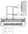
次に、プラズマ処理装置の概要を、図11の例を用いて説明する。本装置は、平行平板型のプラズマエッチング装置で、処理室1には電磁波放射のための略円板状のアンテナ3と、被処理体2を載置するための電極4が平行に対向して設置されている。アンテナ3にはプラズマ生成のための電磁波放射電源5Aが、整合器6Aを介して接続されている。
Next, an outline of the plasma processing apparatus will be described using the example of FIG. This apparatus is a parallel plate type plasma etching apparatus. In the processing chamber 1, a substantially disk-
アンテナ3の下部には、シャワープレート11が設置されている。処理ガスはガスボンベ20より供給され、ガス流量制御器13で所定の流量で流れ、シャワープレート11のガス孔を通して処理室1に導入される。また、プラズマ中のラジカル分布を制御するため、シャワープレート11の内側と外側でお互いに組成や流量の異なる処理ガスを導入できるようになっている。電極4にはRF電源5Cが整合器6Cを介して接続されており、被処理体2に入射するイオンを加速させ被処理体をエッチングする。
A
平行平板電極式RIE装置において、大口径ウェハに対して均一なエッチング処理を行うために、エッチング処理室内にステージ電極とガス供給電極を対向して設置し、ガス供給電極のガス供給面は第1のガス供給領域と第2のガス供給領域と第3のガス供給領域に分かれており、各々に対して第1のガス流量制御系と第2のガス流量制御系と第3のガス流量制御系を用いて個別に制御するように構成し、第1のガス供給領域と第2のガス供給領域と第3のガス供給領域より、エッチングガスの流量および電離電圧の異なるガスの流量比を最適化してガス供給を行なうことが、既に提案されている(例えば、特許文献1参照)。 In the parallel plate electrode type RIE apparatus, in order to perform a uniform etching process on a large-diameter wafer, a stage electrode and a gas supply electrode are installed facing each other in the etching process chamber, and the gas supply surface of the gas supply electrode is the first. The gas supply region, the second gas supply region, and the third gas supply region are divided into a first gas flow rate control system, a second gas flow rate control system, and a third gas flow rate control system, respectively. The gas flow rate of the etching gas and the gas flow rate having different ionization voltages are optimized from the first gas supply region, the second gas supply region, and the third gas supply region. It has already been proposed to supply gas (see, for example, Patent Document 1).
また、被処理体にプラズマエッチング処理を行う処理室と、処理ガスを供給するための第1のガス供給源と、第1の処理ガスとは別に設けられた第2のガス供給源と、処理ガスを前記処理室に導入する第1のガス導入口と、前記第1のガス導入口とは別に設けられた第2のガス導入口と、処理ガスの流量を調整する流量調節機と、処理ガスを複数に分割するガス分流器とを備え、ガス分流器と、第1または第2の少なくとも1つのガス導入口との間に、前記第2のガスを供給するようにしたプラズマエッチング装置により、処理ガスを2系統で供給することは、本願出願人らの出願になる特許出願(例えば、特許文献2参照)に提案されている。
ウェハなどの被処理体の面内において均一にエッチングするためには、被処理体の表面に入射するイオンの面内分布即ちプラズマ分布と、被処理体に堆積した堆積膜の厚さや組成を被処理体面内で均一にしなければならない。前述の従来のプラズマ処理装置は、被処理体面内で均一にプラズマ処理を行うため、プラズマ分布やラジカル分布を制御する手段を備えている。しかし、半導体装置の製造で重視される加工寸法には、加工深さとCD(Critical Dimension)があり、従来のプラズマ処理装置では加工深さの面内均一性とCD寸法の面内均一性をそれぞれ独立して制御できなかった。ここで、CD寸法とは被処理体の微細パターンにおける溝の幅や、線の幅や、孔の径などを指す。そのため、例えば加工深さの面内均一性を高めると、CD寸法の面内均一性が悪化することがあり、シャワープレートの内側と外側に流す処理ガスの流量と組成や、バイアス電力や、放電電力などを少しずつ調節して、加工深さの面内均一性とCD寸法の面内均一性を同時に満たす処理条件を見出さなければならない。 In order to perform uniform etching within the surface of a target object such as a wafer, the in-plane distribution of ions incident on the surface of the target object, that is, the plasma distribution, and the thickness and composition of the deposited film deposited on the target object are determined. It must be uniform within the surface of the treated body. The above-described conventional plasma processing apparatus includes means for controlling plasma distribution and radical distribution in order to perform plasma processing uniformly within the surface of the object to be processed. However, the processing dimensions important in the manufacture of semiconductor devices include processing depth and CD (Critical Dimension), and in the conventional plasma processing apparatus, in-plane uniformity of processing depth and in-plane uniformity of CD dimension are respectively provided. Could not be controlled independently. Here, the CD dimension refers to the width of a groove, the width of a line, the diameter of a hole, or the like in a fine pattern of an object to be processed. Therefore, for example, when the in-plane uniformity of the processing depth is increased, the in-plane uniformity of the CD dimension may deteriorate, and the flow rate and composition of the processing gas flowing inside and outside the shower plate, the bias power, and the discharge By adjusting power and the like little by little, it is necessary to find a processing condition that simultaneously satisfies the in-plane uniformity of the processing depth and the in-plane uniformity of the CD dimension.
CD寸法は、加工深さと比べても堆積膜の厚さと組成に大きく依存しているため、堆積膜の厚さや組成を適切に制御することで、加工深さの均一性を変えずにCD寸法の面内分布を均一にできれば望ましい。シャワープレートの内側のガス孔と外側のガス孔から導入するガスの組成や流量を制御する手法は、ラジカル分布制御の自由度が高いため、堆積膜の厚さや組成を適切に制御する手段として有望である。 Since the CD dimension greatly depends on the thickness and composition of the deposited film as compared with the processing depth, the CD dimension can be controlled without changing the uniformity of the processing depth by appropriately controlling the thickness and composition of the deposited film. It is desirable if the in-plane distribution can be made uniform. The method of controlling the composition and flow rate of the gas introduced from the gas holes inside and outside the shower plate is promising as a means to appropriately control the thickness and composition of the deposited film because of the high degree of freedom in radical distribution control. It is.
本発明は、上記課題を考慮し、被処理体の加工深さの均一性とCD寸法の均一性をそれぞれ独立して制御できる、すなわち加工深さの均一性を変えることなくCD寸法を制御できるようにガスの供給系を最適化したプラズマ処理装置の提供を目的としている。 In consideration of the above problems, the present invention can independently control the uniformity of the processing depth of the workpiece and the uniformity of the CD dimension, that is, the CD dimension can be controlled without changing the uniformity of the processing depth. An object of the present invention is to provide a plasma processing apparatus having an optimized gas supply system.
本発明のプラズマ処理装置は、処理室と、前記処理室に電磁波を放射するためのアンテナと、前記処理室内にガスを供給するためのシャワープレートと、前記シャワープレートに供給された前記ガスを分散させるガス分散板と、前記ガス分散板にガスを供給するガス供給手段と、前記処理室内を減圧する真空排気手段と、被処理体を載置する電極と、前記アンテナに高周波電力を供給する電磁波放射電源とを有するプラズマ処理装置であって、前記ガス供給手段は、複数のガス供給源から供給されたガス種毎に設けられたガス流量調節器を有し、前記ガス分散板は、内側の領域と外側の領域に分割され、OThe plasma processing apparatus of the present invention includes a processing chamber, an antenna for radiating electromagnetic waves to the processing chamber, a shower plate for supplying gas into the processing chamber, and the gas supplied to the shower plate is dispersed. A gas dispersion plate, a gas supply means for supplying gas to the gas dispersion plate, a vacuum exhaust means for reducing the pressure in the processing chamber, an electrode on which an object is placed, and an electromagnetic wave for supplying high-frequency power to the antenna A plasma processing apparatus having a radiation power source, wherein the gas supply means includes a gas flow rate controller provided for each gas type supplied from a plurality of gas supply sources, and the gas dispersion plate Divided into an area and an outer area, O
22
ガスおよびNGas and N
22
ガス以外の複数のガスからなる混合ガスである第1のガスの流量を所定のガス流量比に制御し、前記所定のガス流量比に制御されたガスを分配させる第一のガス分配手段と、OFirst gas distribution means for controlling the flow rate of the first gas, which is a mixed gas composed of a plurality of gases other than gas, to a predetermined gas flow rate ratio, and distributing the gas controlled to the predetermined gas flow rate ratio; O
22
ガスまたはNGas or N
22
ガス、あるいはOGas or O
22
ガスとNGas and N
22
ガスの混合ガスである第2のガスの流量を所定のガス流量比に制御し、前記所定のガス流量比に制御されたガスを分配させる第二のガス分配手段とを備え、前記第一のガス分配手段により分岐された一方の第1のガスが前記ガス分散板の内側の領域に、前記第一のガス分配手段により分岐された他方の第1のガスが前記ガス分散板の外側の領域にそれぞれ供給され、かつ、前記第二のガス分配手段により分岐された一方の第2のガスが前記ガス分散板の内側の領域に、前記第二のガス分配手段により分岐された他方の第2のガスが前記ガス分散板の外側の領域にそれぞれ供給されることによって、前記シャワープレートの内側領域と外側領域からそれぞれ供給される前記第2のガスの流量を前記第1のガスとは独立に制御できることを特徴とする。Second gas distribution means for controlling the flow rate of the second gas, which is a mixed gas of gas, to a predetermined gas flow rate ratio and distributing the gas controlled to the predetermined gas flow rate ratio, One first gas branched by the gas distribution means is in an area inside the gas dispersion plate, and the other first gas branched by the first gas distribution means is an area outside the gas distribution plate. And the second gas branched by the second gas distribution means is supplied to the inner region of the gas dispersion plate, and the other second gas branched by the second gas distribution means. Gas is supplied to the outer region of the gas dispersion plate, respectively, so that the flow rate of the second gas supplied from the inner region and the outer region of the shower plate can be made independent of the first gas. Features that can be controlled That.
さらに、本発明のプラズマ処理装置においては、前記処理室に磁場を生成させる磁場生成手段を有することを特徴とする。Furthermore, the plasma processing apparatus of the present invention is characterized by having magnetic field generation means for generating a magnetic field in the processing chamber.
さらに、本発明のプラズマ処理装置は、前記アンテナは内側領域と外側領域に分割され、前記電磁波放射電源は、分配器により前記アンテナの内側領域と前記アンテナの外側領域にそれぞれ高周波電力を供給することを特徴とする。Further, in the plasma processing apparatus of the present invention, the antenna is divided into an inner region and an outer region, and the electromagnetic wave radiation power source supplies high frequency power to the inner region of the antenna and the outer region of the antenna by a distributor, respectively. It is characterized by.
またさらに、本発明のプラズマ処理装置は、前記載置電極の内側領域に高周波電力を供給する第一の高周波電源と、前記載置電極の外側領域に高周波電力を供給する第二の高周波電源とを有することを特徴とする。Furthermore, the plasma processing apparatus of the present invention includes a first high-frequency power source that supplies high-frequency power to the inner region of the placement electrode, and a second high-frequency power source that supplies high-frequency power to the outer region of the placement electrode. It is characterized by having.
さらに、本発明のプラズマ処理装置は、前記第一のガス分配手段は、ガス分配器を有することを特徴とする。Furthermore, the plasma processing apparatus of the present invention is characterized in that the first gas distribution means has a gas distributor.
またさらに、本発明のプラズマ処理装置は、前記第一及び第二のガス分配手段は、ガス分配器を有することを特徴とする。Furthermore, the plasma processing apparatus of the present invention is characterized in that the first and second gas distribution means have gas distributors.
またさらに、本発明のプラズマ処理装置は、前記第一のガス分配手段は、ガス分配器を有し、前記第二のガス分配手段は、前記OStill further, in the plasma processing apparatus of the present invention, the first gas distribution unit includes a gas distributor, and the second gas distribution unit includes the O
22
ガスまたはNGas or N
22
ガス、あるいはOGas or O
22
ガス及びNGas and N
22
ガスがそれぞれ複数のガス流量調整器で供給されることにより、前記OThe gas is supplied by a plurality of gas flow regulators, so that the O
22
ガスまたはNGas or N
22
ガス、あるいはOGas or O
22
ガス及びNGas and N
22
ガスを分配することを特徴とする。It is characterized by distributing gas.
またさらに、本発明のプラズマ処理装置は、前記ガス分散板を複数の領域に仕切るためのO−リングを設け、前記O−リングにより前記ガス分散板が浮き上がらないように、ガス分散板をアンテナにネジでとめたことを特徴とする。Furthermore, the plasma processing apparatus of the present invention is provided with an O-ring for partitioning the gas dispersion plate into a plurality of regions, and the gas dispersion plate is used as an antenna so that the O-ring does not lift the gas dispersion plate. It is characterized by being fastened with screws.
またさらに、本発明のプラズマ処理装置は、前記ガス分散板には、第1のガス噴出口と、第2のガス噴出口とを設け、前記アンテナには、第1のガス流路と、第2のガス流路を設置し、前記ガス分散板にガスを供給するための前記第1のガス流路の出口、あるいは前記第2のガス流路の出口は、前記アンテナの略中心を中心点として略円周上に複数個設置されていることを特徴とする。Furthermore, in the plasma processing apparatus of the present invention, the gas dispersion plate is provided with a first gas outlet and a second gas outlet, and the antenna has a first gas passage, The outlet of the first gas passage or the outlet of the second gas passage for supplying gas to the gas dispersion plate is centered on the approximate center of the antenna. It is characterized in that a plurality are installed on a substantially circumference.
またさらに、本発明のプラズマ処理装置は、前記シャワープレートに開けられたガス噴出口は、前記シャワープレートの略中心から同心円状に配置されていることを特徴とする。Furthermore, the plasma processing apparatus of the present invention is characterized in that the gas jets opened in the shower plate are arranged concentrically from the approximate center of the shower plate.
このように、本発明では、処理室と、処理室に処理ガスを供給する手段と、処理室を減圧する真空排気手段と、被処理体を載置する電極と、電磁波放射電源とを有するプラズマ処理装置において、OThus, in the present invention, a plasma having a processing chamber, means for supplying a processing gas to the processing chamber, evacuation means for depressurizing the processing chamber, an electrode for mounting the object to be processed, and an electromagnetic wave radiation power source. In processing equipment, O
22
あるいはNOr N
22
の組成比あるいは流量比が異なる少なくとも2種類の処理ガスを、互いに異なるガス導入口から導入することで、被処理体の面内における加工深さを均一に保ったまま、被処理体面内でCD寸法を均一にできるようにする。By introducing at least two types of processing gases having different composition ratios or flow rate ratios from different gas inlets, the processing depth in the surface of the object to be processed is kept uniform while maintaining the processing depth in the surface of the object to be processed. Make the dimensions uniform.
さらに、本発明では、OFurthermore, in the present invention, O
22
とNAnd N
22
以外の処理ガスを第1の処理ガスとして複数に分配し、分配した後の第1のガスに第2のガスとしてOA processing gas other than the above is distributed as a first processing gas into a plurality of gases, and the first gas after the distribution is supplied with O as a second gas.
22
とNAnd N
22
を添加することで、互いにOTo each other,
22
あるいはNOr N
22
の組成や流量が異なる処理ガスを、互いに異なるガス導入口から処理室内に導入できるようにする。このとき、複数に分配した後の第1のガスに添加するOThe processing gases having different compositions and flow rates can be introduced into the processing chamber from different gas inlets. At this time, O added to the first gas after being distributed in plural.
22
あるいはNOr N
22
の添加量に関わらず、第1の処理ガスが所定の流量比に分配できるように、第1のガスを複数に分配するためのガス分配器を用いる。A gas distributor for distributing the first gas into a plurality of parts is used so that the first process gas can be distributed at a predetermined flow rate ratio regardless of the amount of the added gas.
さらに、本発明では、複数に分配した第1のガスにO 2 あるいはN 2 を所定の流量比で添加するため、O 2 あるいはN 2 を、所定の流量比で分配するためのガス分配器を備えることとする。
Furthermore, in the present invention, a gas distributor for distributing O 2 or N 2 at a predetermined flow rate ratio is added in order to add O 2 or N 2 to the first gas distributed at a predetermined flow rate ratio. I will prepare.
さらに、本発明では、ガス分配器が正常に機能しているかをモニタするため、処理室内に設けられた第1のガス噴出口と前記ガス分配器との間、および、処理室内に設けられた第2のガス噴出口と前記ガス分配器の間に、ガス流量計を備えたことを特徴とする。
Furthermore, in the present invention, in order to monitor whether the gas distributor is functioning normally , the gas distributor is provided between the first gas outlet provided in the processing chamber and the gas distributor, and in the processing chamber. A gas flow meter is provided between the second gas outlet and the gas distributor.
さらに、本発明では、前記ガス分配器が正常に動作するかをチェックできるようにするため、処理室内に設けられた第1のガス噴出口と前記ガス分配器の間、および、処理室内に設けられた第2のガス噴出口と前記ガス分配器との間に、処理室内を経由せずに処理ガスを排気するためのガスラインを接続したことを特徴とする。 Further, in the present invention, in order to check whether or not the gas distributor operates normally, it is provided between the first gas outlet provided in the processing chamber and the gas distributor, and in the processing chamber. A gas line for exhausting the processing gas without passing through the processing chamber is connected between the second gas ejection port formed and the gas distributor .
さらに、本発明では、ガス分散板において、第2のガスを分散させる領域の形状をドーナツ状とし、ドーナツ状の領域にガスを均等に分散させるため、第2の処理ガスを分散板に噴出するためのガス噴出口を、略円周上に複数個配置したことを特徴とする。 Furthermore, in the present invention, in the gas dispersion plate, the shape of the region in which the second gas is dispersed is made donut-shaped, and the second processing gas is jetted onto the dispersion plate in order to uniformly disperse the gas in the donut-shaped region. For this purpose, a plurality of gas outlets are arranged substantially on the circumference.
以上説明したように、本発明では、O2あるいはN2の組成比あるいは流量比が異なる少なくとも2種類の処理ガスを、互いに異なるガス導入口から所定の流量および組成で処理室内に導入することによって、加工深さの面内均一性とは独立に、CD寸法を被処理体面内で均一にすることができる。これにより、被処理体面内における加工深さとCD寸法の両方の均一性を高めることができる。 As described above, in the present invention, at least two kinds of processing gases having different O 2 or N 2 composition ratios or flow rate ratios are introduced into the processing chamber at different flow rates and compositions from different gas inlets. Independent of the in-plane uniformity of the processing depth, the CD dimension can be made uniform in the surface of the object to be processed. Thereby, the uniformity of both the processing depth and CD dimension in the to-be-processed object surface can be improved.
以下、本発明の第1の実施例について図面を参照して説明する。図1は、平行平板型のECRプラズマ処理装置において、本発明を適用した第1の実施例を示している。処理室1には、電磁波放射のための略円板状のアンテナ3と被処理体2を載置するための電極4が平行に対向して設置されている。アンテナ3には、プラズマ生成のための電磁波放射電源5Aが、整合器6Aを介して接続されている。該電磁波放射電源5Aの周波数は、例えば100〜450MHzとする。処理室1の外側には、コイル8とヨーク9が設置されており磁場を生成する。本装置は、磁場と電場の相互作用によりプラズマを効率よく生成するとともに、磁場分布を調節することでプラズマの生成位置やプラズマの輸送を制御できることが特徴である。
A first embodiment of the present invention will be described below with reference to the drawings. FIG. 1 shows a first embodiment to which the present invention is applied in a parallel plate type ECR plasma processing apparatus. In the processing chamber 1, a substantially disc-shaped
アンテナ3の下部には、分散板10を介してシャワープレート11が設置されている。該シャワープレート11の材料は、Siである。アンテナ3には、電磁波放射電源5Aの他に、RF電源5Bが整合器6Bを介して接続されており、プラズマ分布やFなどのラジカル分布を制御することができる。該RF電源5Bの周波数は、数百kHz〜十数MHzとする。
A
本装置では、アンテナの上部を大気とするため、アンテナ3や石英部品28をO−リング21によってシールしている。
In this apparatus, the
電極4には、被処理体2に入射するイオンのフラックスやイオンの入射エネルギーを制御するため、RF電源5Cが整合器6Cを介して接続されている。該RF電源は、RF電源5Bと同じ周波数とし、位相制御機7によりRF電源6BとRF電源6Cで発生するRF電力を逆位相にすることで、プラズマの閉じ込めを向上させることができる。電極4は、上下に可動でき、アンテナ3と電極4の距離によって、プラズマの分布とラジカル分布を制御することができる。
An
電極4の内部には、被処理体2の温度を制御するため冷媒が流れるようになっている(図示せず)。さらに、被処理体2の裏面と電極の間に被処理体を冷却するためのヘリウムを流すため、電極4の表面にはヘリウムを流すための溝が作られている。また、被処理体の外周と内側において被処理体の温度を独立に制御するため、電極の内側と外周でヘリウムの流路が仕切られている。そして、電極の内側に流すヘリウムの導入路16−1と、電極の外周に流すヘリウムの導入路16−2から、お互いに異なる流量のヘリウムを電極の内側と外周に流すことができるようになっている。
A coolant flows through the
被処理体2を電極4に静電吸着によって固定させるため、電極4にはダイポール電源(図示せず)が接続されている。また、処理室はアース電位にしてある。
In order to fix the
処理ガスは、電磁波放射アンテナ3とガス分散板10とシャワープレート11を通して処理室1に供給される。シャワープレート11には複数個のガス孔が開けてあり、該ガス孔の配置は、例えば直径300mmの範囲に10mm間隔で略同心円状に開けてある。
The processing gas is supplied to the processing chamber 1 through the electromagnetic
ガス分散板10は、プラズマ中のラジカル分布を制御するため、略リング状の仕切り12で仕切られており、該略リング状の仕切り12の内側に位置するシャワープレート11のガス孔(以後「内側のガス孔」と呼ぶ)と該略リング状の仕切り12の外側に位置するシャワープレート11のガス孔(以後「外側のガス孔」と呼ぶ)から、お互いに組成や流量の異なる処理ガスを処理室1に導入できるようにしてある。該略リング状の仕切り12には、例えばO−リングを用い、該リング状の仕切りの内径は、50mmから250mm程度とする。
The
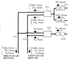
処理室1に導入する処理ガスは、例えばAr、CHF3、CH2F2、CH4、C4F6、C4F8、C5F8、CO、O2、N2とする。該処理ガスのうち、Arと、CH4と、C4F6と、C4F8と、C5F8と、CHF3と、CH2F2と、COは、それぞれガス流量調節器13−1〜13−8において所定の流量で流れ、第1のガス分配器14−1に到達する。該第1のガス分配器14−1に到達したガスを第1のガスとする。該第1のガスは、該第1のガス分配器14−1において、内側のガス孔から導入する第1のガスと外側のガス孔から導入する第1のガスに所定の流量比で分配される。
The processing gas introduced into the processing chamber 1 is, for example, Ar, CHF 3 , CH 2 F 2 , CH 4 , C 4 F 6 , C 4 F 8 , C 5 F 8 , CO, O 2 , and N 2 . Among the processing gases, Ar, CH 4 , C 4 F 6 , C 4 F 8 , C 5 F 8 , CHF 3 , CH 2 F 2 , and CO are
O2とN2は、それぞれガス流量調節器13−9、13−10において所定の流量で流れ、第2のガス分配器14−2に到達する。該第2のガス分配器14−2に到達したガスを第2のガスとする。第2のガスは、第2のガス分配器14−2によって所定の流量比で分配され、一方は、ガスの合流点15−1で内側のガス孔から導入する第1のガスに混合され、他方は、ガスの合流点15−2において外側のガス孔から導入する第1のガスに混合される。 O 2 and N 2 flow at a predetermined flow rate in the gas flow rate controllers 13-9 and 13-10, respectively, and reach the second gas distributor 14-2. The gas that has reached the second gas distributor 14-2 is defined as a second gas. The second gas is distributed at a predetermined flow rate ratio by the second gas distributor 14-2, and one is mixed with the first gas introduced from the inner gas hole at the gas confluence 15-1; The other is mixed with the first gas introduced from the outer gas hole at the gas confluence 15-2.
処理室1には、該処理室1を減圧するため、ターボ分子ポンプ25がゲートバルブ24を介して接続されており、処理ガスを流した状態で、処理室1を所定の圧力に維持することができる。該ターボ分子ポンプ25の排気側には、ドライポンプ26が接続されている。
A turbo
次に、加工深さとCD寸法をウェハ面内で均一にする手順について、SiOC膜の深孔エッチングを例に述べる。第1のガスにはCF4とCHF3を用い、ガス流量調節器13−2とガス流量調節器13−6においてCF4とCHF3の流量をそれぞれ20ccmとした。第2のガスにはN2を用い、ガス流量調節器13−10において流量を100ccmとした。 Next, a procedure for making the processing depth and the CD dimension uniform within the wafer surface will be described by taking deep hole etching of the SiOC film as an example. CF 4 and CHF 3 were used as the first gas, and the flow rates of CF 4 and CHF 3 were set to 20 ccm in the gas flow rate regulator 13-2 and the gas flow rate regulator 13-6, respectively. N 2 was used as the second gas, and the flow rate was set to 100 ccm in the gas flow rate regulator 13-10.
まず、内側のガス孔から導入する処理ガスと外側のガス孔から導入する処理ガスをお互いに同じ組成にし、磁場によるプラズマ分布制御を行わないでエッチングを行った。ガス供給系におけるガスの流れを図3に示す。第1のガス分配器14−1では、CF4とCHF3の混合ガス40ccmを、20ccmずつ均等に分配し、第2のガス分配器14−2では、N2を50ccmずつ均等に分配している。この場合の加工深さおよび孔底のCD寸法のウェハ面内分布を図2(A)に示す。エッチング速度がウェハ中心部で高くウェハ外周部で低くなり、ウェハ中心ではウェハ外周に比べて孔が深く、孔底のCD寸法は小さくなっている。 First, the processing gas introduced from the inner gas hole and the processing gas introduced from the outer gas hole have the same composition, and etching was performed without performing plasma distribution control by a magnetic field. FIG. 3 shows the gas flow in the gas supply system. In the first gas distributor 14-1, a mixed gas of CF 4 and CHF 3 of 40 ccm is evenly distributed by 20 ccm, and in the second gas distributor 14-2, N 2 is uniformly distributed by 50 ccm. Yes. FIG. 2A shows the in-wafer distribution of the processing depth and the hole bottom CD dimension in this case. The etching rate is high at the center of the wafer and low at the periphery of the wafer, the hole is deeper at the center of the wafer than at the periphery of the wafer, and the CD dimension at the bottom of the hole is small.
次に、ウェハ面内において加工深さを均一にするため、磁場によりプラズマ分布制御を行った。このときの加工深さおよび孔底のCD寸法のウェハ面内分布を図2(B)に示す。磁場を加えることにより、エッチング速度の面内分布を均一にすることができ、加工深さの面内分布を均一にできることが分かる。一方で、ウェハ中心で孔底のCD寸法は小さいままであり、これはウェハ中心部で堆積膜が過剰に厚いか、あるいはエッチング阻害物の堆積量が多いと推測される。 Next, in order to make the processing depth uniform within the wafer surface, plasma distribution control was performed using a magnetic field. FIG. 2B shows the in-wafer distribution of the processing depth and hole bottom CD dimension at this time. It can be seen that by applying a magnetic field, the in-plane distribution of the etching rate can be made uniform, and the in-plane distribution of the processing depth can be made uniform. On the other hand, the CD size of the hole bottom remains small at the center of the wafer, which is presumed that the deposited film is excessively thick at the center of the wafer or the amount of deposition of the etching inhibitor is large.
次に、図4に示すように、磁場によりプラズマ分布制御を行いながら、CF4とCHF3については内側のガス孔と外側のガス孔からそれぞれ10ccmずつ均等に処理室に導入し、堆積膜除去に寄与するN2は内側のガス孔と外側のガス孔からそれぞれ80ccmと20ccmの流量で導入するようにした。このとき、第1のガス分配器14−1ではCF4とCHF3の混合ガス40ccmを、20ccmずつ均等に分配し、第2のガス分配器14−2においてはN2を8:2の流量比で分配している。即ち、第1のガス分配器14−1と第2のガス分配器14−2によって、内側のガス孔と外側のガス孔から処理室内に供給するCF4およびCHF3の流量を変えずに、内側のガス孔から供給するとN2と外側のガス孔から処理室内に供給するN2の流量比を制御している。この場合の加工深さおよび孔底のCD寸法のウェハ面内分布を図2(C)に示す。図2(B)との比較からわかるように、加工深さの面内均一性を変えずにウェハ面内における孔底のCD寸法を均一にできることが分かる。 Next, as shown in FIG. 4, while performing plasma distribution control by a magnetic field, CF 4 and CHF 3 are introduced uniformly into the processing chamber by 10 ccm from the inner gas hole and the outer gas hole, respectively, and the deposited film is removed. N 2 which contributes to the gas was introduced at a flow rate of 80 ccm and 20 ccm from the inner gas hole and the outer gas hole, respectively. At this time, the first gas distributor 14-1 uniformly distributes 40 ccm of the mixed gas of CF 4 and CHF 3 by 20 ccm, and the second gas distributor 14-2 supplies N 2 at a flow rate of 8: 2. The ratio is distributed. That is, the first gas distributor 14-1 and the second gas distributor 14-2 do not change the flow rates of CF 4 and CHF 3 supplied from the inner gas hole and the outer gas hole into the processing chamber, and it controls the is supplied from the inside of the gas holes N 2 and outer flow ratio of supplied N 2 from gas holes into the processing chamber. FIG. 2C shows the in-wafer distribution of the processing depth and hole bottom CD dimension in this case. As can be seen from the comparison with FIG. 2B, it can be seen that the CD dimension of the hole bottom in the wafer surface can be made uniform without changing the in-plane uniformity of the processing depth.
上記の説明では、第1のガス分配器14−1では第1のガスを均等に分配しているが、図2(B)の状態でさらに第1のガス分配器14−1のガス分配比を調節し、内側のガス孔から供給する第1のガスと外側のガス孔から供給する第1のガスの流量比を制御することで、加工深さの均一性を高めることができる。ただし、第1のガス分配器14−1の分配比を調整して加工深さの均一性を高めると、CD寸法の面内均一性が変化することがあるため、第1のガス分配器14−1における第1のガスの分配比は、CD寸法の面内分布を均一にする前に調節するのが望ましい。 In the above description, the first gas distributor 14-1 distributes the first gas evenly. However, the gas distribution ratio of the first gas distributor 14-1 in the state of FIG. By adjusting the flow rate and controlling the flow ratio of the first gas supplied from the inner gas hole and the first gas supplied from the outer gas hole, the uniformity of the processing depth can be improved. However, if the uniformity of the processing depth is increased by adjusting the distribution ratio of the first gas distributor 14-1, the in-plane uniformity of the CD dimension may change. Therefore, the first gas distributor 14 It is desirable to adjust the distribution ratio of the first gas at −1 before making the in-plane distribution of the CD dimension uniform.
以上、SiOCの加工において、加工深さは磁場により均一にし、孔底のCD寸法は内側のガス孔と外側のガス孔から導入するN2の流量比を調節することで均一にできることを示した。SiO2やSiOFのエッチングにおいては、例えばArとC4F8などのCF系ガスとO2を用いるが、この場合は第2のガス分配器14−2において、O2の分配比を調節することで、ウェハ面内での加工深さを均一に保ったまま、孔底などのCD寸法をウェハ面内で均一にすることができる。 As described above, in the processing of SiOC, it has been shown that the processing depth can be made uniform by a magnetic field, and the CD size of the hole bottom can be made uniform by adjusting the flow rate ratio of N 2 introduced from the inner gas hole and the outer gas hole. . In the etching of SiO 2 or SiOF, for example, CF gas such as Ar and C 4 F 8 and O 2 are used. In this case, the distribution ratio of O 2 is adjusted in the second gas distributor 14-2. Thus, the CD dimension such as the hole bottom can be made uniform in the wafer surface while the processing depth in the wafer surface is kept uniform.
次に、ガス分配器の動作の確認方法について述べる。第1のガス分配器14−1と処理室1との間にガス流量計22−1、22−2が設置され、第2のガス分配器14−2と処理室1との間にガス流量計22−3、22−4が設置されている。例えば、第1のガスを流した状態で、ガス流量計22−1,22−2の流量比と、第1のガス分配器14−1で設定したガス分配比を比較することで、第1のガス分配器14−1が正常に動作しているかをチェックすることができる。 Next, a method for confirming the operation of the gas distributor will be described. Gas flow meters 22-1 and 22-2 are installed between the first gas distributor 14-1 and the processing chamber 1, and the gas flow rate between the second gas distributor 14-2 and the processing chamber 1 is set. A total of 22-3 and 22-4 are installed. For example, by comparing the flow rate ratio of the gas flow meters 22-1 and 22-2 with the gas distribution ratio set by the first gas distributor 14-1 in a state where the first gas is flowed, It is possible to check whether the gas distributor 14-1 is operating normally.
また、第1のガスを流さないで、第2のガスを流し、ガス流量計22−3,22−4の流量比と第2のガス分配器14−2で設定したガス分配比を比較することで、第2のガス分配器14−2が正常に動作しているかをチェックすることができる。 Further, the second gas is flowed without flowing the first gas, and the flow ratio between the gas flow meters 22-3 and 22-4 is compared with the gas distribution ratio set by the second gas distributor 14-2. Thus, it is possible to check whether the second gas distributor 14-2 is operating normally.
さらに、第1のガス分配器14−1および第2のガス分配器14−2の下流で処理室1の上流側にバルブ23−1,23−2を設け、この弁の上流側でかつガス流量計22−3,22−4の下流側で、バルブ23−3,23−4を設けたガス配管を分岐させ、処理ガスを処理室内1を経由せずに、例えば、ドライポンプ26で排気できるようにすることで、ガス分配器の動作をチェックできるようにしてある。第1のガス分配器14−1を例に、以下に、その動作チェック手順を説明する。
Furthermore, valves 23-1 and 23-2 are provided on the upstream side of the processing chamber 1 downstream of the first gas distributor 14-1 and the second gas distributor 14-2. The gas pipe provided with the valves 23-3 and 23-4 is branched downstream of the flow meters 22-3 and 22-4, and the processing gas is exhausted by the
まず、バルブ23−1とバルブ23−4を開け、バルブ23−2とバルブ23−3を閉じ、内側のガス孔から供給する処理ガスは、そのまま処理室1に導入され、通常は外側のガス孔から導入する処理ガスは、処理室1内を経由せずにドライポンプ26で排気されるようにしておく。そしてゲートバルブ24とバルブ23−5を閉じ、例えば、Arガス500ccmを流す。第1のガス分配器14−1におけるガス配分比は、例えばa:bに設定する。処理室1の容積と圧力の上昇速度から内側のガス孔から処理室1に導入されたArガスの流量を計算でき、求めた値をAとする。
First, the valve 23-1 and the valve 23-4 are opened, the valve 23-2 and the valve 23-3 are closed, and the processing gas supplied from the inner gas hole is introduced into the processing chamber 1 as it is, and usually the outer gas. The processing gas introduced from the hole is exhausted by the
次に、バルブ23−2とバルブ23−3をあけ、バルブ23−1と、バルブ23−4を閉じ、通常は内側のガス孔から供給する処理ガスは、処理室1に導入しないでドライポンプ26で排気し、外側のガス孔から導入する処理ガスはそのまま処理室1に導入されるようにしておく。そして、Arガス500ccmを流し、第2のガス分配器14−1の流量比をa:bのままにしておく。このときの処理室1の容積と圧力上昇速度からArガスの流量を計算し、求めた流量値をBとする。そして、A:Bとa:bの比を比較することで、第1のガス分配器14−1が正常に動作しているかを確認できる。 Next, the valve 23-2 and the valve 23-3 are opened, the valve 23-1 and the valve 23-4 are closed, and the processing gas normally supplied from the inner gas hole is not introduced into the processing chamber 1 and is dry pumped. The processing gas exhausted at 26 and introduced from the outer gas hole is introduced into the processing chamber 1 as it is. And Ar gas 500ccm is flowed and the flow rate ratio of the 2nd gas distributor 14-1 is left as a: b. The flow rate of Ar gas is calculated from the volume of the processing chamber 1 and the pressure increase rate at this time, and the obtained flow rate value is B. Then, by comparing the ratio of A: B and a: b, it can be confirmed whether the first gas distributor 14-1 is operating normally.
以上、第1の実施例を説明したが、第1の実施例のようなガスの供給制御は、ガス分配器を用いなくても可能である。そこで、次に、第2の実施例を、図5を用いて説明する。図5において、図1と重複する部分の説明は省略する。本実施例では、1つの処理ガス毎に、内側のガス孔からの供給量を調節するためガス流量調節器13−11〜13−20と、外側のガス孔からの供給量を調節するためのガス流量調節器13−1〜13−10を備えている。図1との比較からわかるように、ガス流量調節器13の必要台数がガス分配器14を用いた場合と比べて多くなるが、図1と同様なガス供給制御が可能である。
Although the first embodiment has been described above, the gas supply control as in the first embodiment is possible without using a gas distributor. Therefore, the second embodiment will be described with reference to FIG. In FIG. 5, the description of the same part as in FIG. 1 is omitted. In this embodiment, for each processing gas, the gas flow rate regulators 13-11 to 13-20 for adjusting the supply amount from the inner gas hole and the supply amount from the outer gas hole are adjusted. Gas flow regulators 13-1 to 13-10 are provided. As can be seen from the comparison with FIG. 1, the required number of gas
上記の第1および第2の実施例は、磁場によるプラズマ分布制御の自由度の大きい平行平板型のECRプラズマ処理装置に本発明を適用した場合について示したものであるが、本発明は、磁場以外の手段によってプラズマ分布の均一性を制御する方式のプラズマ処理装置にも広く適応できる。 The first and second embodiments described above show the case where the present invention is applied to a parallel plate type ECR plasma processing apparatus with a high degree of freedom of plasma distribution control by a magnetic field. The present invention can be widely applied to plasma processing apparatuses that control the uniformity of plasma distribution by means other than the above.
その例として、次に、本発明の第3の実施例について説明する。図6は、CCP(Capacitively Coupled Plasma)方式のプラズマ処理装置に本発明を適用した場合について示している。本装置は、例えば10MHz〜200MHzの周波数の電磁波を電磁波放射アンテナから放出させ、電極間に発生する高周波電界によりプラズマを生成している。電磁波放射アンテナは例えば内側のアンテナ3−1と外側のアンテナ3−2の2つに分割してあり、高周波電力の分配器17によって内側のアンテナ3−1と外側のアンテナ3−2から放射する高周波電力の比を変えることでプラズマ分布制御の自由度を高めている。処理室1には被処理体2を載置する電極4が設置され、被処理体2に入射するイオンのフラックスやイオンの入射エネルギーを制御するため高周波電源5Cが整合器6Cを介して電極4に接続されている。図6に示した第3の実施例では、ガス流量調節器とガス分配器14−1,14−2の組み合わせは第1の実施例と同じとなっているが、第2の実施例と同じようなガス供給系にしてもよい。
As an example, a third embodiment of the present invention will be described next. FIG. 6 shows a case where the present invention is applied to a CCP (Capacitively Coupled Plasma) type plasma processing apparatus. In this apparatus, for example, an electromagnetic wave having a frequency of 10 MHz to 200 MHz is emitted from an electromagnetic wave radiation antenna, and plasma is generated by a high frequency electric field generated between the electrodes. The electromagnetic wave radiation antenna is divided into, for example, an inner antenna 3-1 and an outer antenna 3-2, and is radiated from the inner antenna 3-1 and the outer antenna 3-2 by a high
図7にガス分散板10を、内側のガス孔から処理室内に導入する処理ガスを分散させるための領域と、外周のガス孔から処理室内に導入する処理ガスを分散させるための領域の2つに分割している部分を拡大して示す。第3の実施例では、2枚のガス分散板10−1、10−2を積み重ねて用いて、処理ガスを分散させている。ガス分配板10−1,10−2は、リング状仕切り(例えばO−リング)12−1,12−2を用いてそれぞれ2つの領域に仕切られている。またO−リングの厚みにより、ガス分配板10−1、10−2が撓まないようにするため、例えば、アルミ製のスペーサ33を介してねじ32によって、ガス分散板10−1,10−2をアンテナ3にねじ止めしている。また、ガス分散板10−1、10−2とアンテナ3は、内側アンテナ3−1と外側アンテナ3−2でお互いにパワーの異なる高周波電力を印加できるようにするため、絶縁物31によって分離されている。
In FIG. 7, the
次に、図6と処理室の上方から見たときのアンテナ3の形状を示す図8を用いて、アンテナ3へのガスの供給と高周波電力の入力について説明する。内側のアンテナ3−1に供給する高周波電力は、内側のアンテナ3−1の略中央に配置された電力接続部34−1を介して印加される。外側のアンテナ3−2に供給する高周波電力は、外側のアンテナ3−2の略円周上に配置された電力接続部34−2を介して供給される。
Next, gas supply to the
内側のガス孔から処理室内に導入する処理ガスは、電力接続部34−1を避けて設けられたガス導入口35−1から内側のアンテナ3−1の内部に導入し、アンテナ内に設けられたガスの流路27−1を通ってアンテナの略中央部に設けたガス噴出口36−1からガス分散板10―1上に噴出される。外側のガス孔から処理室内に導入する処理ガスは、外側のアンテナ3−2の上部から、アンテナのガス導入口35−2から導入され、外側のアンテナ3−2内部に設けられたガスの流路27−2を通ってガス噴出口36−2からガス分散板10−1の上部外周側に噴出される。外側のガス孔から処理室内に導入される処理ガスが、シャワープレートの外側のガス孔から均等に処理室内に導入されるようにするため、外側のガス孔から処理室内に導入する処理ガスをアンテナ内部に導入するためのガス導入口35−2は略同心円状に複数個配置されている。そして、外側のガス孔から処理室内に導入する処理ガスを、ガス分散板10−1の外側領域で均等に分散させるため、外側のガス孔から処理室内に導入する処理ガスをガス分散板に噴出させるためのガス噴出口36−2は外側のアンテナ3−2に略円周上に複数個配置されているものとする。 The processing gas introduced into the processing chamber from the inner gas hole is introduced into the inner antenna 3-1 through the gas inlet 35-1 provided avoiding the power connection portion 34-1, and provided in the antenna. Then, the gas is ejected onto the gas dispersion plate 10-1 from the gas ejection port 36-1 provided in the substantially central portion of the antenna through the gas flow path 27-1. The processing gas introduced into the processing chamber from the outer gas hole is introduced from the upper part of the outer antenna 3-2 through the gas inlet 35-2 of the antenna, and the gas flow provided inside the outer antenna 3-2. The gas is ejected from the gas ejection port 36-2 to the upper outer peripheral side of the gas dispersion plate 10-1 through the path 27-2. The processing gas introduced from the outer gas hole into the processing chamber is introduced into the processing chamber through the outer gas hole so that the processing gas introduced into the processing chamber from the outer gas hole of the shower plate is evenly introduced into the processing chamber. A plurality of gas introduction ports 35-2 for introduction into the inside are arranged substantially concentrically. And in order to disperse | distribute the process gas introduce | transduced into a process chamber from an outer gas hole equally in the outer area | region of the gas dispersion | distribution board 10-1, the process gas introduced into a process chamber is blown out to a gas dispersion | distribution board from an outer gas hole. It is assumed that a plurality of gas outlets 36-2 are arranged on the outer antenna 3-2 substantially on the circumference.
本装置において、被処理体面内で均一にエッチングするためには、最初に、例えば、内側アンテナ3−1と外側アンテナ3−2から放射される高周波電力のパワー比を調節するなどにより、加工深さを被処理体面内で均一にする。そして、内側のガス孔と外周のガス孔から処理室内に導入するO2あるいはN2ガスの流量比を調節すれば、被処理体面内において加工深さを均一に保ったまま、被処理体面内におけるCD寸法を均一にすることができる。 In this apparatus, in order to etch uniformly within the surface of the object to be processed, first, for example, by adjusting the power ratio of the high frequency power radiated from the inner antenna 3-1 and the outer antenna 3-2, the processing depth is adjusted. The thickness is made uniform in the surface of the object to be processed. If the flow rate ratio of O 2 or N 2 gas introduced into the processing chamber from the inner gas hole and the outer gas hole is adjusted, the processing depth is maintained within the processing target surface while maintaining the processing depth uniform in the processing target surface. The CD dimension can be made uniform.
次に、第4の実施例を、図9を用いて説明する。本実施例の装置では、周波数の異なる2つの高周波電源5Aと高周波電源5Cがそれぞれ整合器6Aと整合器6Cを介して電極4に接続されている。本装置は、高周波電源5Aと高周波電源5Cから出力された高周波電力によってプラズマを生成すると共に、高周波電源5Aの出力電力と高周波電源5Cの出力電力のバランスによってプラズマの分布を制御することができる。
Next, a fourth embodiment will be described with reference to FIG. In the apparatus of the present embodiment, two high
本装置において、被処理体面内で均一にエッチングを行うためには、例えば高周波電源5Aの出力電力と高周波電源5Cの出力電力のバランスを調節することによりプラズマ分布制御を行い、加工深さを処理体面内で均一にする。そして、天板のガス噴出口36-1,36-2を経由してシャワープレート11の内側のガス孔と外側のガス孔から処理室1に供給するO2あるいはN2の流量比を調節することにより、加工深さを被処理体面内で均一に保ったまま、CD寸法を被処理体面内で均一にすることができる。
In this apparatus, in order to perform etching uniformly within the surface of the object to be processed, for example, the plasma distribution control is performed by adjusting the balance between the output power of the high
以上、各種プラズマ源について本発明の実施例を説明したが、本発明はこれらのプラズマ源への適用に限定されることはなく、他のプラズマ処理装置などに広く適用することができる。 As mentioned above, although the Example of this invention was described about various plasma sources, this invention is not limited to application to these plasma sources, It can apply widely to other plasma processing apparatuses.
1:処理室、2:被処理体、3:電磁波放射アンテナ、4:被処理体載置電極、5A:電磁波放射電源、5B:電磁波放射アンテナに接続されたRF電源、5C:被処理体載置電極に接続されたRF電源、6A:電磁波放射電源のための整合器、6B:電磁波放射アンテナに接続されたRF電源のための整合器、6C:被処理体載置電極に接続されたRF電源のための整合器、7:位相制御器、8:磁場コイル、9:ヨーク、10:ガス分散板、11:シャワープレート、12:ガス分散板の仕切り、13:ガス流量調節器、14:ガス分配器、15:ガス配管の合流点、16…冷却用ヘリウムの導入路、17:高周波電力分配器、51:SiOC、52:レジスト、53:堆積膜、20:ガスボンベ、21:O−リング、22:流量計、23:バルブ、24:ゲートバルブ、25:ターボ分子ポンプ、26:ドライポンプ、27:ガス流路、28:石英部品、31:絶縁物、32:ねじ、33:スペーサ、34:電力接続部、35:アンテナにおけるガス導入口、36:アンテナ(天板)におけるガス噴出口 1: processing chamber, 2: object to be processed, 3: electromagnetic wave radiation antenna, 4: electrode to be processed, 5A: electromagnetic wave radiation power supply, 5B: RF power source connected to electromagnetic wave radiation antenna, 5C: object to be treated RF power source connected to the placement electrode, 6A: Matching device for the electromagnetic wave radiation power source, 6B: Matching device for the RF power source connected to the electromagnetic radiation antenna, 6C: RF connected to the workpiece mounting electrode Matching unit for power supply, 7: phase controller, 8: magnetic field coil, 9: yoke, 10: gas dispersion plate, 11: shower plate, 12: partition of gas dispersion plate, 13: gas flow controller, 14: Gas distributor, 15: confluence of gas pipes, 16 ... introduction path of cooling helium, 17: high frequency power distributor, 51: SiOC, 52: resist, 53: deposited film, 20: gas cylinder, 21: O-ring , 22: flow meter, 2 : Valve, 24: Gate valve, 25: Turbo molecular pump, 26: Dry pump, 27: Gas flow path, 28: Quartz part, 31: Insulator, 32: Screw, 33: Spacer, 34: Power connection part, 35 : Gas inlet at antenna, 36: Gas outlet at antenna (top plate)
Claims (10)
前記ガス供給手段は、複数のガス供給源から供給されたガス種毎に設けられたガス流量調節器を有し、
前記ガス分散板は、内側の領域と外側の領域に分割され、
O 2 ガスおよびN 2 ガス以外の複数のガスからなる混合ガスである第1のガスの流量を所定のガス流量比に制御し、前記所定のガス流量比に制御されたガスを分配させる第一のガス分配手段と、
O 2 ガスまたはN 2 ガス、あるいはO 2 ガスとN 2 ガスの混合ガスである第2のガスの流量を所定のガス流量比に制御し、前記所定のガス流量比に制御されたガスを分配させる第二のガス分配手段とを備え、
前記第一のガス分配手段により分岐された一方の第1のガスが前記ガス分散板の内側の領域に、前記第一のガス分配手段により分岐された他方の第1のガスが前記ガス分散板の外側の領域にそれぞれ供給され、かつ、前記第二のガス分配手段により分岐された一方の第2のガスが前記ガス分散板の内側の領域に、前記第二のガス分配手段により分岐された他方の第2のガスが前記ガス分散板の外側の領域にそれぞれ供給されることによって、
前記シャワープレートの内側領域と外側領域からそれぞれ供給される前記第2のガスの流量を前記第1のガスとは独立に制御できることを特徴とするプラズマ処理装置。 A processing chamber, an antenna for radiating electromagnetic waves into the processing chamber, and the shower plate for supplying a gas into the processing chamber, a gas dispersion plate for dispersing the gas supplied to the shower plate, the gas plasma treatment with a gas supply means for supplying gas to the distribution plate, and the vacuum evacuation means for depressurizing the processing chamber, an electrode that mounts the object, an electromagnetic wave radiation source for supplying high-frequency power before Symbol antenna A device,
The gas supply means has a gas flow rate controller provided for each gas type supplied from a plurality of gas supply sources,
The gas distribution plate is divided into an inner region and an outer region,
A first gas flow is controlled to a predetermined gas flow ratio, and a gas controlled to the predetermined gas flow ratio is distributed to the first gas, which is a mixed gas composed of a plurality of gases other than O 2 gas and N 2 gas. Gas distribution means,
The flow rate of the second gas, which is O 2 gas or N 2 gas, or a mixed gas of O 2 gas and N 2 gas, is controlled to a predetermined gas flow rate ratio, and the gas controlled to the predetermined gas flow rate ratio is distributed. Second gas distribution means
One first gas branched by the first gas distribution means is in an area inside the gas distribution plate, and the other first gas branched by the first gas distribution means is the gas distribution plate. One of the second gases supplied to the outer regions of the gas and branched by the second gas distribution means is branched by the second gas distribution means to the inner region of the gas distribution plate. By supplying the other second gas to the region outside the gas dispersion plate,
The plasma processing apparatus , wherein a flow rate of the second gas supplied from an inner region and an outer region of the shower plate can be controlled independently of the first gas .
前記処理室に磁場を生成させる磁場生成手段を有することを特徴とするプラズマ処理装置。 The plasma processing apparatus according to claim 1,
A plasma processing apparatus comprising magnetic field generation means for generating a magnetic field in the processing chamber .
前記アンテナは内側領域と外側領域に分割され、
前記電磁波放射電源は、分配器により前記アンテナの内側領域と前記アンテナの外側領域にそれぞれ高周波電力を供給することを特徴とするプラズマ処理装置。 The plasma processing apparatus according to claim 1,
The antenna is divided into an inner region and an outer region,
The plasma processing apparatus , wherein the electromagnetic wave radiation power supply supplies high frequency power to an inner region of the antenna and an outer region of the antenna by a distributor .
前記載置電極の内側領域に高周波電力を供給する第一の高周波電源と、前記載置電極の外側領域に高周波電力を供給する第二の高周波電源とを有することを特徴とするプラズマ処理装置。 The plasma processing apparatus according to claim 1 Symbol placement,
A plasma processing apparatus comprising: a first high-frequency power source that supplies high-frequency power to an inner region of the placement electrode; and a second high-frequency power source that supplies high-frequency power to an outer region of the placement electrode .
前記第一のガス分配手段は、ガス分配器を有することを特徴とするプラズマ処理装置。 The plasma processing apparatus according to claim 1 ,
The plasma processing apparatus, wherein the first gas distribution means includes a gas distributor .
前記第一及び第二のガス分配手段は、ガス分配器を有することを特徴とするプラズマ処理装置。 The plasma processing apparatus according to claim 1 ,
The plasma processing apparatus, wherein the first and second gas distribution means have a gas distributor .
前記第一のガス分配手段は、ガス分配器を有し、前記第二のガス分配手段は、前記O 2 ガスまたはN 2 ガス、あるいはO 2 ガス及びN 2 ガスがそれぞれ複数のガス流量調整器で供給されることにより、前記O 2 ガスまたはN 2 ガス、あるいはO 2 ガス及びN 2 ガスを分配することを特徴とするプラズマ処理装置。 The plasma processing apparatus according to claim 1 ,
The first gas distribution unit includes a gas distributor, and the second gas distribution unit includes a plurality of gas flow regulators each including the O 2 gas or the N 2 gas, or the O 2 gas and the N 2 gas. To distribute the O 2 gas or N 2 gas, or O 2 gas and N 2 gas .
前記ガス分散板を複数の領域に仕切るためのO−リングを設け、前記O−リングにより前記ガス分散板が浮き上がらないように、ガス分散板をアンテナにネジでとめたことを特徴とするプラズマ処理装置。 1 Symbol claim Te mounting of the plasma processing apparatus smell,
An O-ring for partitioning the gas dispersion plate into a plurality of regions is provided, and the gas dispersion plate is screwed to an antenna so that the gas dispersion plate is not lifted by the O-ring. apparatus.
前記ガス分散板には、第1のガス噴出口と、第2のガス噴出口とを設け、前記アンテナには、第1のガス流路と、第2のガス流路を設置し、前記ガス分散板にガスを供給するための前記第1のガス流路の出口、あるいは前記第2のガス流路の出口は、前記アンテナの略中心を中心点として略円周上に複数個設置されていることを特徴とするプラズマ処理装置。 1 Symbol claim Te mounting of the plasma processing apparatus smell,
The gas dispersion plate is provided with a first gas outlet and a second gas outlet, and the antenna is provided with a first gas passage and a second gas passage, and the gas A plurality of outlets of the first gas passage or the outlets of the second gas passage for supplying gas to the dispersion plate are installed on a substantially circumference with the substantially center of the antenna as a center point. the plasma processing apparatus characterized by there.
前記シャワープレートに開けられたガス噴出口は、前記シャワープレートの略中心から同心円状に配置されていることを特徴とするプラズマ処理装置。
1 Symbol claim Te mounting of the plasma processing apparatus smell,
A plasma processing apparatus , wherein the gas outlets opened in the shower plate are arranged concentrically from substantially the center of the shower plate .
Priority Applications (6)
| Application Number | Priority Date | Filing Date | Title |
|---|---|---|---|
| JP2004217118A JP4550507B2 (en) | 2004-07-26 | 2004-07-26 | Plasma processing equipment |
| US10/911,610 US20060016559A1 (en) | 2004-07-26 | 2004-08-05 | Plasma processing apparatus |
| US11/730,962 US7662232B2 (en) | 2004-07-26 | 2007-04-05 | Plasma processing apparatus |
| US12/398,226 US8397668B2 (en) | 2004-07-26 | 2009-03-05 | Plasma processing apparatus |
| US13/829,676 US8733282B2 (en) | 2004-07-26 | 2013-03-14 | Plasma processing apparatus |
| US14/262,466 US9038567B2 (en) | 2004-07-26 | 2014-04-25 | Plasma processing apparatus |
Applications Claiming Priority (1)
| Application Number | Priority Date | Filing Date | Title |
|---|---|---|---|
| JP2004217118A JP4550507B2 (en) | 2004-07-26 | 2004-07-26 | Plasma processing equipment |
Related Child Applications (1)
| Application Number | Title | Priority Date | Filing Date |
|---|---|---|---|
| JP2008250994A Division JP4963694B2 (en) | 2008-09-29 | 2008-09-29 | Plasma processing equipment |
Publications (3)
| Publication Number | Publication Date |
|---|---|
| JP2006041088A JP2006041088A (en) | 2006-02-09 |
| JP2006041088A5 JP2006041088A5 (en) | 2007-06-07 |
| JP4550507B2 true JP4550507B2 (en) | 2010-09-22 |
Family
ID=35655891
Family Applications (1)
| Application Number | Title | Priority Date | Filing Date |
|---|---|---|---|
| JP2004217118A Expired - Lifetime JP4550507B2 (en) | 2004-07-26 | 2004-07-26 | Plasma processing equipment |
Country Status (2)
| Country | Link |
|---|---|
| US (5) | US20060016559A1 (en) |
| JP (1) | JP4550507B2 (en) |
Cited By (3)
| Publication number | Priority date | Publication date | Assignee | Title |
|---|---|---|---|---|
| JP2008311686A (en) * | 2008-09-29 | 2008-12-25 | Hitachi High-Technologies Corp | Plasma treatment apparatus |
| US8397668B2 (en) | 2004-07-26 | 2013-03-19 | Hitachi High-Technologies Corporation | Plasma processing apparatus |
| US11728142B2 (en) | 2019-08-29 | 2023-08-15 | Samsung Electronics Co., Ltd. | Apparatus for conducting plasma surface treatment, board treatment system having the same |
Families Citing this family (107)
| Publication number | Priority date | Publication date | Assignee | Title |
|---|---|---|---|---|
| US7723238B2 (en) * | 2004-06-16 | 2010-05-25 | Tokyo Electron Limited | Method for preventing striation at a sidewall of an opening of a resist during an etching process |
| KR100634451B1 (en) * | 2005-01-10 | 2006-10-16 | 삼성전자주식회사 | Apparatus for manufacturing semiconductor device |
| JP4701776B2 (en) * | 2005-03-25 | 2011-06-15 | 東京エレクトロン株式会社 | Etching method and etching apparatus |
| JP4599212B2 (en) * | 2005-04-15 | 2010-12-15 | 株式会社日立ハイテクノロジーズ | Plasma processing method |
| JP4628900B2 (en) * | 2005-08-24 | 2011-02-09 | 株式会社日立ハイテクノロジーズ | Plasma processing equipment |
| JP4673173B2 (en) * | 2005-09-15 | 2011-04-20 | 株式会社日立ハイテクノロジーズ | Plasma etching method |
| US20070059938A1 (en) * | 2005-09-15 | 2007-03-15 | Hanako Kida | Method and system for etching silicon oxide and silicon nitride with high selectivity relative to silicon |
| US20070151668A1 (en) * | 2006-01-04 | 2007-07-05 | Tokyo Electron Limited | Gas supply system, substrate processing apparatus, and gas supply method |
| JP4895167B2 (en) * | 2006-01-31 | 2012-03-14 | 東京エレクトロン株式会社 | Gas supply apparatus, substrate processing apparatus, and gas supply method |
| US7896967B2 (en) * | 2006-02-06 | 2011-03-01 | Tokyo Electron Limited | Gas supply system, substrate processing apparatus and gas supply method |
| US7393788B2 (en) * | 2006-02-10 | 2008-07-01 | Cook Julie A | Method and system for selectively etching a dielectric material relative to silicon |
| JP2007211326A (en) * | 2006-02-13 | 2007-08-23 | Nec Electronics Corp | Film deposition apparatus and film deposition method |
| JP2007242976A (en) * | 2006-03-10 | 2007-09-20 | Hitachi High-Technologies Corp | Semiconductor manufacturing apparatus and shunt resistor diagnostic method |
| JP4707588B2 (en) * | 2006-03-16 | 2011-06-22 | 東京エレクトロン株式会社 | Plasma processing apparatus and electrodes used therefor |
| US8008596B2 (en) | 2006-03-16 | 2011-08-30 | Tokyo Electron Limited | Plasma processing apparatus and electrode used therein |
| US8187415B2 (en) | 2006-04-21 | 2012-05-29 | Applied Materials, Inc. | Plasma etch reactor with distribution of etch gases across a wafer surface and a polymer oxidizing gas in an independently fed center gas zone |
| US7431859B2 (en) * | 2006-04-28 | 2008-10-07 | Applied Materials, Inc. | Plasma etch process using polymerizing etch gases with different etch and polymer-deposition rates in different radial gas injection zones with time modulation |
| US8440049B2 (en) * | 2006-05-03 | 2013-05-14 | Applied Materials, Inc. | Apparatus for etching high aspect ratio features |
| JP4904202B2 (en) * | 2006-05-22 | 2012-03-28 | ジーイーエヌ カンパニー リミッテッド | Plasma reactor |
| JP4806598B2 (en) * | 2006-07-18 | 2011-11-02 | 株式会社日立ハイテクノロジーズ | Vacuum processing equipment |
| JP4801522B2 (en) * | 2006-07-21 | 2011-10-26 | 株式会社日立ハイテクノロジーズ | Semiconductor manufacturing apparatus and plasma processing method |
| JP5211450B2 (en) * | 2006-08-15 | 2013-06-12 | 東京エレクトロン株式会社 | Substrate processing apparatus, substrate processing method, and storage medium |
| US20080078746A1 (en) | 2006-08-15 | 2008-04-03 | Noriiki Masuda | Substrate processing system, gas supply unit, method of substrate processing, computer program, and storage medium |
| US7309646B1 (en) * | 2006-10-10 | 2007-12-18 | Lam Research Corporation | De-fluoridation process |
| US7482550B2 (en) * | 2006-10-16 | 2009-01-27 | Lam Research Corporation | Quartz guard ring |
| US7875824B2 (en) * | 2006-10-16 | 2011-01-25 | Lam Research Corporation | Quartz guard ring centering features |
| JP4826483B2 (en) * | 2007-01-19 | 2011-11-30 | 東京エレクトロン株式会社 | Plasma processing equipment |
| JP4928991B2 (en) | 2007-03-12 | 2012-05-09 | 東京エレクトロン株式会社 | Substrate processing equipment |
| JP5034594B2 (en) * | 2007-03-27 | 2012-09-26 | 東京エレクトロン株式会社 | Film forming apparatus, film forming method, and storage medium |
| JP2008251866A (en) * | 2007-03-30 | 2008-10-16 | Hitachi High-Technologies Corp | Plasma processing apparatus |
| US8528498B2 (en) * | 2007-06-29 | 2013-09-10 | Lam Research Corporation | Integrated steerability array arrangement for minimizing non-uniformity |
| JP5065787B2 (en) * | 2007-07-27 | 2012-11-07 | 東京エレクトロン株式会社 | Plasma etching method, plasma etching apparatus, and storage medium |
| JP5028193B2 (en) * | 2007-09-05 | 2012-09-19 | 株式会社日立ハイテクノロジーズ | Method for conveying object to be processed in semiconductor manufacturing apparatus |
| JP5192214B2 (en) | 2007-11-02 | 2013-05-08 | 東京エレクトロン株式会社 | Gas supply apparatus, substrate processing apparatus, and substrate processing method |
| JP5329099B2 (en) | 2008-01-22 | 2013-10-30 | 株式会社日立ハイテクノロジーズ | Plasma processing apparatus and operation method thereof |
| US20090236447A1 (en) * | 2008-03-21 | 2009-09-24 | Applied Materials, Inc. | Method and apparatus for controlling gas injection in process chamber |
| JP5232512B2 (en) * | 2008-03-26 | 2013-07-10 | 東京エレクトロン株式会社 | Plasma processing apparatus and plasma processing method |
| CN101999158A (en) * | 2008-04-12 | 2011-03-30 | 应用材料股份有限公司 | Plasma processing apparatus and method |
| US20090255798A1 (en) * | 2008-04-12 | 2009-10-15 | Gaku Furuta | Method to prevent parasitic plasma generation in gas feedthru of large size pecvd chamber |
| US20090258162A1 (en) * | 2008-04-12 | 2009-10-15 | Applied Materials, Inc. | Plasma processing apparatus and method |
| JP2010016343A (en) * | 2008-06-30 | 2010-01-21 | Advanced Display Process Engineering Co Ltd | Apparatus for supplying gas, and apparatus for processing substrate using the same |
| US8221582B2 (en) | 2008-07-07 | 2012-07-17 | Lam Research Corporation | Clamped monolithic showerhead electrode |
| US8161906B2 (en) * | 2008-07-07 | 2012-04-24 | Lam Research Corporation | Clamped showerhead electrode assembly |
| US8206506B2 (en) * | 2008-07-07 | 2012-06-26 | Lam Research Corporation | Showerhead electrode |
| WO2010042860A2 (en) * | 2008-10-09 | 2010-04-15 | Applied Materials, Inc. | Rf return path for large plasma processing chamber |
| US20100139562A1 (en) | 2008-12-10 | 2010-06-10 | Jusung Engineering Co., Ltd. | Substrate treatment apparatus |
| JP5268626B2 (en) * | 2008-12-26 | 2013-08-21 | 株式会社日立ハイテクノロジーズ | Plasma processing equipment |
| JP2010174779A (en) | 2009-01-30 | 2010-08-12 | Hitachi High-Technologies Corp | Vacuum process device |
| US8931431B2 (en) * | 2009-03-25 | 2015-01-13 | The Regents Of The University Of Michigan | Nozzle geometry for organic vapor jet printing |
| US8402918B2 (en) * | 2009-04-07 | 2013-03-26 | Lam Research Corporation | Showerhead electrode with centering feature |
| US8272346B2 (en) | 2009-04-10 | 2012-09-25 | Lam Research Corporation | Gasket with positioning feature for clamped monolithic showerhead electrode |
| WO2011021539A1 (en) * | 2009-08-20 | 2011-02-24 | 東京エレクトロン株式会社 | Plasma treatment device and plasma treatment method |
| US8328980B2 (en) * | 2009-09-04 | 2012-12-11 | Lam Research Corporation | Apparatus and methods for enhanced fluid delivery on bevel etch applications |
| TWM412457U (en) * | 2009-09-18 | 2011-09-21 | Lam Res Corp | Showerhead electrode for use in a plasma reaction chamber and showerhead electrode assembly |
| JP3160877U (en) | 2009-10-13 | 2010-07-15 | ラム リサーチ コーポレーションLam Research Corporation | End-clamping and machine-fixed inner electrode of showerhead electrode assembly |
| US9441295B2 (en) * | 2010-05-14 | 2016-09-13 | Solarcity Corporation | Multi-channel gas-delivery system |
| US8268184B2 (en) | 2010-06-29 | 2012-09-18 | Tokyo Electron Limited | Etch process for reducing silicon recess |
| US9184028B2 (en) * | 2010-08-04 | 2015-11-10 | Lam Research Corporation | Dual plasma volume processing apparatus for neutral/ion flux control |
| KR101307111B1 (en) * | 2010-08-24 | 2013-09-11 | 닛신 이온기기 가부시기가이샤 | Plasma generating apparatus |
| US8573152B2 (en) | 2010-09-03 | 2013-11-05 | Lam Research Corporation | Showerhead electrode |
| JP5730521B2 (en) * | 2010-09-08 | 2015-06-10 | 株式会社日立ハイテクノロジーズ | Heat treatment equipment |
| US8501630B2 (en) | 2010-09-28 | 2013-08-06 | Tokyo Electron Limited | Selective etch process for silicon nitride |
| JP5709505B2 (en) * | 2010-12-15 | 2015-04-30 | 東京エレクトロン株式会社 | Plasma processing apparatus, plasma processing method, and storage medium |
| US8802545B2 (en) * | 2011-03-14 | 2014-08-12 | Plasma-Therm Llc | Method and apparatus for plasma dicing a semi-conductor wafer |
| US9105705B2 (en) * | 2011-03-14 | 2015-08-11 | Plasma-Therm Llc | Method and apparatus for plasma dicing a semi-conductor wafer |
| US9695510B2 (en) * | 2011-04-21 | 2017-07-04 | Kurt J. Lesker Company | Atomic layer deposition apparatus and process |
| CN102231360B (en) * | 2011-05-27 | 2013-05-15 | 中微半导体设备(上海)有限公司 | Method for regulating etching gas in plasma etching cavity |
| WO2013002885A1 (en) * | 2011-06-30 | 2013-01-03 | Applied Materials, Inc. | Method and apparatus for fast gas exchange, fast gas switching and programmable gas delivery |
| KR101885102B1 (en) * | 2011-09-01 | 2018-09-11 | 세메스 주식회사 | Ntenna unit and substrate treating apparatus including the unit |
| JP5860668B2 (en) * | 2011-10-28 | 2016-02-16 | 東京エレクトロン株式会社 | Manufacturing method of semiconductor device |
| US20130152857A1 (en) * | 2011-12-15 | 2013-06-20 | Intermolecular, Inc. | Substrate Processing Fluid Delivery System and Method |
| CN103177923B (en) * | 2011-12-20 | 2016-05-11 | 中微半导体设备(上海)有限公司 | A kind of gas distributed system and verification method that is applied to plasma treatment appts |
| US20130180954A1 (en) * | 2012-01-18 | 2013-07-18 | Applied Materials, Inc. | Multi-zone direct gas flow control of a substrate processing chamber |
| US9090972B2 (en) * | 2012-12-31 | 2015-07-28 | Lam Research Corporation | Gas supply systems for substrate processing chambers and methods therefor |
| US9536710B2 (en) * | 2013-02-25 | 2017-01-03 | Applied Materials, Inc. | Tunable gas delivery assembly with internal diffuser and angular injection |
| WO2014163742A1 (en) * | 2013-03-12 | 2014-10-09 | Applied Materials, Inc. | Multi-zone gas injection assembly with azimuthal and radial distribution control |
| JP6107327B2 (en) * | 2013-03-29 | 2017-04-05 | 東京エレクトロン株式会社 | Film forming apparatus, gas supply apparatus, and film forming method |
| JP6336719B2 (en) * | 2013-07-16 | 2018-06-06 | 株式会社ディスコ | Plasma etching equipment |
| US9275869B2 (en) * | 2013-08-02 | 2016-03-01 | Lam Research Corporation | Fast-gas switching for etching |
| JP6158025B2 (en) * | 2013-10-02 | 2017-07-05 | 株式会社ニューフレアテクノロジー | Film forming apparatus and film forming method |
| JP6406811B2 (en) * | 2013-11-20 | 2018-10-17 | 国立大学法人名古屋大学 | III-nitride semiconductor device manufacturing apparatus and method, and semiconductor wafer manufacturing method |
| KR101560623B1 (en) * | 2014-01-03 | 2015-10-15 | 주식회사 유진테크 | Substrate processing apparatus and substrate processing method |
| JP6379550B2 (en) * | 2014-03-18 | 2018-08-29 | 東京エレクトロン株式会社 | Deposition equipment |
| JP6289996B2 (en) * | 2014-05-14 | 2018-03-07 | 東京エレクトロン株式会社 | Method for etching a layer to be etched |
| JP6242288B2 (en) * | 2014-05-15 | 2017-12-06 | 東京エレクトロン株式会社 | Plasma processing method and plasma processing apparatus |
| US20150371889A1 (en) * | 2014-06-20 | 2015-12-24 | Applied Materials, Inc. | Methods for shallow trench isolation formation in a silicon germanium layer |
| JP6499835B2 (en) * | 2014-07-24 | 2019-04-10 | 株式会社日立ハイテクノロジーズ | Plasma processing apparatus and plasma processing method |
| US10100407B2 (en) * | 2014-12-19 | 2018-10-16 | Lam Research Corporation | Hardware and process for film uniformity improvement |
| US9972740B2 (en) | 2015-06-07 | 2018-05-15 | Tesla, Inc. | Chemical vapor deposition tool and process for fabrication of photovoltaic structures |
| US20170278679A1 (en) * | 2016-03-24 | 2017-09-28 | Lam Research Corporation | Method and apparatus for controlling process within wafer uniformity |
| US10504754B2 (en) * | 2016-05-19 | 2019-12-10 | Applied Materials, Inc. | Systems and methods for improved semiconductor etching and component protection |
| US9748434B1 (en) | 2016-05-24 | 2017-08-29 | Tesla, Inc. | Systems, method and apparatus for curing conductive paste |
| KR102162949B1 (en) | 2016-07-14 | 2020-10-07 | 도쿄엘렉트론가부시키가이샤 | RF power distribution method in multi-zone electrode array |
| US9954136B2 (en) | 2016-08-03 | 2018-04-24 | Tesla, Inc. | Cassette optimized for an inline annealing system |
| JP6763274B2 (en) * | 2016-10-14 | 2020-09-30 | 東京エレクトロン株式会社 | Film forming equipment, cleaning method of film forming equipment and storage medium |
| US10115856B2 (en) | 2016-10-31 | 2018-10-30 | Tesla, Inc. | System and method for curing conductive paste using induction heating |
| JP7073710B2 (en) * | 2017-01-20 | 2022-05-24 | 東京エレクトロン株式会社 | Plasma processing equipment |
| KR102096700B1 (en) * | 2017-03-29 | 2020-04-02 | 도쿄엘렉트론가부시키가이샤 | Substrate processing apparatus and substrate procesing method |
| JP6836959B2 (en) * | 2017-05-16 | 2021-03-03 | 東京エレクトロン株式会社 | Plasma processing equipment, processing systems, and methods for etching porous membranes |
| JP6937644B2 (en) * | 2017-09-26 | 2021-09-22 | 東京エレクトロン株式会社 | Plasma processing equipment and plasma processing method |
| JP6836976B2 (en) * | 2017-09-26 | 2021-03-03 | 東京エレクトロン株式会社 | Plasma processing equipment |
| JP7122102B2 (en) | 2017-11-08 | 2022-08-19 | 東京エレクトロン株式会社 | Gas supply system and gas supply method |
| KR102641752B1 (en) * | 2018-11-21 | 2024-03-04 | 삼성전자주식회사 | Gas injection module, substrate processing apparatus and method for manufacturing semiconductor device using the same |
| JP7190948B2 (en) * | 2019-03-22 | 2022-12-16 | 東京エレクトロン株式会社 | Plasma processing apparatus and plasma processing method |
| JP7529412B2 (en) * | 2020-02-25 | 2024-08-06 | 東京エレクトロン株式会社 | Plasma processing method and plasma processing apparatus |
| JP7520455B2 (en) * | 2020-07-22 | 2024-07-23 | 株式会社ディスコ | Wafer Processing Method |
| US11940819B1 (en) * | 2023-01-20 | 2024-03-26 | Applied Materials, Inc. | Mass flow controller based fast gas exchange |
Citations (13)
| Publication number | Priority date | Publication date | Assignee | Title |
|---|---|---|---|---|
| JPH03224224A (en) * | 1990-01-30 | 1991-10-03 | Fujitsu Ltd | Dry etching |
| JPH0778769A (en) * | 1993-09-07 | 1995-03-20 | Fuji Xerox Co Ltd | Semiconductor manufacturing equipment |
| JPH10158844A (en) * | 1996-11-26 | 1998-06-16 | Siemens Ag | Gas distributing plate for reaction chamber |
| JPH10510389A (en) * | 1994-12-07 | 1998-10-06 | シーメンス アクチエンゲゼルシヤフト | Plasma reactor and method of operating the same |
| JP2000156370A (en) * | 1998-09-16 | 2000-06-06 | Tokyo Electron Ltd | Method of plasma processing |
| JP2000208483A (en) * | 1999-01-08 | 2000-07-28 | Mitsubishi Electric Corp | Method and system for processing wafer |
| JP2002064084A (en) * | 2000-08-17 | 2002-02-28 | Sumitomo Metal Ind Ltd | Gas introducing equipment for plasma treatment and plasma treating method |
| JP2002093784A (en) * | 2000-09-13 | 2002-03-29 | Hitachi Ltd | Plasma treatment apparatus and manufacturing method of semiconductor device |
| JP2002184764A (en) * | 2000-12-18 | 2002-06-28 | Hitachi Ltd | Plasma processing apparatus |
| JP2004087875A (en) * | 2002-08-28 | 2004-03-18 | Tokyo Electron Ltd | Etching method of insulating film |
| JP2004088111A (en) * | 2002-08-26 | 2004-03-18 | Samsung Electronics Co Ltd | Wafer edge etching device |
| JP2004200429A (en) * | 2002-12-19 | 2004-07-15 | Hitachi High-Technologies Corp | Plasma treatment apparatus |
| JP2005056997A (en) * | 2003-08-01 | 2005-03-03 | Tokyo Electron Ltd | Plasma etching method and plasma processing apparatus |
Family Cites Families (132)
| Publication number | Priority date | Publication date | Assignee | Title |
|---|---|---|---|---|
| US4557950A (en) * | 1984-05-18 | 1985-12-10 | Thermco Systems, Inc. | Process for deposition of borophosphosilicate glass |
| US4812325A (en) * | 1985-10-23 | 1989-03-14 | Canon Kabushiki Kaisha | Method for forming a deposited film |
| CA1315614C (en) * | 1985-10-23 | 1993-04-06 | Shunichi Ishihara | Method for forming deposited film |
| US4798166A (en) * | 1985-12-20 | 1989-01-17 | Canon Kabushiki Kaisha | Apparatus for continuously preparing a light receiving element for use in photoelectromotive force member or image-reading photosensor |
| GB8622820D0 (en) * | 1986-09-23 | 1986-10-29 | Nordiko Ltd | Electrode assembly & apparatus |
| DE3807112C2 (en) * | 1987-03-05 | 1995-02-02 | Minolta Camera Kk | Developer feeder |
| US5145711A (en) * | 1987-08-10 | 1992-09-08 | Semiconductor Energy Laboratory Co., Ltd. | Cyclotron resonance chemical vapor deposition method of forming a halogen-containing diamond on a substrate |
| NL8702096A (en) * | 1987-09-04 | 1989-04-03 | Stichting Katholieke Univ | METHOD AND APPARATUS FOR MIXING GASES AND EPITACTICALLY MANUFACTURING SEMICONDUCTOR PRODUCTS USING A GAS MIXTURE |
| US4980204A (en) * | 1987-11-27 | 1990-12-25 | Fujitsu Limited | Metal organic chemical vapor deposition method with controlled gas flow rate |
| JPH06104898B2 (en) * | 1988-01-13 | 1994-12-21 | 忠弘 大見 | Decompression surface treatment equipment |
| US5200388A (en) * | 1988-05-13 | 1993-04-06 | Oki Electric Industry Co., Ltd. | Metalorganic chemical vapor deposition of superconducting films |
| JPH02185967A (en) | 1989-01-13 | 1990-07-20 | Hitachi Ltd | Method and device for bias sputtering |
| JPH02298024A (en) * | 1989-05-12 | 1990-12-10 | Tadahiro Omi | Reactive ion etching apparatus |
| US5179498A (en) * | 1990-05-17 | 1993-01-12 | Tokyo Electron Limited | Electrostatic chuck device |
| US5057185A (en) * | 1990-09-27 | 1991-10-15 | Consortium For Surface Processing, Inc. | Triode plasma reactor with phase modulated plasma control |
| JPH04348031A (en) * | 1990-12-28 | 1992-12-03 | Mitsubishi Electric Corp | Chemical vapor growth equipment |
| US5324386A (en) * | 1991-03-19 | 1994-06-28 | Fujitsu Limited | Method of growing group II-IV mixed compound semiconductor and an apparatus used therefor |
| US6165311A (en) * | 1991-06-27 | 2000-12-26 | Applied Materials, Inc. | Inductively coupled RF plasma reactor having an overhead solenoidal antenna |
| US6063233A (en) * | 1991-06-27 | 2000-05-16 | Applied Materials, Inc. | Thermal control apparatus for inductively coupled RF plasma reactor having an overhead solenoidal antenna |
| US6024826A (en) * | 1996-05-13 | 2000-02-15 | Applied Materials, Inc. | Plasma reactor with heated source of a polymer-hardening precursor material |
| JPH0562936A (en) * | 1991-09-03 | 1993-03-12 | Mitsubishi Electric Corp | Plasma processor and plasma cleaning method |
| JP2763222B2 (en) * | 1991-12-13 | 1998-06-11 | 三菱電機株式会社 | Chemical vapor deposition method, chemical vapor deposition processing system and chemical vapor deposition apparatus therefor |
| US5252178A (en) * | 1992-06-24 | 1993-10-12 | Texas Instruments Incorporated | Multi-zone plasma processing method and apparatus |
| US5286297A (en) * | 1992-06-24 | 1994-02-15 | Texas Instruments Incorporated | Multi-electrode plasma processing apparatus |
| JP3242166B2 (en) * | 1992-11-19 | 2001-12-25 | 株式会社日立製作所 | Etching equipment |
| JPH06295862A (en) * | 1992-11-20 | 1994-10-21 | Mitsubishi Electric Corp | Compound semiconductor fabrication system and organic metal material vessel |
| JP2684942B2 (en) * | 1992-11-30 | 1997-12-03 | 日本電気株式会社 | Chemical vapor deposition method, chemical vapor deposition apparatus, and method for manufacturing multilayer wiring |
| US5453124A (en) * | 1992-12-30 | 1995-09-26 | Texas Instruments Incorporated | Programmable multizone gas injector for single-wafer semiconductor processing equipment |
| JPH0794431A (en) * | 1993-04-23 | 1995-04-07 | Canon Inc | Substrate for amorphous semiconductor, amorphous semiconductor substrate having the same, and manufacture of amorphous semiconductor substrate |
| KR100264445B1 (en) * | 1993-10-04 | 2000-11-01 | 히가시 데쓰로 | Plasma treatment equipment |
| US5512130A (en) * | 1994-03-09 | 1996-04-30 | Texas Instruments Incorporated | Method and apparatus of etching a clean trench in a semiconductor material |
| US5900103A (en) * | 1994-04-20 | 1999-05-04 | Tokyo Electron Limited | Plasma treatment method and apparatus |
| JP3172537B2 (en) * | 1994-03-29 | 2001-06-04 | カール−ツァイス−スティフツング | PCVD method and apparatus for coating a curved substrate |
| TW299559B (en) * | 1994-04-20 | 1997-03-01 | Tokyo Electron Co Ltd | |
| US6391147B2 (en) * | 1994-04-28 | 2002-05-21 | Tokyo Electron Limited | Plasma treatment method and apparatus |
| GB9410567D0 (en) * | 1994-05-26 | 1994-07-13 | Philips Electronics Uk Ltd | Plasma treatment and apparatus in electronic device manufacture |
| JP3468859B2 (en) * | 1994-08-16 | 2003-11-17 | 富士通株式会社 | Gas phase processing apparatus and gas phase processing method |
| JP3257328B2 (en) * | 1995-03-16 | 2002-02-18 | 株式会社日立製作所 | Plasma processing apparatus and plasma processing method |
| US5683517A (en) * | 1995-06-07 | 1997-11-04 | Applied Materials, Inc. | Plasma reactor with programmable reactant gas distribution |
| US6042686A (en) * | 1995-06-30 | 2000-03-28 | Lam Research Corporation | Power segmented electrode |
| US5968379A (en) * | 1995-07-14 | 1999-10-19 | Applied Materials, Inc. | High temperature ceramic heater assembly with RF capability and related methods |
| JPH0945624A (en) * | 1995-07-27 | 1997-02-14 | Tokyo Electron Ltd | Leaf-type heat treating system |
| US6054013A (en) * | 1996-02-02 | 2000-04-25 | Applied Materials, Inc. | Parallel plate electrode plasma reactor having an inductive antenna and adjustable radial distribution of plasma ion density |
| JP3442604B2 (en) * | 1996-02-15 | 2003-09-02 | 株式会社フジキン | Method of supplying mixed gas, mixed gas supply device, and semiconductor manufacturing apparatus provided with these |
| TW335517B (en) * | 1996-03-01 | 1998-07-01 | Hitachi Ltd | Apparatus and method for processing plasma |
| JP3360265B2 (en) * | 1996-04-26 | 2002-12-24 | 東京エレクトロン株式会社 | Plasma processing method and plasma processing apparatus |
| GB9620151D0 (en) * | 1996-09-27 | 1996-11-13 | Surface Tech Sys Ltd | Plasma processing apparatus |
| US5804259A (en) * | 1996-11-07 | 1998-09-08 | Applied Materials, Inc. | Method and apparatus for depositing a multilayered low dielectric constant film |
| US5834371A (en) * | 1997-01-31 | 1998-11-10 | Tokyo Electron Limited | Method and apparatus for preparing and metallizing high aspect ratio silicon semiconductor device contacts to reduce the resistivity thereof |
| JPH1116888A (en) | 1997-06-24 | 1999-01-22 | Hitachi Ltd | Etching device and operation method therefor |
| JP3317209B2 (en) * | 1997-08-12 | 2002-08-26 | 東京エレクトロンエイ・ティー株式会社 | Plasma processing apparatus and plasma processing method |
| US6024044A (en) * | 1997-10-09 | 2000-02-15 | Applied Komatsu Technology, Inc. | Dual frequency excitation of plasma for film deposition |
| KR100269315B1 (en) * | 1997-11-24 | 2000-11-01 | 윤종용 | Method for fabricating a semiconductor device using single wafer loading type apparatus adoping lamp heating method |
| JP4066214B2 (en) * | 1998-07-24 | 2008-03-26 | 財団法人国際科学振興財団 | Plasma process equipment |
| US6642149B2 (en) * | 1998-09-16 | 2003-11-04 | Tokyo Electron Limited | Plasma processing method |
| JP4230029B2 (en) * | 1998-12-02 | 2009-02-25 | 東京エレクトロン株式会社 | Plasma processing apparatus and etching method |
| JP2000286267A (en) * | 1999-03-31 | 2000-10-13 | Tokyo Electron Ltd | Heat treatment method |
| JP2000306884A (en) * | 1999-04-22 | 2000-11-02 | Mitsubishi Electric Corp | Apparatus and method for plasma treatment |
| JP2001035839A (en) * | 1999-05-18 | 2001-02-09 | Hitachi Kokusai Electric Inc | Plasma producing device and semiconductor manufacturing method |
| JP2000331993A (en) * | 1999-05-19 | 2000-11-30 | Mitsubishi Electric Corp | Plasma processing device |
| JP4388627B2 (en) | 1999-07-05 | 2009-12-24 | 東京エレクトロン株式会社 | Processing equipment |
| JP4578651B2 (en) * | 1999-09-13 | 2010-11-10 | 東京エレクトロン株式会社 | Plasma processing method, plasma processing apparatus, and plasma etching method |
| US6553332B2 (en) * | 1999-12-22 | 2003-04-22 | Texas Instruments Incorporated | Method for evaluating process chambers used for semiconductor manufacturing |
| US6645302B2 (en) * | 2000-04-26 | 2003-11-11 | Showa Denko Kabushiki Kaisha | Vapor phase deposition system |
| KR100367662B1 (en) * | 2000-05-02 | 2003-01-10 | 주식회사 셈테크놀러지 | Hyperthermal Neutral Particle Beam Source and Neutral Particle Beam Processing Apparatus Employing the Same |
| US6857387B1 (en) * | 2000-05-03 | 2005-02-22 | Applied Materials, Inc. | Multiple frequency plasma chamber with grounding capacitor at cathode |
| AU2001288225A1 (en) * | 2000-07-24 | 2002-02-05 | The University Of Maryland College Park | Spatially programmable microelectronics process equipment using segmented gas injection showerhead with exhaust gas recirculation |
| US7166524B2 (en) * | 2000-08-11 | 2007-01-23 | Applied Materials, Inc. | Method for ion implanting insulator material to reduce dielectric constant |
| US6872281B1 (en) * | 2000-09-28 | 2005-03-29 | Lam Research Corporation | Chamber configuration for confining a plasma |
| JP2002110567A (en) * | 2000-10-03 | 2002-04-12 | Mitsubishi Electric Corp | Chemical vapor phase deposition apparatus and method of forming film on semiconductor wafer |
| US6471830B1 (en) * | 2000-10-03 | 2002-10-29 | Veeco/Cvc, Inc. | Inductively-coupled-plasma ionized physical-vapor deposition apparatus, method and system |
| US6333272B1 (en) * | 2000-10-06 | 2001-12-25 | Lam Research Corporation | Gas distribution apparatus for semiconductor processing |
| JP4213871B2 (en) * | 2001-02-01 | 2009-01-21 | 株式会社日立製作所 | Manufacturing method of semiconductor device |
| KR20040019293A (en) * | 2001-05-24 | 2004-03-05 | 셀레리티 그룹 아이엔씨 | Method and apparatus for providing a determined ratio of process fluids |
| US20030000924A1 (en) * | 2001-06-29 | 2003-01-02 | Tokyo Electron Limited | Apparatus and method of gas injection sequencing |
| US20030010091A1 (en) * | 2001-07-10 | 2003-01-16 | Mitchell Bradley Dale | System and method for detecting occlusions in a semiconductor manufacturing device |
| US6706138B2 (en) * | 2001-08-16 | 2004-03-16 | Applied Materials Inc. | Adjustable dual frequency voltage dividing plasma reactor |
| US6590344B2 (en) * | 2001-11-20 | 2003-07-08 | Taiwan Semiconductor Manufacturing Co., Ltd. | Selectively controllable gas feed zones for a plasma reactor |
| KR100460140B1 (en) * | 2001-12-12 | 2004-12-03 | 삼성전자주식회사 | Reaction gas suppling apparatus for semiconductor processing and its clogging test methods to test an injection valve clogged up reaction gas |
| KR100452525B1 (en) * | 2001-12-26 | 2004-10-12 | 주성엔지니어링(주) | Gas injector suitable for ALD process |
| JP4102072B2 (en) * | 2002-01-08 | 2008-06-18 | 株式会社東芝 | Semiconductor device |
| JP2003206042A (en) | 2002-01-16 | 2003-07-22 | Canon Electronics Inc | Sheet feeder, image reading device and image forming device equipped with the same |
| US6861094B2 (en) * | 2002-04-25 | 2005-03-01 | Micron Technology, Inc. | Methods for forming thin layers of materials on micro-device workpieces |
| JP3856730B2 (en) * | 2002-06-03 | 2006-12-13 | 東京エレクトロン株式会社 | A gas diversion supply method to a chamber from a gas supply facility provided with a flow rate control device. |
| US6887521B2 (en) * | 2002-08-15 | 2005-05-03 | Micron Technology, Inc. | Gas delivery system for pulsed-type deposition processes used in the manufacturing of micro-devices |
| TW587139B (en) * | 2002-10-18 | 2004-05-11 | Winbond Electronics Corp | Gas distribution system and method for the plasma gas in the chamber |
| JP4482308B2 (en) * | 2002-11-26 | 2010-06-16 | 東京エレクトロン株式会社 | Plasma processing apparatus and plasma processing method |
| JP4753276B2 (en) * | 2002-11-26 | 2011-08-24 | 東京エレクトロン株式会社 | Plasma processing method and plasma processing apparatus |
| JP4584565B2 (en) * | 2002-11-26 | 2010-11-24 | 東京エレクトロン株式会社 | Plasma processing apparatus and plasma processing method |
| US7296532B2 (en) * | 2002-12-18 | 2007-11-20 | Taiwan Semiconductor Manufacturing Co., Ltd. | Bypass gas feed system and method to improve reactant gas flow and film deposition |
| JP4454964B2 (en) * | 2003-06-09 | 2010-04-21 | 東京エレクトロン株式会社 | Partial pressure control system and flow rate control system |
| JP4195837B2 (en) * | 2003-06-20 | 2008-12-17 | 東京エレクトロン株式会社 | Gas diversion supply apparatus and gas diversion supply method |
| JP4177192B2 (en) * | 2003-08-05 | 2008-11-05 | 株式会社日立ハイテクノロジーズ | Plasma etching apparatus and plasma etching method |
| US6829056B1 (en) * | 2003-08-21 | 2004-12-07 | Michael Barnes | Monitoring dimensions of features at different locations in the processing of substrates |
| US7144521B2 (en) * | 2003-08-22 | 2006-12-05 | Lam Research Corporation | High aspect ratio etch using modulation of RF powers of various frequencies |
| US6986359B2 (en) * | 2004-03-09 | 2006-01-17 | Mks Instruments, Inc. | System and method for controlling pressure in remote zones |
| US7244474B2 (en) * | 2004-03-26 | 2007-07-17 | Applied Materials, Inc. | Chemical vapor deposition plasma process using an ion shower grid |
| US7291360B2 (en) * | 2004-03-26 | 2007-11-06 | Applied Materials, Inc. | Chemical vapor deposition plasma process using plural ion shower grids |
| US7708859B2 (en) * | 2004-04-30 | 2010-05-04 | Lam Research Corporation | Gas distribution system having fast gas switching capabilities |
| US20060021580A1 (en) * | 2004-06-02 | 2006-02-02 | Tokyo Electron Limited | Plasma processing apparatus and impedance adjustment method |
| JP4550507B2 (en) | 2004-07-26 | 2010-09-22 | 株式会社日立ハイテクノロジーズ | Plasma processing equipment |
| US20060042754A1 (en) * | 2004-07-30 | 2006-03-02 | Tokyo Electron Limited | Plasma etching apparatus |
| JP4358727B2 (en) * | 2004-12-09 | 2009-11-04 | 東京エレクトロン株式会社 | Gas supply apparatus, substrate processing apparatus, and supply gas setting method |
| US20060162661A1 (en) * | 2005-01-22 | 2006-07-27 | Applied Materials, Inc. | Mixing energized and non-energized gases for silicon nitride deposition |
| JP2006210727A (en) * | 2005-01-28 | 2006-08-10 | Hitachi High-Technologies Corp | Plasma-etching apparatus and method therefor |
| KR100706243B1 (en) * | 2005-02-22 | 2007-04-11 | 삼성전자주식회사 | Apparatus and method depositing tungsten nitride |
| US7674393B2 (en) * | 2005-03-25 | 2010-03-09 | Tokyo Electron Limited | Etching method and apparatus |
| JP4689324B2 (en) * | 2005-04-04 | 2011-05-25 | 東京エレクトロン株式会社 | Film forming apparatus, film forming method and recording medium |
| US7713379B2 (en) * | 2005-06-20 | 2010-05-11 | Lam Research Corporation | Plasma confinement rings including RF absorbing material for reducing polymer deposition |
| JP4673173B2 (en) * | 2005-09-15 | 2011-04-20 | 株式会社日立ハイテクノロジーズ | Plasma etching method |
| JP4931082B2 (en) * | 2005-12-06 | 2012-05-16 | 株式会社アルバック | Gas head and thin film manufacturing apparatus |
| JP4895167B2 (en) * | 2006-01-31 | 2012-03-14 | 東京エレクトロン株式会社 | Gas supply apparatus, substrate processing apparatus, and gas supply method |
| US7896967B2 (en) * | 2006-02-06 | 2011-03-01 | Tokyo Electron Limited | Gas supply system, substrate processing apparatus and gas supply method |
| US20070249173A1 (en) * | 2006-04-21 | 2007-10-25 | Applied Materials, Inc. | Plasma etch process using etch uniformity control by using compositionally independent gas feed |
| US8187415B2 (en) * | 2006-04-21 | 2012-05-29 | Applied Materials, Inc. | Plasma etch reactor with distribution of etch gases across a wafer surface and a polymer oxidizing gas in an independently fed center gas zone |
| US20070246162A1 (en) * | 2006-04-24 | 2007-10-25 | Applied Materials, Inc. | Plasma reactor apparatus with an inductive plasma source and a VHF capacitively coupled plasma source with variable frequency |
| US7264688B1 (en) * | 2006-04-24 | 2007-09-04 | Applied Materials, Inc. | Plasma reactor apparatus with independent capacitive and toroidal plasma sources |
| US7541292B2 (en) * | 2006-04-28 | 2009-06-02 | Applied Materials, Inc. | Plasma etch process with separately fed carbon-lean and carbon-rich polymerizing etch gases in independent inner and outer gas injection zones |
| US7540971B2 (en) * | 2006-04-28 | 2009-06-02 | Applied Materials, Inc. | Plasma etch process using polymerizing etch gases across a wafer surface and additional polymer managing or controlling gases in independently fed gas zones with time and spatial modulation of gas content |
| US8231799B2 (en) * | 2006-04-28 | 2012-07-31 | Applied Materials, Inc. | Plasma reactor apparatus with multiple gas injection zones having time-changing separate configurable gas compositions for each zone |
| US7431859B2 (en) * | 2006-04-28 | 2008-10-07 | Applied Materials, Inc. | Plasma etch process using polymerizing etch gases with different etch and polymer-deposition rates in different radial gas injection zones with time modulation |
| US20070254483A1 (en) * | 2006-04-28 | 2007-11-01 | Applied Materials, Inc. | Plasma etch process using polymerizing etch gases and an inert diluent gas in independent gas injection zones to improve etch profile or etch rate uniformity |
| JP4904202B2 (en) * | 2006-05-22 | 2012-03-28 | ジーイーエヌ カンパニー リミッテッド | Plasma reactor |
| CN101460659B (en) * | 2006-06-02 | 2011-12-07 | 应用材料股份有限公司 | Gas flow control by differential pressure measurements |
| US20080178805A1 (en) * | 2006-12-05 | 2008-07-31 | Applied Materials, Inc. | Mid-chamber gas distribution plate, tuned plasma flow control grid and electrode |
| US8080479B2 (en) * | 2007-01-30 | 2011-12-20 | Applied Materials, Inc. | Plasma process uniformity across a wafer by controlling a variable frequency coupled to a harmonic resonator |
| US7674394B2 (en) * | 2007-02-26 | 2010-03-09 | Applied Materials, Inc. | Plasma process for inductively coupling power through a gas distribution plate while adjusting plasma distribution |
| TW200849344A (en) * | 2007-03-23 | 2008-12-16 | Matsushita Electric Ind Co Ltd | Apparatus and method for plasma doping |
| JP5034594B2 (en) * | 2007-03-27 | 2012-09-26 | 東京エレクトロン株式会社 | Film forming apparatus, film forming method, and storage medium |
| JP5192214B2 (en) * | 2007-11-02 | 2013-05-08 | 東京エレクトロン株式会社 | Gas supply apparatus, substrate processing apparatus, and substrate processing method |
| US8512509B2 (en) * | 2007-12-19 | 2013-08-20 | Applied Materials, Inc. | Plasma reactor gas distribution plate with radially distributed path splitting manifold |
| US8066895B2 (en) * | 2008-02-28 | 2011-11-29 | Applied Materials, Inc. | Method to control uniformity using tri-zone showerhead |
-
2004
- 2004-07-26 JP JP2004217118A patent/JP4550507B2/en not_active Expired - Lifetime
- 2004-08-05 US US10/911,610 patent/US20060016559A1/en not_active Abandoned
-
2007
- 2007-04-05 US US11/730,962 patent/US7662232B2/en active Active
-
2009
- 2009-03-05 US US12/398,226 patent/US8397668B2/en active Active
-
2013
- 2013-03-14 US US13/829,676 patent/US8733282B2/en not_active Expired - Lifetime
-
2014
- 2014-04-25 US US14/262,466 patent/US9038567B2/en not_active Expired - Lifetime
Patent Citations (13)
| Publication number | Priority date | Publication date | Assignee | Title |
|---|---|---|---|---|
| JPH03224224A (en) * | 1990-01-30 | 1991-10-03 | Fujitsu Ltd | Dry etching |
| JPH0778769A (en) * | 1993-09-07 | 1995-03-20 | Fuji Xerox Co Ltd | Semiconductor manufacturing equipment |
| JPH10510389A (en) * | 1994-12-07 | 1998-10-06 | シーメンス アクチエンゲゼルシヤフト | Plasma reactor and method of operating the same |
| JPH10158844A (en) * | 1996-11-26 | 1998-06-16 | Siemens Ag | Gas distributing plate for reaction chamber |
| JP2000156370A (en) * | 1998-09-16 | 2000-06-06 | Tokyo Electron Ltd | Method of plasma processing |
| JP2000208483A (en) * | 1999-01-08 | 2000-07-28 | Mitsubishi Electric Corp | Method and system for processing wafer |
| JP2002064084A (en) * | 2000-08-17 | 2002-02-28 | Sumitomo Metal Ind Ltd | Gas introducing equipment for plasma treatment and plasma treating method |
| JP2002093784A (en) * | 2000-09-13 | 2002-03-29 | Hitachi Ltd | Plasma treatment apparatus and manufacturing method of semiconductor device |
| JP2002184764A (en) * | 2000-12-18 | 2002-06-28 | Hitachi Ltd | Plasma processing apparatus |
| JP2004088111A (en) * | 2002-08-26 | 2004-03-18 | Samsung Electronics Co Ltd | Wafer edge etching device |
| JP2004087875A (en) * | 2002-08-28 | 2004-03-18 | Tokyo Electron Ltd | Etching method of insulating film |
| JP2004200429A (en) * | 2002-12-19 | 2004-07-15 | Hitachi High-Technologies Corp | Plasma treatment apparatus |
| JP2005056997A (en) * | 2003-08-01 | 2005-03-03 | Tokyo Electron Ltd | Plasma etching method and plasma processing apparatus |
Cited By (5)
| Publication number | Priority date | Publication date | Assignee | Title |
|---|---|---|---|---|
| US8397668B2 (en) | 2004-07-26 | 2013-03-19 | Hitachi High-Technologies Corporation | Plasma processing apparatus |
| US8733282B2 (en) | 2004-07-26 | 2014-05-27 | Hitachi High-Technologies Corporation | Plasma processing apparatus |
| US9038567B2 (en) | 2004-07-26 | 2015-05-26 | Hitachi High-Technologies Corporation | Plasma processing apparatus |
| JP2008311686A (en) * | 2008-09-29 | 2008-12-25 | Hitachi High-Technologies Corp | Plasma treatment apparatus |
| US11728142B2 (en) | 2019-08-29 | 2023-08-15 | Samsung Electronics Co., Ltd. | Apparatus for conducting plasma surface treatment, board treatment system having the same |
Also Published As
| Publication number | Publication date |
|---|---|
| US7662232B2 (en) | 2010-02-16 |
| US20090194235A1 (en) | 2009-08-06 |
| US20060016559A1 (en) | 2006-01-26 |
| US9038567B2 (en) | 2015-05-26 |
| US8397668B2 (en) | 2013-03-19 |
| US20130199728A1 (en) | 2013-08-08 |
| US20070186972A1 (en) | 2007-08-16 |
| JP2006041088A (en) | 2006-02-09 |
| US8733282B2 (en) | 2014-05-27 |
| US20140231015A1 (en) | 2014-08-21 |
Similar Documents
| Publication | Publication Date | Title |
|---|---|---|
| JP4550507B2 (en) | Plasma processing equipment | |
| JP4388020B2 (en) | Semiconductor plasma processing apparatus and method | |
| KR102503328B1 (en) | Adjustable side gas plenum for edge etch rate control in a downstream reactor | |
| KR101913889B1 (en) | Method for plasma etching and plasma etching device | |
| US7666479B2 (en) | Apparatus and method of gas injection sequencing | |
| TW561545B (en) | Plasma processing system with dynamic gas distribution control | |
| US5242539A (en) | Plasma treatment method and apparatus | |
| WO2012002232A1 (en) | Plasma processing apparatus and plasma processing method | |
| US20220051904A1 (en) | Etching method | |
| JP2001023955A (en) | Plasma processing apparatus | |
| KR20180006307A (en) | Electrostatic chuck with features for preventing electrical arcing and light-up and improving process uniformity | |
| KR20050044248A (en) | Surface wave excitation plasma cvd system | |
| JP5055114B2 (en) | Plasma doping method | |
| JP2012049376A (en) | Plasma processing apparatus and plasma processing method | |
| KR20070041220A (en) | Plasma treatment apparatus | |
| JP4963694B2 (en) | Plasma processing equipment | |
| WO2021247170A1 (en) | Methods and apparatus for symmetrical hollow cathode electrode and discharge mode for remote plasma processes | |
| KR20200051505A (en) | Placing table and substrate processing apparatus | |
| US20230126058A1 (en) | Dielectric window for substrate processing chamber | |
| JP2000031121A (en) | Plasma discharger and plasma treating device | |
| US20200402821A1 (en) | Process gas supply apparatus and wafer treatment system including the same | |
| KR102560323B1 (en) | Plasma processing device and plasma processing method | |
| US20220084845A1 (en) | High conductance process kit | |
| JP2001085413A (en) | Treating device | |
| KR20240037737A (en) | Apparatus And Method for Treating Substrate |
Legal Events
| Date | Code | Title | Description |
|---|---|---|---|
| A521 | Request for written amendment filed |
Free format text: JAPANESE INTERMEDIATE CODE: A523 Effective date: 20070416 |
|
| A621 | Written request for application examination |
Free format text: JAPANESE INTERMEDIATE CODE: A621 Effective date: 20070416 |
|
| A977 | Report on retrieval |
Free format text: JAPANESE INTERMEDIATE CODE: A971007 Effective date: 20071119 |
|
| A131 | Notification of reasons for refusal |
Free format text: JAPANESE INTERMEDIATE CODE: A131 Effective date: 20100309 |
|
| A521 | Request for written amendment filed |
Free format text: JAPANESE INTERMEDIATE CODE: A523 Effective date: 20100507 |
|
| TRDD | Decision of grant or rejection written | ||
| A01 | Written decision to grant a patent or to grant a registration (utility model) |
Free format text: JAPANESE INTERMEDIATE CODE: A01 Effective date: 20100706 |
|
| A01 | Written decision to grant a patent or to grant a registration (utility model) |
Free format text: JAPANESE INTERMEDIATE CODE: A01 |
|
| A61 | First payment of annual fees (during grant procedure) |
Free format text: JAPANESE INTERMEDIATE CODE: A61 Effective date: 20100708 |
|
| R150 | Certificate of patent or registration of utility model |
Ref document number: 4550507 Country of ref document: JP Free format text: JAPANESE INTERMEDIATE CODE: R150 Free format text: JAPANESE INTERMEDIATE CODE: R150 |
|
| FPAY | Renewal fee payment (event date is renewal date of database) |
Free format text: PAYMENT UNTIL: 20130716 Year of fee payment: 3 |
|
| S531 | Written request for registration of change of domicile |
Free format text: JAPANESE INTERMEDIATE CODE: R313531 |
|
| S533 | Written request for registration of change of name |
Free format text: JAPANESE INTERMEDIATE CODE: R313533 |
|
| R350 | Written notification of registration of transfer |
Free format text: JAPANESE INTERMEDIATE CODE: R350 |