EP0865232B1 - Montieren von Chip-Modulen auf gedruckten Leiterplatten - Google Patents
Montieren von Chip-Modulen auf gedruckten Leiterplatten Download PDFInfo
- Publication number
- EP0865232B1 EP0865232B1 EP98104452A EP98104452A EP0865232B1 EP 0865232 B1 EP0865232 B1 EP 0865232B1 EP 98104452 A EP98104452 A EP 98104452A EP 98104452 A EP98104452 A EP 98104452A EP 0865232 B1 EP0865232 B1 EP 0865232B1
- Authority
- EP
- European Patent Office
- Prior art keywords
- substrate
- printed wiring
- feet
- wiring board
- module
- Prior art date
- Legal status (The legal status is an assumption and is not a legal conclusion. Google has not performed a legal analysis and makes no representation as to the accuracy of the status listed.)
- Expired - Lifetime
Links
Images
Classifications
-
- H—ELECTRICITY
- H05—ELECTRIC TECHNIQUES NOT OTHERWISE PROVIDED FOR
- H05K—PRINTED CIRCUITS; CASINGS OR CONSTRUCTIONAL DETAILS OF ELECTRIC APPARATUS; MANUFACTURE OF ASSEMBLAGES OF ELECTRICAL COMPONENTS
- H05K1/00—Printed circuits
- H05K1/02—Details
- H05K1/14—Structural association of two or more printed circuits
- H05K1/141—One or more single auxiliary printed circuits mounted on a main printed circuit, e.g. modules, adapters
-
- H—ELECTRICITY
- H05—ELECTRIC TECHNIQUES NOT OTHERWISE PROVIDED FOR
- H05K—PRINTED CIRCUITS; CASINGS OR CONSTRUCTIONAL DETAILS OF ELECTRIC APPARATUS; MANUFACTURE OF ASSEMBLAGES OF ELECTRICAL COMPONENTS
- H05K3/00—Apparatus or processes for manufacturing printed circuits
- H05K3/30—Assembling printed circuits with electric components, e.g. with resistors
- H05K3/32—Assembling printed circuits with electric components, e.g. with resistors electrically connecting electric components or wires to printed circuits
- H05K3/34—Assembling printed circuits with electric components, e.g. with resistors electrically connecting electric components or wires to printed circuits by soldering
- H05K3/341—Surface mounted components
-
- H—ELECTRICITY
- H05—ELECTRIC TECHNIQUES NOT OTHERWISE PROVIDED FOR
- H05K—PRINTED CIRCUITS; CASINGS OR CONSTRUCTIONAL DETAILS OF ELECTRIC APPARATUS; MANUFACTURE OF ASSEMBLAGES OF ELECTRICAL COMPONENTS
- H05K1/00—Printed circuits
- H05K1/02—Details
- H05K1/0201—Thermal arrangements, e.g. for cooling, heating or preventing overheating
- H05K1/0203—Cooling of mounted components
- H05K1/0204—Cooling of mounted components using means for thermal conduction connection in the thickness direction of the substrate
- H05K1/0206—Cooling of mounted components using means for thermal conduction connection in the thickness direction of the substrate by printed thermal vias
-
- H—ELECTRICITY
- H05—ELECTRIC TECHNIQUES NOT OTHERWISE PROVIDED FOR
- H05K—PRINTED CIRCUITS; CASINGS OR CONSTRUCTIONAL DETAILS OF ELECTRIC APPARATUS; MANUFACTURE OF ASSEMBLAGES OF ELECTRICAL COMPONENTS
- H05K1/00—Printed circuits
- H05K1/02—Details
- H05K1/0213—Electrical arrangements not otherwise provided for
- H05K1/0263—High current adaptations, e.g. printed high current conductors or using auxiliary non-printed means; Fine and coarse circuit patterns on one circuit board
-
- H—ELECTRICITY
- H05—ELECTRIC TECHNIQUES NOT OTHERWISE PROVIDED FOR
- H05K—PRINTED CIRCUITS; CASINGS OR CONSTRUCTIONAL DETAILS OF ELECTRIC APPARATUS; MANUFACTURE OF ASSEMBLAGES OF ELECTRICAL COMPONENTS
- H05K1/00—Printed circuits
- H05K1/02—Details
- H05K1/11—Printed elements for providing electric connections to or between printed circuits
- H05K1/111—Pads for surface mounting, e.g. lay-out
- H05K1/112—Pads for surface mounting, e.g. lay-out directly combined with via connections
- H05K1/113—Via provided in pad; Pad over filled via
-
- H—ELECTRICITY
- H05—ELECTRIC TECHNIQUES NOT OTHERWISE PROVIDED FOR
- H05K—PRINTED CIRCUITS; CASINGS OR CONSTRUCTIONAL DETAILS OF ELECTRIC APPARATUS; MANUFACTURE OF ASSEMBLAGES OF ELECTRICAL COMPONENTS
- H05K2201/00—Indexing scheme relating to printed circuits covered by H05K1/00
- H05K2201/09—Shape and layout
- H05K2201/09209—Shape and layout details of conductors
- H05K2201/09654—Shape and layout details of conductors covering at least two types of conductors provided for in H05K2201/09218 - H05K2201/095
- H05K2201/09781—Dummy conductors, i.e. not used for normal transport of current; Dummy electrodes of components
-
- H—ELECTRICITY
- H05—ELECTRIC TECHNIQUES NOT OTHERWISE PROVIDED FOR
- H05K—PRINTED CIRCUITS; CASINGS OR CONSTRUCTIONAL DETAILS OF ELECTRIC APPARATUS; MANUFACTURE OF ASSEMBLAGES OF ELECTRICAL COMPONENTS
- H05K2201/00—Indexing scheme relating to printed circuits covered by H05K1/00
- H05K2201/10—Details of components or other objects attached to or integrated in a printed circuit board
- H05K2201/10613—Details of electrical connections of non-printed components, e.g. special leads
- H05K2201/10621—Components characterised by their electrical contacts
- H05K2201/10659—Different types of terminals for the same component, e.g. solder balls combined with leads
-
- H—ELECTRICITY
- H05—ELECTRIC TECHNIQUES NOT OTHERWISE PROVIDED FOR
- H05K—PRINTED CIRCUITS; CASINGS OR CONSTRUCTIONAL DETAILS OF ELECTRIC APPARATUS; MANUFACTURE OF ASSEMBLAGES OF ELECTRICAL COMPONENTS
- H05K2201/00—Indexing scheme relating to printed circuits covered by H05K1/00
- H05K2201/10—Details of components or other objects attached to or integrated in a printed circuit board
- H05K2201/10613—Details of electrical connections of non-printed components, e.g. special leads
- H05K2201/10621—Components characterised by their electrical contacts
- H05K2201/10689—Leaded Integrated Circuit [IC] package, e.g. dual-in-line [DIL]
-
- H—ELECTRICITY
- H05—ELECTRIC TECHNIQUES NOT OTHERWISE PROVIDED FOR
- H05K—PRINTED CIRCUITS; CASINGS OR CONSTRUCTIONAL DETAILS OF ELECTRIC APPARATUS; MANUFACTURE OF ASSEMBLAGES OF ELECTRICAL COMPONENTS
- H05K2201/00—Indexing scheme relating to printed circuits covered by H05K1/00
- H05K2201/10—Details of components or other objects attached to or integrated in a printed circuit board
- H05K2201/10613—Details of electrical connections of non-printed components, e.g. special leads
- H05K2201/10954—Other details of electrical connections
- H05K2201/10992—Using different connection materials, e.g. different solders, for the same connection
-
- H—ELECTRICITY
- H05—ELECTRIC TECHNIQUES NOT OTHERWISE PROVIDED FOR
- H05K—PRINTED CIRCUITS; CASINGS OR CONSTRUCTIONAL DETAILS OF ELECTRIC APPARATUS; MANUFACTURE OF ASSEMBLAGES OF ELECTRICAL COMPONENTS
- H05K2203/00—Indexing scheme relating to apparatus or processes for manufacturing printed circuits covered by H05K3/00
- H05K2203/04—Soldering or other types of metallurgic bonding
- H05K2203/0415—Small preforms other than balls, e.g. discs, cylinders or pillars
-
- H—ELECTRICITY
- H05—ELECTRIC TECHNIQUES NOT OTHERWISE PROVIDED FOR
- H05K—PRINTED CIRCUITS; CASINGS OR CONSTRUCTIONAL DETAILS OF ELECTRIC APPARATUS; MANUFACTURE OF ASSEMBLAGES OF ELECTRICAL COMPONENTS
- H05K3/00—Apparatus or processes for manufacturing printed circuits
- H05K3/30—Assembling printed circuits with electric components, e.g. with resistors
- H05K3/32—Assembling printed circuits with electric components, e.g. with resistors electrically connecting electric components or wires to printed circuits
- H05K3/34—Assembling printed circuits with electric components, e.g. with resistors electrically connecting electric components or wires to printed circuits by soldering
- H05K3/341—Surface mounted components
- H05K3/3421—Leaded components
- H05K3/3426—Leaded components characterised by the leads
-
- H—ELECTRICITY
- H05—ELECTRIC TECHNIQUES NOT OTHERWISE PROVIDED FOR
- H05K—PRINTED CIRCUITS; CASINGS OR CONSTRUCTIONAL DETAILS OF ELECTRIC APPARATUS; MANUFACTURE OF ASSEMBLAGES OF ELECTRICAL COMPONENTS
- H05K3/00—Apparatus or processes for manufacturing printed circuits
- H05K3/36—Assembling printed circuits with other printed circuits
- H05K3/368—Assembling printed circuits with other printed circuits parallel to each other
-
- Y—GENERAL TAGGING OF NEW TECHNOLOGICAL DEVELOPMENTS; GENERAL TAGGING OF CROSS-SECTIONAL TECHNOLOGIES SPANNING OVER SEVERAL SECTIONS OF THE IPC; TECHNICAL SUBJECTS COVERED BY FORMER USPC CROSS-REFERENCE ART COLLECTIONS [XRACs] AND DIGESTS
- Y02—TECHNOLOGIES OR APPLICATIONS FOR MITIGATION OR ADAPTATION AGAINST CLIMATE CHANGE
- Y02P—CLIMATE CHANGE MITIGATION TECHNOLOGIES IN THE PRODUCTION OR PROCESSING OF GOODS
- Y02P70/00—Climate change mitigation technologies in the production process for final industrial or consumer products
- Y02P70/50—Manufacturing or production processes characterised by the final manufactured product
Definitions
- This invention relates to the mounting of multichip modules and single chip modules on printed wiring boards.
- a multichip module is a plurality of integrated circuit components that are mounted on a substrate which is attached to a printed wiring board containing electrical ground planes and vias to provide power and signal connections to the module. As compared to the integrated circuit components, which can be numerous on the multichip module, the multichip module is large. Some modules, for instance those used in sophisticated systems such as space craft, are three inches by three inches.
- a multichip module is mounted on the printed wiring board using an interfacial bond of conductive epoxy at the comers and the center of the multichip module, which produces a structural bond, a thermal transfer path and an electrical ground path, all through the printed wiring board.
- US Patent 5309021 describes a semi conductor device with reduced inductance on a power supply line.
- the present invention provides a module as defined in Claim 1.
- the module may include the features of Claim 2.
- the present invention also provides a method as defined in Claim 3.
- An object of the present invention is to provide a superior technique for mounting multichip and single modules on a printed wiring board.
- a "tripod" mount technique is employed to attach a module to the printed wiring board. That is, the thermal and electrical connection between the board and the substrate is made through three points using a thermally and electrically conductive foot (pad) at each point.
- the foot (pad) pattern defines an isosceles triangle; that is, the distance between one foot (pad) and the other two feet (pad)s is the same.
- each foot (pad) comprises a high temperature solder block that is vapor phase soldered to the module.
- the module with the foot (pad)s and module edge leads are then vapor phase soldered to the printed wire board.
- the module can be removed by hot gas solder reflow techniques using vacuum pickup, making it feasible to replace the module and reuse the printed wire board
- a particular feature of the invention is that it provides space between the wiring board and substrate, which reduces the thermal expansion mismatch stresses between the substrate and board.
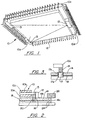
- Figs. 1 and 2 show a double-sided multichip module 10.
- a lid 10a covers integrated circuits and other components on the bottom of the module and lid 10b (visible in Fig. 2) covers components on the top of the module.
- the components are attached to the module's substrate 10c, which contains circuit vias (not shown, but well known) on the top surface to which wires or leads 12 are soldered for providing power and signal connections to the components.
- Thermal feet (pads) 13 are located in a triangular pattern on the bottom surface of the substrate 10c and adjacent to the perimeter of the lid 10a.
- Each foot is machined from 10Sn/90Pb (10% tin, 90% lead) solder blocks which are soldered to the conductive surface 10d on the bottom of the substrate 10c, vapor phase soldering being a preferred soldering technique.
- the three (3) feet create a "tripod" mount for the module 10.
- the module is placed on a printed wiring board 14 by soldering each foot to a conductive foot (pad) 16 on the top of the board, vapor phase soldering being a preferred technique.
- This is a "mass solder” reflow technique which employs the latent heat of condensation of an inert vapor, such as Flouronert® liquid available from Dupont to melt a solder past without apply excessive heat to circuit components.
- the printed wiring board 14 includes a conductive ground plane 18, and conductors 20 extend through the board 14 to connect the ground plane 18 and the conductive foot (pad) 16.
- the ground plane 18 extends to the edge 14a of the board 14 to a location in proximity to but electrically isolated from thermal vias 24 which provide a thermal path to a chassis wall 26.
- the wires 12 are soldered to the top 14a of the printed wiring board, again using vapor phase soldering.
- the multichip module is removed, for replacement, by melting the solder joints between the feet 13 and the module 10 and board 14 and the solder connections at the wires 12 using a process such as applying a stream of hot nitrogen gas to the solder joints.
- a plug 17 is used. Each of the feet 13 is soldered to the top of the plug.
- the plug is formed by first plating a hole 17a with a plating material 17b and then filling the interior volume with solder.
Landscapes
- Engineering & Computer Science (AREA)
- Microelectronics & Electronic Packaging (AREA)
- Manufacturing & Machinery (AREA)
- Combinations Of Printed Boards (AREA)
- Structures For Mounting Electric Components On Printed Circuit Boards (AREA)
Claims (3)
- Modul (10), das mindestens eine auf einem Substrat (10c) montierte Schaltungskomponente enthält, wobei das Substrat auf einer Leiterplatte (14) montiert ist, die eine Masseebene zur Verbindung mit einem Chassis und Umfangsleitungen aufweist, die die Komponente und die Leiterplatten verbinden, gekennzeichnet durch:wobei sich jeder der Füße in elektrischer und thermischer Verbindung mit der Masseebene (18) befindet.drei leitende, beabstandete Modulmontagefüße (13), die in einem dreieckigen Muster innerhalb der Leitungen auf einer Oberfläche des Substrats (10c) angeordnet sind, wobei jeder der Füße (13) leitend an dem Substrat (10c) und der Leiterplatte (14) angebracht ist;Montagepads (16) auf dem Substrat (10c) und der Leiterplatte (14) für die Füße; und
- Modul nach Anspruch 1, weiterhin gekennzeichnet durch die Füße (13) am Substrat (10c) anbringendes Lot, wobei jeder der Füße aus einem lötbaren Material mit einem Schmelzpunkt hergestellt ist, der höher liegt als der Schmelzpunkt des Lots.
- Verfahren zum Anbringen eines Moduls, das mindestens eine auf einem Substrat montierte Schaltungskomponente enthält, an einer Leiterplatte und Umfangsleitungen, die die Komponente mit der Leiterplatte verbindet, gekennzeichnet durch:das Anordnen thermisch und elektrisch leitender Füße in einem dreieckigen Muster zwischen dem Substrat und der Leiterplatte und innerhalb der Leitungen, um eine gewünschte Entfernung zwischen dem Substrat und der Leiterplatte bereitzustellen;Anbringen der Füße an den leitenden Pads auf der Leiterplatte, die mit einer Masseebene auf der Leiterplatte verbinden; undLöten der Füße an ein leitendes Pad auf dem Substrat durch einen Dampfphasenlötprozeß.
Applications Claiming Priority (2)
| Application Number | Priority Date | Filing Date | Title |
|---|---|---|---|
| US08/818,511 US5801923A (en) | 1997-03-14 | 1997-03-14 | Mounting multichip and single chip modules on printed wiring boards |
| US818511 | 1997-03-14 |
Publications (3)
| Publication Number | Publication Date |
|---|---|
| EP0865232A2 EP0865232A2 (de) | 1998-09-16 |
| EP0865232A3 EP0865232A3 (de) | 2000-01-19 |
| EP0865232B1 true EP0865232B1 (de) | 2003-08-27 |
Family
ID=25225713
Family Applications (1)
| Application Number | Title | Priority Date | Filing Date |
|---|---|---|---|
| EP98104452A Expired - Lifetime EP0865232B1 (de) | 1997-03-14 | 1998-03-12 | Montieren von Chip-Modulen auf gedruckten Leiterplatten |
Country Status (4)
| Country | Link |
|---|---|
| US (1) | US5801923A (de) |
| EP (1) | EP0865232B1 (de) |
| AT (1) | ATE248498T1 (de) |
| DE (1) | DE69817424T2 (de) |
Families Citing this family (1)
| Publication number | Priority date | Publication date | Assignee | Title |
|---|---|---|---|---|
| US6639801B2 (en) * | 2001-08-10 | 2003-10-28 | Agilent Technologies, Inc. | Mechanical packaging architecture for heat dissipation |
Family Cites Families (6)
| Publication number | Priority date | Publication date | Assignee | Title |
|---|---|---|---|---|
| US4748538A (en) * | 1985-07-08 | 1988-05-31 | Nec Corporation | Semiconductor module |
| US5142239A (en) * | 1991-05-20 | 1992-08-25 | Motorola, Inc. | High frequency linear amplifier assembly |
| US5109269A (en) * | 1991-07-08 | 1992-04-28 | Ofer Holzman | Method and means for positioning surface mounted electronic components on a printed wiring board |
| JP2509027B2 (ja) * | 1991-10-16 | 1996-06-19 | 三菱電機株式会社 | 半導体装置 |
| JPH0786717A (ja) * | 1993-09-17 | 1995-03-31 | Fujitsu Ltd | プリント配線板構造体 |
| US5508556A (en) * | 1994-09-02 | 1996-04-16 | Motorola, Inc. | Leaded semiconductor device having accessible power supply pad terminals |
-
1997
- 1997-03-14 US US08/818,511 patent/US5801923A/en not_active Expired - Lifetime
-
1998
- 1998-03-12 EP EP98104452A patent/EP0865232B1/de not_active Expired - Lifetime
- 1998-03-12 AT AT98104452T patent/ATE248498T1/de not_active IP Right Cessation
- 1998-03-12 DE DE69817424T patent/DE69817424T2/de not_active Expired - Fee Related
Also Published As
| Publication number | Publication date |
|---|---|
| EP0865232A2 (de) | 1998-09-16 |
| US5801923A (en) | 1998-09-01 |
| ATE248498T1 (de) | 2003-09-15 |
| EP0865232A3 (de) | 2000-01-19 |
| DE69817424D1 (de) | 2003-10-02 |
| DE69817424T2 (de) | 2004-07-08 |
Similar Documents
| Publication | Publication Date | Title |
|---|---|---|
| US5471368A (en) | Module having vertical peripheral edge connection | |
| JP2664873B2 (ja) | 電子パッケージおよびその作製方法 | |
| US6127204A (en) | Column grid array or ball grid array pad on via | |
| US6397459B2 (en) | Printed wiring board with mounted circuit elements using a terminal density conversion board | |
| US4750089A (en) | Circuit board with a chip carrier and mounting structure connected to the chip carrier | |
| JPH0677618A (ja) | 電子パッケージおよびその作成方法 | |
| JPH033290A (ja) | 電子回路アセンブリ用サーマルシヤント及びその製造方法 | |
| WO2000005936A1 (en) | Hybrid solder ball and pin grid array circuit board interconnect system and method | |
| KR100386018B1 (ko) | 스택형반도체디바이스패키지 | |
| US4964019A (en) | Multilayer bonding and cooling of integrated circuit devices | |
| US5198887A (en) | Semiconductor chip carrier | |
| EP1025748B1 (de) | Chipträgerelement und dessen verwendung | |
| US6452116B2 (en) | Use of blind vias for soldered interconnections between substrates and printed wiring boards | |
| KR100733684B1 (ko) | 소자의 전기 접촉을 위한 방법 및 장치 | |
| EP0865232B1 (de) | Montieren von Chip-Modulen auf gedruckten Leiterplatten | |
| US7615873B2 (en) | Solder flow stops for semiconductor die substrates | |
| US5880935A (en) | Device for using in an electronic controller | |
| JPH03798B2 (de) | ||
| US6033936A (en) | Method of mounting an LSI package | |
| EP0741507B1 (de) | Arrangement für integrierte Kreise und Methode zur Montierung davon | |
| JPS62244156A (ja) | 表面実装用パツケ−ジ | |
| JPH11214820A (ja) | Lccの実装構造 | |
| GB1504663A (en) | Large area hybrid microcircuit assembly | |
| JPS6224691A (ja) | チツプキヤリアの実装方法 | |
| JPH04342185A (ja) | 混成集積回路 |
Legal Events
| Date | Code | Title | Description |
|---|---|---|---|
| PUAI | Public reference made under article 153(3) epc to a published international application that has entered the european phase |
Free format text: ORIGINAL CODE: 0009012 |
|
| AK | Designated contracting states |
Kind code of ref document: A2 Designated state(s): AT BE CH DE DK ES FI FR GB GR IE IT LI LU MC NL PT SE |
|
| AX | Request for extension of the european patent |
Free format text: AL;LT;LV;MK;RO;SI |
|
| PUAL | Search report despatched |
Free format text: ORIGINAL CODE: 0009013 |
|
| AK | Designated contracting states |
Kind code of ref document: A3 Designated state(s): AT BE CH DE DK ES FI FR GB GR IE IT LI LU MC NL PT SE |
|
| AX | Request for extension of the european patent |
Free format text: AL;LT;LV;MK;RO;SI |
|
| 17P | Request for examination filed |
Effective date: 20000628 |
|
| AKX | Designation fees paid |
Free format text: AT BE CH DE DK ES FI FR GB GR IE IT LI LU MC NL PT SE |
|
| 17Q | First examination report despatched |
Effective date: 20010613 |
|
| GRAH | Despatch of communication of intention to grant a patent |
Free format text: ORIGINAL CODE: EPIDOS IGRA |
|
| GRAS | Grant fee paid |
Free format text: ORIGINAL CODE: EPIDOSNIGR3 |
|
| GRAA | (expected) grant |
Free format text: ORIGINAL CODE: 0009210 |
|
| AK | Designated contracting states |
Designated state(s): AT BE CH DE DK ES FI FR GB GR IE IT LI LU MC NL PT SE |
|
| PG25 | Lapsed in a contracting state [announced via postgrant information from national office to epo] |
Ref country code: NL Free format text: LAPSE BECAUSE OF FAILURE TO SUBMIT A TRANSLATION OF THE DESCRIPTION OR TO PAY THE FEE WITHIN THE PRESCRIBED TIME-LIMIT Effective date: 20030827 Ref country code: LI Free format text: LAPSE BECAUSE OF FAILURE TO SUBMIT A TRANSLATION OF THE DESCRIPTION OR TO PAY THE FEE WITHIN THE PRESCRIBED TIME-LIMIT Effective date: 20030827 Ref country code: FI Free format text: LAPSE BECAUSE OF FAILURE TO SUBMIT A TRANSLATION OF THE DESCRIPTION OR TO PAY THE FEE WITHIN THE PRESCRIBED TIME-LIMIT Effective date: 20030827 Ref country code: CH Free format text: LAPSE BECAUSE OF FAILURE TO SUBMIT A TRANSLATION OF THE DESCRIPTION OR TO PAY THE FEE WITHIN THE PRESCRIBED TIME-LIMIT Effective date: 20030827 Ref country code: BE Free format text: LAPSE BECAUSE OF FAILURE TO SUBMIT A TRANSLATION OF THE DESCRIPTION OR TO PAY THE FEE WITHIN THE PRESCRIBED TIME-LIMIT Effective date: 20030827 Ref country code: AT Free format text: LAPSE BECAUSE OF FAILURE TO SUBMIT A TRANSLATION OF THE DESCRIPTION OR TO PAY THE FEE WITHIN THE PRESCRIBED TIME-LIMIT Effective date: 20030827 |
|
| REG | Reference to a national code |
Ref country code: GB Ref legal event code: FG4D |
|
| REG | Reference to a national code |
Ref country code: CH Ref legal event code: EP |
|
| REG | Reference to a national code |
Ref country code: IE Ref legal event code: FG4D |
|
| REF | Corresponds to: |
Ref document number: 69817424 Country of ref document: DE Date of ref document: 20031002 Kind code of ref document: P |
|
| PG25 | Lapsed in a contracting state [announced via postgrant information from national office to epo] |
Ref country code: SE Free format text: LAPSE BECAUSE OF FAILURE TO SUBMIT A TRANSLATION OF THE DESCRIPTION OR TO PAY THE FEE WITHIN THE PRESCRIBED TIME-LIMIT Effective date: 20031127 Ref country code: GR Free format text: LAPSE BECAUSE OF FAILURE TO SUBMIT A TRANSLATION OF THE DESCRIPTION OR TO PAY THE FEE WITHIN THE PRESCRIBED TIME-LIMIT Effective date: 20031127 Ref country code: DK Free format text: LAPSE BECAUSE OF FAILURE TO SUBMIT A TRANSLATION OF THE DESCRIPTION OR TO PAY THE FEE WITHIN THE PRESCRIBED TIME-LIMIT Effective date: 20031127 |
|
| PG25 | Lapsed in a contracting state [announced via postgrant information from national office to epo] |
Ref country code: ES Free format text: LAPSE BECAUSE OF FAILURE TO SUBMIT A TRANSLATION OF THE DESCRIPTION OR TO PAY THE FEE WITHIN THE PRESCRIBED TIME-LIMIT Effective date: 20031208 |
|
| PG25 | Lapsed in a contracting state [announced via postgrant information from national office to epo] |
Ref country code: PT Free format text: LAPSE BECAUSE OF FAILURE TO SUBMIT A TRANSLATION OF THE DESCRIPTION OR TO PAY THE FEE WITHIN THE PRESCRIBED TIME-LIMIT Effective date: 20040127 |
|
| NLV1 | Nl: lapsed or annulled due to failure to fulfill the requirements of art. 29p and 29m of the patents act | ||
| PG25 | Lapsed in a contracting state [announced via postgrant information from national office to epo] |
Ref country code: LU Free format text: LAPSE BECAUSE OF NON-PAYMENT OF DUE FEES Effective date: 20040312 Ref country code: IE Free format text: LAPSE BECAUSE OF NON-PAYMENT OF DUE FEES Effective date: 20040312 |
|
| REG | Reference to a national code |
Ref country code: CH Ref legal event code: PL |
|
| PG25 | Lapsed in a contracting state [announced via postgrant information from national office to epo] |
Ref country code: MC Free format text: LAPSE BECAUSE OF NON-PAYMENT OF DUE FEES Effective date: 20040331 |
|
| ET | Fr: translation filed | ||
| PLBE | No opposition filed within time limit |
Free format text: ORIGINAL CODE: 0009261 |
|
| STAA | Information on the status of an ep patent application or granted ep patent |
Free format text: STATUS: NO OPPOSITION FILED WITHIN TIME LIMIT |
|
| 26N | No opposition filed |
Effective date: 20040528 |
|
| REG | Reference to a national code |
Ref country code: IE Ref legal event code: MM4A |
|
| PGFP | Annual fee paid to national office [announced via postgrant information from national office to epo] |
Ref country code: DE Payment date: 20060330 Year of fee payment: 9 |
|
| PG25 | Lapsed in a contracting state [announced via postgrant information from national office to epo] |
Ref country code: DE Free format text: LAPSE BECAUSE OF NON-PAYMENT OF DUE FEES Effective date: 20071002 |
|
| PGFP | Annual fee paid to national office [announced via postgrant information from national office to epo] |
Ref country code: IT Payment date: 20100320 Year of fee payment: 13 Ref country code: FR Payment date: 20100318 Year of fee payment: 13 |
|
| PGFP | Annual fee paid to national office [announced via postgrant information from national office to epo] |
Ref country code: GB Payment date: 20100208 Year of fee payment: 13 |
|
| GBPC | Gb: european patent ceased through non-payment of renewal fee |
Effective date: 20110312 |
|
| REG | Reference to a national code |
Ref country code: FR Ref legal event code: ST Effective date: 20111130 |
|
| PG25 | Lapsed in a contracting state [announced via postgrant information from national office to epo] |
Ref country code: FR Free format text: LAPSE BECAUSE OF NON-PAYMENT OF DUE FEES Effective date: 20110331 |
|
| PG25 | Lapsed in a contracting state [announced via postgrant information from national office to epo] |
Ref country code: GB Free format text: LAPSE BECAUSE OF NON-PAYMENT OF DUE FEES Effective date: 20110312 Ref country code: IT Free format text: LAPSE BECAUSE OF NON-PAYMENT OF DUE FEES Effective date: 20110312 |
|
| P01 | Opt-out of the competence of the unified patent court (upc) registered |
Effective date: 20230525 |