EP0859355B1 - Thin film magnetic head - Google Patents
Thin film magnetic head Download PDFInfo
- Publication number
- EP0859355B1 EP0859355B1 EP98102454A EP98102454A EP0859355B1 EP 0859355 B1 EP0859355 B1 EP 0859355B1 EP 98102454 A EP98102454 A EP 98102454A EP 98102454 A EP98102454 A EP 98102454A EP 0859355 B1 EP0859355 B1 EP 0859355B1
- Authority
- EP
- European Patent Office
- Prior art keywords
- layer
- gap insulative
- thin film
- magnetic head
- element portion
- Prior art date
- Legal status (The legal status is an assumption and is not a legal conclusion. Google has not performed a legal analysis and makes no representation as to the accuracy of the status listed.)
- Expired - Lifetime
Links
Images


Classifications
-
- C—CHEMISTRY; METALLURGY
- C23—COATING METALLIC MATERIAL; COATING MATERIAL WITH METALLIC MATERIAL; CHEMICAL SURFACE TREATMENT; DIFFUSION TREATMENT OF METALLIC MATERIAL; COATING BY VACUUM EVAPORATION, BY SPUTTERING, BY ION IMPLANTATION OR BY CHEMICAL VAPOUR DEPOSITION, IN GENERAL; INHIBITING CORROSION OF METALLIC MATERIAL OR INCRUSTATION IN GENERAL
- C23C—COATING METALLIC MATERIAL; COATING MATERIAL WITH METALLIC MATERIAL; SURFACE TREATMENT OF METALLIC MATERIAL BY DIFFUSION INTO THE SURFACE, BY CHEMICAL CONVERSION OR SUBSTITUTION; COATING BY VACUUM EVAPORATION, BY SPUTTERING, BY ION IMPLANTATION OR BY CHEMICAL VAPOUR DEPOSITION, IN GENERAL
- C23C16/00—Chemical coating by decomposition of gaseous compounds, without leaving reaction products of surface material in the coating, i.e. chemical vapour deposition [CVD] processes
- C23C16/02—Pretreatment of the material to be coated
- C23C16/0272—Deposition of sub-layers, e.g. to promote the adhesion of the main coating
-
- C—CHEMISTRY; METALLURGY
- C23—COATING METALLIC MATERIAL; COATING MATERIAL WITH METALLIC MATERIAL; CHEMICAL SURFACE TREATMENT; DIFFUSION TREATMENT OF METALLIC MATERIAL; COATING BY VACUUM EVAPORATION, BY SPUTTERING, BY ION IMPLANTATION OR BY CHEMICAL VAPOUR DEPOSITION, IN GENERAL; INHIBITING CORROSION OF METALLIC MATERIAL OR INCRUSTATION IN GENERAL
- C23C—COATING METALLIC MATERIAL; COATING MATERIAL WITH METALLIC MATERIAL; SURFACE TREATMENT OF METALLIC MATERIAL BY DIFFUSION INTO THE SURFACE, BY CHEMICAL CONVERSION OR SUBSTITUTION; COATING BY VACUUM EVAPORATION, BY SPUTTERING, BY ION IMPLANTATION OR BY CHEMICAL VAPOUR DEPOSITION, IN GENERAL
- C23C16/00—Chemical coating by decomposition of gaseous compounds, without leaving reaction products of surface material in the coating, i.e. chemical vapour deposition [CVD] processes
- C23C16/22—Chemical coating by decomposition of gaseous compounds, without leaving reaction products of surface material in the coating, i.e. chemical vapour deposition [CVD] processes characterised by the deposition of inorganic material, other than metallic material
- C23C16/26—Deposition of carbon only
-
- G—PHYSICS
- G11—INFORMATION STORAGE
- G11B—INFORMATION STORAGE BASED ON RELATIVE MOVEMENT BETWEEN RECORD CARRIER AND TRANSDUCER
- G11B5/00—Recording by magnetisation or demagnetisation of a record carrier; Reproducing by magnetic means; Record carriers therefor
- G11B5/127—Structure or manufacture of heads, e.g. inductive
- G11B5/31—Structure or manufacture of heads, e.g. inductive using thin films
- G11B5/3103—Structure or manufacture of integrated heads or heads mechanically assembled and electrically connected to a support or housing
- G11B5/3106—Structure or manufacture of integrated heads or heads mechanically assembled and electrically connected to a support or housing where the integrated or assembled structure comprises means for conditioning against physical detrimental influence, e.g. wear, contamination
-
- G—PHYSICS
- G11—INFORMATION STORAGE
- G11B—INFORMATION STORAGE BASED ON RELATIVE MOVEMENT BETWEEN RECORD CARRIER AND TRANSDUCER
- G11B5/00—Recording by magnetisation or demagnetisation of a record carrier; Reproducing by magnetic means; Record carriers therefor
- G11B5/127—Structure or manufacture of heads, e.g. inductive
- G11B5/33—Structure or manufacture of flux-sensitive heads, i.e. for reproduction only; Combination of such heads with means for recording or erasing only
- G11B5/39—Structure or manufacture of flux-sensitive heads, i.e. for reproduction only; Combination of such heads with means for recording or erasing only using magneto-resistive devices or effects
Definitions
- the present invention relates to a thin film magnetic head which can be employed for information processing devices such as personal computers or workstations, and which has a magnetoresistive element portion that moves over and relative to a magnetic writing or recording medium (hereinafter referred to as a recording medium), such as a hard or floppy disk, to read stored informations.
- a recording medium such as a hard or floppy disk
- Thin film magnetic heads have been conventionally employed in effecting high density recording of informations onto the recording medium.
- One example of such thin film magnetic heads is described in Japanese Patent Laying-open No. Hei 6-223331 (1994).
- Figure 7 is a schematic cross-sectional view of such a prior art magnetic head.
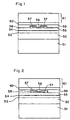
- the prior art thin film magnetic head has a substrate 1 on which an insulative layer 20 formed of diamond-like carbon (hereinafter referred to as DLC), a shielding layer 3, an insulative layer 21 formed of DLC, a magnetoresistive element portion (hereinafter referred to as an MR element layer 5), lead layers 6-A and 6-B, an insulative layer 22 formed of DLC, and a shielding layer 8 are stacked in such a consecutive order.
- DLC diamond-like carbon
- MR element layer 5 magnetoresistive element portion
- lead layers 6-A and 6-B an insulative layer 22 formed of DLC
- a shielding layer 8 is stacked in such a consecutive order.
- Figure 8 is a partly enlarged view of the MR element layer 5 and lead layers 6-A and 6-B in Figure 7.
- the MR element layer 5 has a nonmagnetic interlayer 11 sandwiched between a magnetoresistive layer 12 and a soft magnetic layer 10 which is closest of the three to the substrate 1.
- the soft magnetic layer 10 is a film for applying a bias electric field to the magnetoresistive layer 12.
- the nonmagnetic interlayer 11 is a film for magnetically isolating the soft magnetic layer 10 from the magnetoresistive layer 12 which is a film for converting magnetic flux changes to signals.
- Each of the lead layers 6-A and 6-B has an antiferromagnetic bias layer 13 on which an adherence enhancing layer 14 and a conductive lead layer 15 are consecutively stacked.
- the lead layers 6-A and 6-B define an operational region 6-C therebetween.
- a rated current is applied to the lead layer 6-A to allow the rated current to flow therefrom through the MR element layer 5 to the lead layer 6-B.
- the current flowing into the MR element layer 5 produces an electric field perpendicular to a direction of the current flow, inducing magnetic fields in the magnetoresistive layer 12 as well as the soft magnetic layer 10, so that the magnetoresistive layer 12 is biased in the direction of the current flow through a coupling effect.
- the magnetoresistive layer 12 When subjected to an external magnetic field while in such a biased state, the magnetoresistive layer 12 changes in its resistance with varying magnetic field. The output can be obtained by processing the resistance changes as signals.
- DLCs are generally high in internal stress, particularly in compressive stress. Due to the action of this compressive stress, a tensile force acts to a body adhered to the DLC.
- the lead layers 6-A and 6-B, as well as the MR element layer 5, are sandwiched between the insulative layers 21 and 22. Accordingly, the compressive forces generated in the insulative layers 21 and 22 are likely to act to deform the MR element layer 5, leading to failure of obtaining desired electrical characteristics and, as a consequence, loss of reliability.
- forming the insulative layers having a high compressive stress directly on the shielding layers, as described above, is very likely to cause upper layers including the insulative layers to be delaminated from the substrate when subjected to the action of compressive forces in the insulative layers.
- EP 0 584 707 being refleted in the preambles of claims 1, 2, 19 and 20 relates to a wear-resistant thin-film magnetic head assembly and method of making same.
- the head assembly includes a wear-resistant layer of diamond-like carbon and a substrate of titanium carbide particles dispersed in an alumina matrix. Adhesion of the diamond-like carbon to the substrate is improved by depositing an adhesion promoting layer on the substrate. A second adhesion promoting layer can be deposited onto the diamond-like carbon layer to facilitate the deposition of electromagnetic circuitry on the diamond-like carbon layer. Diamond-like carbon can be used as an insulater anywhere inside the head assembly.
- EP 0 584 707 simplifies the construction of head assembly and increases its resistance to wear by moving magnetic media, but does not disclose a structure, wherein an upper gap insulative layer has an internal stress lower than that of a lower gap insulative layer.
- JP 05274626 discloses the forming of an magnetoresistive element in such a manner that the element hardly receives the deformation by the internal stress of insulating films enclosing the element. But neither an interlayer disposed between the lower gap insulative layer and the lower shielding layer or between the the upper gap insulative layer and the magnetoresistive element portion nor an internal stress relaxation layer is disclosed.
- US 4,728,529 relates to a method of producing diamond-like carbon coatings in which hydrocarbons and hydrogen, possible in the presence of a nobel gas, are ionized by plasma discharge. In this way diamond-like, transparent, clear and uncolored carbon coatings with low internal stresses are generated on substrates.
- JP 03028195 discloses a method for forming a diamond-like carbon film on a substrate, the stress generated in that diamond-like carbon film being remarkably decreased compared with conventional method by intermittently introducing a hydrocarbon gas into a reaction chamber.
- a magnetic head in accordance with a first aspect of the invention characteristically includes a magnetoresistive element portion (MR element portion) movable over and relative to a magnetic recording medium for reading informations stored therein, upper and lower shielding layers disposed to locate the magnetoresistive element portion therebetween for magnetically shielding the magnetoresistive element portion, and upper and lower gap insulative layers respectively interposed between the upper shielding layer and the magnetoresistive element portion and between the lower shielding layer and the magnetoresistive element portion.
- MR element portion magnetoresistive element portion
- upper and lower shielding layers disposed to locate the magnetoresistive element portion therebetween for magnetically shielding the magnetoresistive element portion
- upper and lower gap insulative layers respectively interposed between the upper shielding layer and the magnetoresistive element portion and between the lower shielding layer and the magnetoresistive element portion.
- each of the upper and lower gap insulative layers comprises a hydrogen-incorporated film, characterized in that said upper gap insulative layer has an internal stress lower than that of said lower gap insulative layer and that an interlayer is disposed between said lower gap insulative layer and said lower shielding layer.
- the hydrogen-incorporated film for each of the upper and lower gap insulative layers is preferably a hydrogenated amorphous carbon film.
- the hydrogenated amorphous carbon film is the one which is generally called as a diamond-like carbon film (DLC film).
- a silicon film can be employed to form a hydrogen-incorporated film for each of the upper and lower gap insulative layers. Since the DLC and silicon films are excellent in thermal conductivity, they dissipate heat very quickly to prevent excessive temperature elevation in the MR element portion so that a service life of the MR element portion can be prolonged.
- the DLC film Generally for the DLC film, its internal stress and hardness tend to decrease with increasing hydrogen content thereof. Accordingly, as the hydrogen content of the upper gap insulative layer is rendered higher compared to that of the lower gap insulative layer, the upper gap insulative layer will exhibit a reduced internal stress and a reduced hardness relative to the lower gap insulative layer.
- the film layers of the thin film magnetic head are consecutively stacked on a substrate, respectively by a thin film forming method.
- the formation of the MR element portion follows that of the lower gap insulative layer but precedes that of the upper gap insulative layer.
- the internal stress of the upper gap insulative layer generally exerts greater influence upon the MR element portion relative to that of the lower gap insulative layer. Therefore, the service life of the MR element portion can be effectively prolonged to result in its increased reliability by designing the upper gap insulative layer as having a decreased internal stress relative to the lower gap insulative layer.
- one of the upper and lower gap insulative layers can be reduced in hardness relative to the other by differentiating the hydrogen contents thereof from each other.
- the wear-resistance of the MR element portion, interposed between the upper and lower gap insulative layers can be increased by imparting increased hardness to either one of the gap insulative layers. Since the upper gap insulative layer has a decreased internal stress relative to the lower gap insulative layer, as described above, it is preferred to design the lower gap insulative layer as having an increased hardness relative to the upper gap insulative layer.
- a magnetic head in accordance with a second aspect of the invention includes a magnetoresistive element portion (MR element portion) movable over and relative to a magnetic recording medium for reading informations stored therein, upper and lower shielding layers disposed to locate the magnetoresistive element portion therebetween for magnetically shielding the magnetoresistive element portion, and upper and lower gap insulative layers respectively interposed between the upper shielding layer and the magnetoresistive element portion and between the lower shielding layer and the magnetoresistive element portion.
- MR element portion magnetoresistive element portion
- upper and lower shielding layers disposed to locate the magnetoresistive element portion therebetween for magnetically shielding the magnetoresistive element portion
- upper and lower gap insulative layers respectively interposed between the upper shielding layer and the magnetoresistive element portion and between the lower shielding layer and the magnetoresistive element portion.
- each of the upper and lower gap insulative layers comprises a hydrogen-incorporated film, characterized in that said upper gap insulative layer has an internal stress lower than that of said lower gap insulative layer and that an interlayer is disposed between said upper gap insulative layer and said magnetoresistive element portion.
- the internal stress of the upper gap insulative layer is lower than that of the lower gap insulative layer. This enables a reduced influence of the internal stress upon the MR element portion to result in a highly reliable thin film magnetic head having a prolonged service life.
- the internal stress of the upper gap insulative layer is preferably in the range of 0.01 - 4 GPa while the internal stress of the lower gap insulative layer is preferably in the range of 4 - 10 GPa.
- the lower gap insulative layer will exhibit increased hardness relative to the upper gap insulative layer.
- the hydrogen-incorporated film for each of the upper and lower gap insulative layers preferably comprises a hydrogenated amorphous carbon film, as similar to those in the first aspect of the present invention.
- a silicon film can be employed to form the hydrogen-incorporated film for each of the upper and lower gap insulative layers.
- the hydrogen content of the upper gap insulative layer is rendered higher than that of the lower gap insulative layer.
- each of said upper and lower gap insulative layers is comprised of a hydrogenated amorphous carbon film
- this amorphous hydrogenated carbon film may contain at least one element selected from Si, B, N and O.
- the incorporation of Si, B, N or 0 improves sliding characteristics thereof while the incorporation of N serves to reduce an internal stress therein.
- the content of incorporated element(s) preferably ranges from 2 to 80 atomic percent.
- an interlayer is disposed between the lower gap insulative layer and the lower shielding layer.
- the provision of such an interlayer serves to improve adhesion of the lower gap insulative layer.
- the above interlayer is either alternatively or additionally disposed between the upper gap insulative layer and the magnetoresistive element portion.
- the provision of this interlayer serves to improve adhesion of the upper gap insulative layer.
- the interlayer may be provided either in such a continuous film form as coexpansive with the neighboring layers or in such an intermittent form as consisting of plural island portions sandwiched between the neighboring layers.
- a film thickness of the interlayer is preferably not greater than 200 ⁇ . Also, the film thickness of the interlayer is preferably not greater than one fifth of a film thickness of corresponding upper or lower gap insulative layer.
- the interlayer can be formed of Si, Ru, Mo, W, Cr, C, Ge, Hf, Zr, or Ti. Any of those elements each combined with at least one element selected from nitrogen, oxygen and carbon may also be employed to form the interlayer.
- an internal stress relaxation layer may be included therein.
- Such an internal stress relaxation layer may be incorporated in plurality within the amorphous carbon film.
- the internal stress relaxation layer can be formed of a carbon film containing substantially no hydrogen, for example.
- a carbon film containing substantially no hydrogen may be formed such as by sputtering.
- the internal stress relaxation layer can be formed of Si, Ru, Mo, W, Cr, Ge, Hf, Zr or Ti. Any of those elements each combined with at least one element selected from nitrogen, oxygen and carbon may also be employed to form the internal stress relaxation layer.
- the above amorphous carbon film incorporating the internal stress relaxation layer(s) comprises a plurality of carbon layers having an equivalent thickness a alternating with a plurality of internal stress relaxation layers having an equivalent thickness b.
- the ratio a/b is preferably in the range of 1 - 1000, more preferably in the range of 10 - 500.
- Such a carbon layer specifically in surface contact with the internal stress relaxation layer is hereinafter referred to simply as a carbon layer.
- a ratio in hardness of each carbon layer to each internal stress relaxation layer is preferably not less than 10.
- a ratio in internal stress of each carbon layer to each internal stress relaxation layer is preferably not less than 100.
- the film thickness a of each carbon layer preferably ranges from about 50 ⁇ to about 5 ⁇ m, more preferably from about 100 ⁇ to about 1 ⁇ m.
- the film thickness b of each internal stress relaxation layer preferably ranges from about 5 ⁇ to about 5 ⁇ m, more preferably from about 10 ⁇ to about 1 ⁇ m.
- the presence of the internal stress relaxation layer(s) interior of the amorphous carbon film acts to relax internal stresses in the carbon layers flanking the internal stress relaxation layer, so that a total internal stress of the amorphous carbon film can be effectively reduced.
- such an internal stress relaxation layer may be incorporated at least in the upper gap insulative layer, since the internal stress of the upper gap insulative layer is preferred as being smaller than that of the lower gap insulative layer.
- the hydrogen content of the upper or/and lower gap insulative layer is preferably in the range of 5 - 65 atomic percent. Also, 25 % or greater of carbon-carbon bonds present in the upper or/and lower gap insulative layer is preferably occupied by sp 3 carbon-carbon bonds.
- the internal stress of the upper or/and lower gap insulative layer is preferably in the range of 0.5 - 9.0 GPa. Also, a specific resistance of the upper or/and lower gap insulative layer is preferably in the range of 10 9 - 10 12 ⁇ cm.
- a thin film magnetic head in accordance with the third aspect of the present invention includes a magnetoresistive element portion movable over and relative to a magnetic recording medium for reading information stored therein; upper and lower shielding layers disposed to locate said magnetoresistive element portion therebetween for magnetically shielding the magnetoresistive element portion; and upper and lower gap insulative layers respectively interposed between said upper shielding layer and the magnetoresistive element portion and between said lower shielding layer and the magnetoresistive element portion, each of said upper and lower gap insulative layers comprising a hydrogen-incorporated film, characterized in that said upper gap insulative layer has an internal stress lower than that of said lower gap insulative layer and that at least one of said upper and lower gap insulative layers includes an internal stress relaxation layer which is formed of Si, Ru, Mo, W, Cr, Ge, Hf, Zr or Ti, or any of those elements each combined with at least one element selected from nitrogen, oxygen and carbon.
- a thin film magnetic head in accordance with the fourth aspect of the present invention includes a magnetoresistive element portion movable over and relative to a magnetic recording medium for reading informations stored therein, upper and lower shielding layers disposed to locate the magnetoresistive element portion therebetween for magnetically shielding the magnetoresistive element portion, and upper and lower gap insulative layers respectively interposed between the upper shielding layer and the magnetoresistive element portion and between the lower shielding layer and the magnetoresistive element portion.
- the thin film magnetic head further includes a first interlayer disposed between the lower gap insulative layer and the lower shielding layer, and a second interlayer disposed between the upper gap insulative layer and the magnetoresistive element portion wherein each of said first and second interlayer is formed of Si, Ru, Mo, W, Cr, C, Ge, Hf, Zr or Ti, or any of those elements each combined with at least one element selected from nitrogen, oxygen and carbon.
- each of the upper and lower gap insulative layers preferably comprises a hydrogenated amorphous carbon film, as similar to the first, second and third aspects of the present invention.
- the first and second interlayers are preferably analogous to those in accordance with the first and second aspects of the present invention.
- One embodiment of a thin film magnetic head in accordance with the present invention can be manufactured according to the following steps (1) through (9) which will be explained below referring to Figure 1.
- the second, third, sixth and seventh steps can be performed, such as by an ECR plasma generator shown in Figure 5.
- the wafer is transferred to another film forming means, e.g. sputtering means, in which the processes of the fourth and fifth steps are carried out. Thereafter, the wafer is again returned to the ECR plasma generator shown in Figure 5 in which the subsequent processes are carried out.
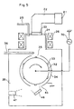
- Figure 5 is a schematic cross-sectional view of an exemplary apparatus for forming, on the wafer, the first interlayer (formed according to the second step), the second interlayer (formed according to the sixth step), the lower gap insulative layer (formed according to the third step) and the upper gap insulative layer (formed according to the seventh step).
- a plasma generation chamber 24 is arranged within a vacuum chamber 28 to which one end of a waveguide 22 is connected. Another end of the waveguide 22 is mounted to a microwave supplying means 21. Microwaves generated in the microwave supplying means 21 pass through the waveguide 22 and a microwave inlet window 23 to be guided into the plasma generation chamber 24.
- a discharge gas inlet line 25 for introducing a discharge gas, such as an argon (Ar) gas, into the plasma generation chamber 24.
- a discharge gas such as an argon (Ar) gas
- a plurality of plasma magnetic field generators 26 is mounted circumferentially of the plasma generation chamber 24. The interaction of a high-frequency magnetic field induced by the microwaves and a magnetic field from the plasma magnetic field generators 26 generates a high-density plasma within the plasma generation chamber 24.
- a drum-shaped substrate holder 32 is provided within the vacuum chamber 28 so as to be rotatable about an axis (located perpendicular relative to a sheet surface of the drawing) disposed perpendicular to a wall surface of the vacuum chamber 28.
- a plurality of wafers 33 are arranged circumferentially of the substrate holder 32 at regular intervals, and a high-frequency power source 30 is connected to the substrate holder 32.
- a hollow cylindrical shielding cover 34 made of metal, radially surrounds the substrate holder 32 to define therebetween a space of predetermined dimension.
- This shielding cover 34 is connected to a grounded electrode.
- This shielding cover 34 is mounted for the purpose of preventing generation of discharges between the vacuum chamber 28 and a substrate holder area excluding target film-forming locations thereon, which discharges will be otherwise generated when an RF voltage is applied to the substrate holder 32 for film formation.
- the shielding cover 34 has a first opening 35 through which a plasma from the plasma generation chamber 24 is directed to the wafers 33 mounted on the substrate holder 32.
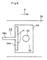
- the vacuum chamber 28 incorporates a reaction gas inlet line 36, and a leading end of the reaction gas inlet line 36 is positioned above the first opening 35.
- Figure 6 is a plan view showing this leading end of the reaction gas inlet line 36 and its vicinity.
- the reaction gas inlet line 36 includes a gas inlet portion 36a for introducing a raw material gas, such as a CH 4 gas, into the vacuum chamber 28 from external, and a gas discharge portion 36b for perpendicular connection to the gas inlet portion 36a.
- a raw material gas such as a CH 4 gas
- the gas discharge portion 36b is arranged to perpendicularly cross a rotational direction A of the substrate holder 32, and is positioned above the first opening 35. In the plan view, the gas discharge portion 36b is located upstream along the rotational direction A within the opening 35.
- the gas discharge portion 36b has plural holes 41 each directed downwardly at an angle of about 45 degrees. In this embodiment, eight holes 41 are provided.
- the shielding cover 34 has at its bottom a second opening 43 which vertically faces the first opening 15.
- a target 46 comprised of material atoms constituting the first interlayer 54 and the second interlayer 58.
- an ion gun 47 Disposed in the vicinity of the target 46 is an ion gun 47 which directs ions in an inert gas to the target 46 for sputtering the target 46.
- an Ar gas is employed as the inert gas.
- the target 46 and the ion gun 47 serve to pass the material atoms constituting the first interlayer 54 or the second interlayer 58 through the second opening 43 to be discharged onto the wafers 33.
- the apparatus of Figure 5 was employed to form, on a wafer, Si layers as a first interlayer 54 and a second interlayer 58, as well as hydrogenated amorphous carbon films as a lower gap insulative layer 55 and an upper gap insulative layer 59.
- the vacuum chamber 28 was evacuated to a pressure of 10 -5 -10 -4 Torr. , followed by rotation of the substrate holder 32 at a speed of about 10 rpm. Then, an Ar gas was supplied to the ion gun 47 to obtain Ar ions which were directed onto a surface of the Si target 46, wherein an acceleration voltage and ionic current density of the Ar ions was set at 900 eV and at 0.4 mA/cm 2 , respectively.
- the above process was continued for about 1 minute to form, on a surface of a shielding layer 53, the first Si interlayer 54 to a thickness of 20 ⁇ .
- the emission of Ar ions was then discontinued to commence supplying the Ar gas at 5.7 x 10 -4 Torr. from the ECR plasma generating apparatus.
- the microwave supplying means 21 supplied a 2.45 GHz microwave at 200 W to produce an Ar plasma within the plasma generation chamber 24.
- the produced Ar plasma was passed through the first opening 35 and directed onto a surface of the first interlayer 54.
- the high-frequency power source 30 applied a 13.56 MHz RF voltage to the substrate holder 32 to cause a wafer 33 to produce a self-bias voltage, while the reaction gas inlet line 36 supplied a CH 4 gas at 1.0 x 10 -3 Torr., to thereby form a hydrogenated amorphous carbon film (DLC film).
- DLC film hydrogenated amorphous carbon film
- the lower gap insulative layer 55 was formed, on the first interlayer 54, to a thickness of 1000 ⁇ .
- the similar process was further repeated to form the second interlayer 58 of 20 ⁇ thickness, and successively to form the upper gap insulative layer 59 of 1000 ⁇ thickness on the second interlayer 58.
- a thin film magnetic head was thus prepared (EXAMPLE 1).
- a lower gap insulative layer 55 was formed, on a first interlayer 54 (20 ⁇ thick), to a thickness of 400 ⁇
- an upper gap insulative layer 59 was formed, on a second interlayer 58 (20 ⁇ thick), to a thickness of 400 ⁇ to prepare a thin film magnetic head (EXAMPLE 2).
- Figure 2 shows an exemplary modification of the thin film magnetic head of Figure 1.
- the thin film magnetic head of Figure 2 is identical to that of Figure 1, except that a second interlayer 58 was formed on an MR element layer 56 and an electrode layer 57, exclusively.
- Such a modified thin film magnetic head can be prepared in the same manner as employed in preparing the thin film magnetic head of Figure 1, with the exception that after the second interlayer 58 was formed to expand on the lower gap insulative layer 55, the MR element layer 56 and the electrode layer 57, a portion of the second interlayer 58 formed on the lower gap insulative layer 55 was etched for removal.
- Figure 3 is a graph showing the internal stress and hydrogen content in the hydrogenated amorphous carbon film of 1000 ⁇ thickness, as used for each of the lower gap insulative layer 55 and upper gap insulative layer 59, in relation to the self-vias voltage.
- the concentration of hydrogen incorporated in the hydrogenated amorphous carbon film, as well as its internal stress, are controlled by varying the self-bias voltage. That is, as the self-bias voltage increases, the concentration of hydrogen incorporated in the hydrogenated amorphous carbon film decreases while its internal stress increases. It therefore becomes possible to predict the internal stress by determining the concentration of hydrogen incorporated in the film.
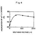
- Figure 4 shows the sp 3 bonding between carbon atoms contained in the hydrogenated amorphous carbon film in relation to the self-bias voltage.
- a hydrogenated amorphous carbon film having a high internal stress (high-stress film), a hydrogenated amorphous carbon film having a low internal stress (low-stress film) and an Al 2 O 3 film were respectively formed each to a thickness of 1000 ⁇ to determine their internal stresses and hardnesses.
- the self-bias voltages applied when forming the above films, as well as internal stresses and hardnesses of the films formed, are given in Table 1. High Stress Film Law Stress Film Al 2 O 3 Film Self-Bias Voltage -50V -10V --- Internal Stress (Film Thickness of 1000 ⁇ ) 6.5Gpa 3.2GPa 1.1GPa Vickers Hardness 3000 1000 800
- the internal stress of film can be determined generally from the degree of deformation of a substrate.
- the internal stress can be evaluated by determining a degree of deflection which appears when the film is formed on the substrate while allowing the stress produced to be exerted thereon, and which depends on the shape and elastic constant of the substrate. This technique is referred to as "deflection method" (Stress Physics, Vol.66, No.7 (1987), pp. 923-924), and was employed to determine the internal stress of the films shown in Table 1.
- the films having different internal stresses given in Table 2 were formed for the lower gap insulative layer 55 and the upper gap insulative layer 59 to prepare five types of thin film magnetic heads; those prepared in Example 1, Example 2, and Comparative Examples 1 through 3.
- the power-applied life test was conducted. In addition, they were subjected to a sliding test with a recording medium for a given time period for subsequent determination of the wear amount of the MR element layer 56.
- the results are given in Table 2.
- those superior to Comparable Example 3 are indicated by the rating of o ⁇ , and those comparable to Comparable Example 3 by the rating of ⁇ .
- the life test was carried out by allowing a current to flow through the MR element layer 56 and determining the service life until the current value fell below a specified value.
- Comparative Example 1 is comparable in power applied service life to Comparative Example 3, but Examples 1 and 2, as well as Comparative Example 2, are superior in power applied service life to Comparative Example 3.
- those in Examples 1 and 2 are one fourth or less of that in Comparative Example 3 and smaller than that in Comparative Example 2.
- Example 4 For each of the thin film magnetic heads prepared in Example 1, Example 2 and Comparative Example 3, the current was measured which leaked from the MR element layer 56 into the shielding layer 53.
- each of the upper and lower gap insulative layers was made from an Al 2 O 3 film of 400 ⁇ thickness to prepare a thin film magnetic head (Comparative Example 4) which was also measured for its leak current.
- Table 3 Exp. 1 Exp. 2 Comp. Exp. 3 Comp. Exp. 4 Material for Upper and Lower Gap Insulative Layers Hydrogenated Amorphous Carbon Film Al 2 O 3 Film Film Thickness of Upper and Lower Gap Insulative Layers ( ⁇ ) 1000 400 1000 400 Leak Current From MR Element Layer to Shielding Layer 17 27 100 374
- the respective components of the lower gap insulative layer 55 and the upper gap insulative layer 59 are not limited to those used in the above Examples, and may contain a suitable amount of impurities such as Si, B, N or O to improve their sliding characteristics or the others.
- any material, other than Si, can be employed for the first interlayer 54 and the second interlayer 58, so far as its use serves to improve the adhesion between the lower gap insulative layer 55 and an underlying layer of the first interlayer 54, and between the upper gap insulative layer 59 and an underlying layer(s) of the second interlayer 54.
- Si was used in the above-described Examples for each of the first interlayer 54 and the second interlayer 58
- other materials can be employed which include Ru, Mo, W, Cr, C, Ge, Hf, Zr or Ti, or alternatively, any of those elements each combined with at least one element selected from nitrogen, oxygen and carbon can be employed. Those materials were confirmed as providing as similar results as Si by experiments.
- the temperatures at which the films were formed under the above-described film-forming conditions to respectively constitute the lower and upper gap insulative layers were confirmed as being not higher than 100 °C by experiments.
- the above-described Examples varied the self-bias voltage as a technique of controlling the internal stress, it is not limiting.
- the internal stress of a film can be controlled by incorporating nitrogen in the film, for example.
- a nitrogen-incorporated, hydrogenated amorphous carbon film can be formed by setting the pressures of CH 4 and N 2 gases at 1 x 10 -3 Torr. and 5.7 x 10 -4 Torr., respectively, under the film-forming condition shown in Table 1 for the high stress film.
- the resulting film had an internal stress of 3.9 GPA and a Vickers hardness of 2800 Hv. Therefore, the incorporation of nitrogen into the hydrogenated amorphous carbon film imparts an increased hardness and reduced internal stress thereto.
- an internal stress relaxation layer may be disposed interior thereof. Such a method will be explained below.
- Figure 9 is a schematic cross-sectional view of a hydrogenated amorphous carbon film which incorporates the internal stress relaxation layer and which can be employed to constitute the upper or/and lower gap insulative layer according to the present invention.
- the hydrogenated amorphous carbon film 74 includes carbon layers 72 alternating with internal stress relaxation layer 73. This provision of an internal stress relaxation layer(s) in the hydrogenated amorphous carbon film serves to reduce the internal stress of the hydrogenated amorphous carbon film.
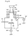
- FIG 10 is a schematic cross-sectional view showing an exemplary apparatus for forming the hydrogenated amorphous carbon film incorporating the internal stress relaxation layer.
- This thin film forming apparatus enables a thin film formation by both or either of an ECR plasma CVD technique and a sputtering technique.
- a plasma generation chamber 84, as well as a reaction chamber (now shown) for locating a substrate 88 therein, are disposed in a vacuum chamber 87.
- a waveguide 82 connects the plasma generation chamber 84 to a microwave generator 81.
- a microwave inlet window 83 is disposed at the connection of the waveguide 82 and the plasma generation chamber 84.
- a discharge gas inlet line 85 for introducing a discharge gas, such as an argon (Ar) gas, into the plasma generation chamber 84.
- a plasma magnetic field generator 86 is further disposed to radially surround the plasma generation chamber 84.
- a substrate holder 89 Disposed interior of the reaction chamber within the vacuum chamber 87 is a substrate holder 89 on which placed is the substrate 88.
- a reaction gas inlet line 91 Connected to the reaction chamber within the vacuum chamber 87 is a reaction gas inlet line 91 for introducing a reaction gas which serves as a raw material gas in the plasma CVD method.
- a high-frequency power source 90 Connected to the substrate holder 89 is a high-frequency power source 90 for producing a self-bias voltage in the substrate 88.
- a sputter source 92 mounting a target for forming a thin film on the substrate 88 through a sputtering technique.
- a high-frequency power source 93 is further provided for supplying a high-frequency power to the sputter source 92.
- the vacuum chamber 87 is evacuated through an air outlet 94 to a predetermined pressure.
- a carbon film shown in Figure 9 was formed employing the thin film forming apparatus of Figure 10.
- the following Process 1 for forming a carbon layer and Process 2 for forming an internal stress relaxation layer were repeated alternately to form the carbon film.
- a graphite target was employed to sputter form an amorphous carbon film containing substantially no hydrogen which serves as the internal stress relaxation layer.
- the substrate 88 is mounted on the substrate holder 89 and the vacuum chamber 87 is evacuated to a pressure of 10 -5 ⁇ 10 -7 Torr. Then, the Ar gas at 5.7 x 10 -4 Torr. is introduced, through the discharge gas inlet line 85, to the plasma generation chamber 84, and concurrently a microwave at 2.45 GHz and 100 W is supplied from the microwave generator 81 into the plasma generation chamber 84 to produce, within the plasma generation chamber 84, an Ar plasma which is subsequently directed onto a surface of the substrate 88.
- a reaction gas inlet line 91 supplies a CH 4 gas at 7.6 x 10 -4 Torr.
- the CH 4 gas supplied from the reaction gas inlet line 91 is decomposed by the action of the plasma to produce carbons which become highly reactive carbon ions or neutral active carbons for acceleration onto the surface of the substrate 88.
- the high-frequency power source 90 applies a 13.56 MHz RF power to the substrate holder 89 so that the substrate 88 produces a self-bias voltage of -50 V.
- a carbon layer is formed to a thickness of 900 ⁇ by a single film-forming process.
- the CH 4 gas supply from the reaction gas inlet line 91 is terminated to commence supplying the Ar gas at 1 x 10 -3 Torr. from the discharge gas inlet line 85.
- the high-frequency power source 93 applies a 13.56 MHz RF power to the sputter source 92 for actuation thereof.
- an amorphous carbon film layer of 100 ⁇ thickness is formed on the substrate 88 to serve as the internal stress relaxation layer.
- Process 1 and Process 2 were alternately repeated ten times each and finally Process 1 was carried out once. Accordingly, ten sets of a unit comprised of the carbon layer 72 and the internal stress relaxation layer 73 were consecutively layered, and one additional carbon layer 72 was finally stacked thereon to provide a carbon film 74 of a total of twenty one layers, as shown in Figure 9. An overall thickness of this carbon film 74 was 1.09 ⁇ m.
- the above Process 2 was followed to form an amorphous carbon layer, i.e. a thin film of 1.09 ⁇ m thickness.
- Example 3 The films obtained respectively in Example 3 and Comparative Examples 5 and 6 were measured for Vickers hardness and internal stress. The results are given in Table 4. Exp. 3 Comp. Exp. 5 Comp. Exp. 6 Vickers Hardness 3000 3100 270 Internal Stress 0.72 1.0 0.01
- the carbon film obtained in Example 3 exhibits a Vickers hardness comparable to that of the carbon layer, i.e. a diamond-like carbon film obtained in Comparative Example 5, but exhibits a decreased internal stress compared to the diamond-like carbon film obtained in Comparative Example 5.
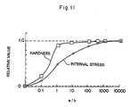
- Figure 11 is a graph showing the Vickers hardness and internal stress of a carbon film when the ratio a/b of the film thickness a of the carbon layer to the film thickness b of the internal stress relaxation layer is varied.
- the values of the Vickers hardness and internal stress given in the graph indicates the relative values when the Vickers hardness and internal stress of the film obtained in Comparative Example 5 were respectively taken as 1.
- the measured carbon film was a multilayer film including eleven carbon layers and ten internal stress relaxation layers and had an overall thickness of 1.09 ⁇ m, as identical to the carbon film obtained in Example 3.
- the carbon film exhibits a comparable hardness and a reduced internal stress relative to the diamond-like carbon film obtained in Comparative Example 3 when the ratio a/b of film thicknesses is within the range of 1 ⁇ 1000, and a similarly comparable hardness and a further reduced internal stress relative to the diamond-like carbon film obtained in Comparative Example 3 when the ratio a/b of film thicknesses is within the range of 10 ⁇ 500.
- Step 1 and Step 2 according to Example 3 were followed, except that in Step 2, a sputter source 92 mounting an Si target was employed to sputter form the Si layer of about 100 ⁇ thickness which served as the internal stress relaxation layer. As a result, a carbon layer was obtained which included the Si layer stacked on the carbon layer.
- the carbon film obtained was measured for Vickers hardness and internal stress.
- the Vickers hardness was 3050 Hv.
- the relative value of its internal stress was 0.75 when the measured internal stress of the diamond-like film obtained in Comparative Example 5 was taken as 1.
- a W layer was formed as an internal stress relaxation layer.
- Step 1 and Step 2 according to Example 3 were followed, except that in Step 2, a sputter source 92 mounting a W target was employed to sputter form the W layer of about 100 ⁇ thickness which served as the internal stress relaxation layer.
- a carbon layer was obtained which included the W layer stacked on the carbon layer.
- the carbon film obtained was measured for Vickers hardness and internal stress.
- the Vickers hardness was 3000 Hv.
- the relative value of its internal stress was 0.73 when the measured internal stress of the diamond-like film obtained in Comparative Example 5 was taken as 1.
- a Zr layer was formed as an internal stress relaxation layer. Step 1 and Step 2 according to Example 3 were followed, except that in Step 2, a sputter source 92 mounting a Zr target was employed to sputter form the Zr layer of about 100 ⁇ thickness which served as the internal stress relaxation layer. As a result, a carbon layer was obtained which included the Zr layer stacked on the carbon layer.
- the carbon film obtained was measured for Vickers hardness and internal stress.
- the Vickers hardness was 3000 Hv.
- the relative value of its internal stress was 0.73 when the measured internal stress of the diamond-like film obtained in Comparative Example 5 was taken as 1.
- Step 1 and Step 2 according to Example 3 were followed, except that in Step 2, a sputter source 92 mounting an SiC target was employed, and a CH 4 gas at 9.5 x 10 -5 Torr. was supplied from the reaction gas inlet line 91 to sputter form the SiC layer of about 100 ⁇ thickness which served as the internal stress relaxation layer. As a result, a carbon layer was obtained which included the SiC layer stacked on the carbon layer.
- the carbon film obtained was measured for Vickers hardness and internal stress.
- the Vickers hardness was 3080 Hv.
- the relative value of its internal stress was 0.8 when the measured internal stress of the diamond-like film obtained in Comparative Example 5 was taken as 1.
- the amorphous carbon, Si, W, Zr and SiC layers were sputter formed which respectively served as the internal stress relaxation layers.
Description
upper and lower shielding layers disposed to locate said magnetoresistive element portion therebetween for magnetically shielding the magnetoresistive element portion; and
upper and lower gap insulative layers respectively interposed between said upper shielding layer and the magnetoresistive element portion and between said lower shielding layer and the magnetoresistive element portion, each of said upper and lower gap insulative layers comprising a hydrogen-incorporated film,
characterized in that said upper gap insulative layer has an internal stress lower than that of said lower gap insulative layer and that at least one of said upper and lower gap insulative layers includes an internal stress relaxation layer which is formed of Si, Ru, Mo, W, Cr, Ge, Hf, Zr or Ti, or any of those elements each combined with at least one element selected from nitrogen, oxygen and carbon.
| High Stress Film | Law Stress Film | Al2O3 Film | |
| Self-Bias Voltage | -50V | -10V | --- |
| Internal Stress (Film Thickness of 1000Å) | 6.5Gpa | 3.2GPa | 1.1GPa |
| Vickers Hardness | 3000 | 1000 | 800 |
| Upper Gap Insulative Layer Material | Lower Gap Insulative Layer Material | Film Thickness Each of Upper and Lower Gap Insulative Layer Material | Life Test Results | Wear Amount of MR Element Layer After Subjected to Slide Test | ||
| Exp. | 1 | Low stress film | High Stress Film | 1000Å | o ○ | 1/4 or less |
| 2 | Low Stress Film | High Stress Film | 400Å | o ○ | 1/4 or less | |
| Comp. Exp. | 1 | High Stress Film | High Stress Film | 1000Å | ○ | 1/5 or less |
| 2 | Low Stress Film | Low Stress Film | 1000Å | o ○ | 1/2 or less | |
| 3 | Al2O3 Film | Al2O3 Film | 1000Å | --- | 1 |
| Exp. 1 | Exp. 2 | Comp. Exp. 3 | Comp. Exp. 4 | |
| Material for Upper and Lower Gap Insulative Layers | Hydrogenated Amorphous Carbon Film | Al2O3 Film | ||
| Film Thickness of Upper and Lower Gap Insulative Layers (Å) | 1000 | 400 | 1000 | 400 |
| Leak Current From MR Element Layer to Shielding Layer | 17 | 27 | 100 | 374 |
| Exp. 3 | Comp. Exp. 5 | Comp. Exp. 6 | |
| Vickers Hardness | 3000 | 3100 | 270 |
| Internal Stress | 0.72 | 1.0 | 0.01 |
Claims (21)
- A thin film magnetic head comprising:characterized in that said upper gap insulative layer (59) has an internal stress lower than that of said lower gap insulative layer (55) and that an interlayer (54) is disposed between said lower gap insulative layer (55) and said lower shielding layer (53).a magnetoresistive element portion (56) movable over and relative to a magnetic recording medium for reading information stored therein;upper and lower shielding layers (60,53) disposed to locate said magnetoresistive element portion therebetween for magnetically shielding the magnetoresistive element portion; andupper and lower gap insulative layers (59,55) respectively interposed between said upper shielding layer (60) and the magnetoresistive element portion (56) and between said lower shielding layer (53) and the magnetoresistive element portion (56), each of said upper and lower gap insulative layers (59,55) comprising a hydrogen-incorporated film,
- A thin film magnetic head comprising:characterized in that said upper gap insulative layer (59) has an internal stress lower than that of said lower gap insulative layer (55) and that an interlayer (58) is disposed between said upper gap insulative layer (59) and said magnetoresistive element portion (56).a magnetoresistive element portion (56) movable over and relative to a magnetic recording medium for reading information stored therein;upper and lower shielding layers (60,53) disposed to locate said magnetoresistive element portion therebetween for magnetically shielding the magnetoresistive element portion; andupper and lower gap insulative layers (59,55) respectively interposed between said upper shielding layer (60) and the magnetoresistive element portion (56) and between said lower shielding layer (53) and the magnetoresistive element portion (56). each of said upper and lower gap insulative layers (59,55) comprising a hydrogen-incorporated film,
- The thin film magnetic head of claim 1 or 2, wherein the internal stress of said upper gap insulative layer (59) is in the range of 0.01 - 4 GPa while the internal stress of said lower gap insulative layer (55) is in the range of 4- 10 GPa.
- The thin film magnetic head of claim 1 or 2, wherein said lower gap insulative layer (55) is higher in hardness than said upper gap insulative layer (59).
- The thin film magnetic head of claim 1 or 2, wherein each of said upper and lower gap insulative layers (59,55) is a hydrogenated amorphous carbon film.
- The thin film magnetic head of claim 5, wherein at least one of said upper and lower gap insulative layers (59,55) is an amorphous hydrogenated carbon film containing at least one element selected from Si, B, N and 0.
- The thin film magnetic head of claim 1, wherein said interlayer (54) is formed of Si, Ru, Mo, W, Cr, C, Ge, Hf, Zr or Ti, or any of those elements each combined with at least one element selected from nitrogen, oxygen and carbon.
- The thin film magnetic head of claim 1, wherein an interlayer (58) is disposed between said upper gap insulative layer (59) and said magnetoresistive element portion (56).
- The thin film magnetic head of claim 2 or 8, wherein said interlayer (58) is formed of Si, Ru, Mo, W, Cr, C, Ge, Hf, Zr or Ti, or any of those elements each combined with at least one element selected from nitrogen, oxygen and carbon.
- The thin film magnetic head of claim 1 or 2, wherein at least one of said upper and lower gap insulative layers (59,55) includes an internal stress relaxation layer (73).
- The thin film magnetic head of claim 10, wherein said internal stress relaxation layer (73) comprises a carbon film containing substantially no hydrogen.
- The thin film magnetic head of claim 10, wherein said internal stress relaxation layer (73) is formed of Si, Ru, Mo, W, Cr, Ge, Hf, Zr or Ti, or any of those elements each combined with at least one elements selected from nitrogen, oxygen and carbon.
- The thin film magnetic head of claim 1 or 2, wherein each of said upper and lower gap insulative layers (59,55) contains hydrogen in concentrations of 5 - 65 atomic percent.
- The thin film magnetic head of claim 1 or 2, wherein each of said upper and lower gap insulative layers (59,55) contains carbon-carbon bonds 25% or greater of which is occupied by sp3 carbon-carbon bonds.
- The thin film magnetic head of claim 1 or 2, wherein the internal stress in each of said upper and lower gap insulative layers (59,55) is in the range of 0.5 - 9.0 GPa.
- The thin film magnetic head of claim 1 or 2, wherein each of said upper and lower gap insulative layers (59,55) has a specific resistance in the range of 109 - 1012 Ω · cm.
- The thin film magnetic head of claim 1 or 2, wherein said interlayer (54,58) is provided in such a continuous film form as coexpansive with the neighboring layers.
- The thin film magnetic head of claim 1 or 2, wherein said interlayer (54,58) is provided in such an intermittent form as consisting of plural island portions sandwiched between the neighboring layers.
- A thin film magnetic head comprising:characterized in that said upper gap insulative layer (59) has an internal stress lower than that of said lower gap insulative layer (55) and that at least one of said upper and lower gap insulative layers (59,55) includes an internal stress relaxation layer (73) which is formed of Si. Ru, Mo, W, Cr, Ge, Hf, Zr or Ti, or any of those elements each combined with at least one element selected from nitrogen, oxygen and carbon.a magnetoresistive element portion (56) movable over and relative to a magnetic recording medium for reading information stored therein;upper and lower shielding layers (60,53) disposed to locate said magnetoresistive element portion therebetween for magnetically shielding the magnetoresistive element portion; andupper and lower gap insulative layers (59,55) respectively interposed between said upper shielding layer (60) and the magnetoresistive element portion (56) and between said lower shielding layer (53) and the magnetoresistive element portion (56), each of said upper and lower gap insulative layers (59,55) comprising a hydrogen-incorporated film,
- A thin film magnetic head comprising:characterized in thata magnetoresistive element portion (56) movable over and relative to a magnetic recording medium for reading information stored therein;upper and lower shielding layers (60,53) disposed to locate said magnetoresistive element portion therebetween for magnetically shielding the magnetoresistive element portion;upper and lower gap insulative layers (59,55) respectively interposed between said upper shielding layer (60) and the magnetoresistive element portion (56) and between said lower shielding layer (53) and the magnetoresistive element portion (56);
a first interlayer (54) is disposed between said lower gap insulative layer (55) and said lower shielding layer (53); and
a second interlayer (58) is disposed between said upper gap insulative layer (59) and said magnetoresistive element portion (56),
wherein each of said first and second interlayers (54,58) is formed of Si, Ru, Mo, W, Cr, C, Ge, Hf, Zr or Ti, or any of those elements each combined with at least one element selected from nitrogen, oxygen and carbon. - The thin film magnetic head of claim 20, wherein each of said upper and lower gap insulative layers (59,55) is a hydrogenated amorphous carbon film.
Applications Claiming Priority (9)
| Application Number | Priority Date | Filing Date | Title |
|---|---|---|---|
| JP2911197 | 1997-02-13 | ||
| JP2911197 | 1997-02-13 | ||
| JP29111/97 | 1997-02-13 | ||
| JP4938697 | 1997-03-04 | ||
| JP04938697A JP3547930B2 (en) | 1997-02-13 | 1997-03-04 | Thin film magnetic head |
| JP49386/97 | 1997-03-04 | ||
| JP25983297A JP3561611B2 (en) | 1997-09-25 | 1997-09-25 | Hard carbon coating |
| JP259832/97 | 1997-09-25 | ||
| JP25983297 | 1997-09-25 |
Publications (2)
| Publication Number | Publication Date |
|---|---|
| EP0859355A1 EP0859355A1 (en) | 1998-08-19 |
| EP0859355B1 true EP0859355B1 (en) | 2002-05-02 |
Family
ID=27286430
Family Applications (1)
| Application Number | Title | Priority Date | Filing Date |
|---|---|---|---|
| EP98102454A Expired - Lifetime EP0859355B1 (en) | 1997-02-13 | 1998-02-12 | Thin film magnetic head |
Country Status (4)
| Country | Link |
|---|---|
| US (1) | US5986857A (en) |
| EP (1) | EP0859355B1 (en) |
| CN (1) | CN1114902C (en) |
| DE (1) | DE69805126T2 (en) |
Families Citing this family (12)
| Publication number | Priority date | Publication date | Assignee | Title |
|---|---|---|---|---|
| US6184157B1 (en) * | 1998-06-01 | 2001-02-06 | Sharp Laboratories Of America, Inc. | Stress-loaded film and method for same |
| US6198608B1 (en) * | 1999-03-18 | 2001-03-06 | Read-Rite Corporation | MR sensor with blunt contiguous junction and slow-milling-rate read gap |
| US6252741B1 (en) * | 1999-05-11 | 2001-06-26 | Greenleaf Technologies | Thin film magnetic recording head with treated ceramic substrate |
| JP4221114B2 (en) * | 1999-05-18 | 2009-02-12 | 株式会社日立グローバルストレージテクノロジーズ | Magnetoresistive head |
| US6872993B1 (en) * | 1999-05-25 | 2005-03-29 | Micron Technology, Inc. | Thin film memory device having local and external magnetic shielding |
| US20030074784A1 (en) * | 1999-10-29 | 2003-04-24 | Yoshiyuki Konishi | Method of forming protective film on magnetic head |
| JP3535871B2 (en) * | 2002-06-13 | 2004-06-07 | キヤノン株式会社 | Electron emitting device, electron source, image display device, and method of manufacturing electron emitting device |
| JP2004265550A (en) * | 2003-03-04 | 2004-09-24 | Fuji Photo Film Co Ltd | Magnetic head |
| JP4154356B2 (en) | 2003-06-11 | 2008-09-24 | キヤノン株式会社 | Electron emitting device, electron source, image display device, and television |
| US20050264933A1 (en) * | 2004-05-28 | 2005-12-01 | Ning Shi | Magnetic recording head with reduced thermally induced protrusion |
| JP4667031B2 (en) | 2004-12-10 | 2011-04-06 | キヤノン株式会社 | Manufacturing method of electron-emitting device, and manufacturing method of electron source and image display device using the manufacturing method |
| US20120043518A1 (en) * | 2010-08-18 | 2012-02-23 | Applied Materials, Inc. | Variable resistance memory element and fabrication methods |
Family Cites Families (14)
| Publication number | Priority date | Publication date | Assignee | Title |
|---|---|---|---|---|
| JPS5274626A (en) * | 1975-12-18 | 1977-06-22 | Inoue Japax Res Inc | Adhesive |
| DE3421739A1 (en) * | 1984-06-12 | 1985-12-12 | Battelle-Institut E.V., 6000 Frankfurt | METHOD FOR PRODUCING DIAMOND-LIKE CARBON LAYERS |
| JP2620252B2 (en) * | 1987-09-17 | 1997-06-11 | 住友電気工業株式会社 | Method for producing nitrogen-containing hard carbon film |
| JPH01302203A (en) * | 1988-05-30 | 1989-12-06 | Idemitsu Petrochem Co Ltd | Infrared transmittable optical material |
| JPH0328195A (en) * | 1989-06-21 | 1991-02-06 | Yamaha Corp | Production of diamond-like carbon film |
| JPH03199376A (en) * | 1989-12-27 | 1991-08-30 | Shimadzu Corp | Formation of hard carbon film |
| JPH04366901A (en) * | 1991-06-14 | 1992-12-18 | Canon Inc | Element having carbon film |
| JPH05274626A (en) * | 1992-03-27 | 1993-10-22 | Yamaha Corp | Mr head |
| US5609948A (en) * | 1992-08-21 | 1997-03-11 | Minnesota Mining And Manufacturing Company | Laminate containing diamond-like carbon and thin-film magnetic head assembly formed thereon |
| JPH06223331A (en) * | 1993-01-26 | 1994-08-12 | Matsushita Electric Ind Co Ltd | Magnetoresistance effect-type thin-film magnetic head |
| US5699605A (en) * | 1994-05-23 | 1997-12-23 | Seagate Technology, Inc. | Method for forming a magnetic thin film head with recessed basecoat |
| JPH07320236A (en) * | 1994-05-26 | 1995-12-08 | Hitachi Ltd | Magnetic head |
| US5838521A (en) * | 1995-04-17 | 1998-11-17 | Read-Rite Corporation | Magnetoresistive transducer having laminated magnetic shields |
| JP3028195U (en) | 1996-02-20 | 1996-08-30 | 株式会社サンテックス | Wood pattern curtain |
-
1998
- 1998-02-11 US US09/023,016 patent/US5986857A/en not_active Expired - Lifetime
- 1998-02-12 EP EP98102454A patent/EP0859355B1/en not_active Expired - Lifetime
- 1998-02-12 DE DE69805126T patent/DE69805126T2/en not_active Expired - Fee Related
- 1998-02-13 CN CN98103859A patent/CN1114902C/en not_active Expired - Fee Related
Also Published As
| Publication number | Publication date |
|---|---|
| DE69805126D1 (en) | 2002-06-06 |
| US5986857A (en) | 1999-11-16 |
| EP0859355A1 (en) | 1998-08-19 |
| CN1190774A (en) | 1998-08-19 |
| DE69805126T2 (en) | 2002-12-05 |
| CN1114902C (en) | 2003-07-16 |
Similar Documents
| Publication | Publication Date | Title |
|---|---|---|
| EP0859355B1 (en) | Thin film magnetic head | |
| US5864452A (en) | Thin-film magnetic head and method of forming carbon film | |
| JP2610469B2 (en) | Method for forming carbon or carbon-based coating | |
| US5901021A (en) | Thin-film magnetic head | |
| WO1995023878A1 (en) | Diamond-like carbon coated transducers for magnetic recording media | |
| JPH1053877A (en) | Thin film forming device and functional single thin film | |
| EP0651385B1 (en) | Method for producing diamond-like carbon film and tape driving apparatus | |
| JP3547935B2 (en) | Thin film head and manufacturing method thereof | |
| JP3547934B2 (en) | Thin film head and manufacturing method thereof | |
| KR19980024366A (en) | Hard carbon film and its formation method | |
| JP3585917B2 (en) | Thin-film magnetic head, method of manufacturing the same, and magnetic disk drive using the same | |
| JP2990220B2 (en) | Carbon or carbon-based coating | |
| JPH0940494A (en) | Hard carbon film and its formation | |
| JP3192109B2 (en) | Electrical components | |
| JP3172384B2 (en) | Hard carbon film forming apparatus and film forming method using the same | |
| JP3547930B2 (en) | Thin film magnetic head | |
| JPH0845022A (en) | Thin film magnetic head | |
| US20040061976A1 (en) | Thin-film magnetic head, method for producing the same and magnetic disk device having a slider using the same | |
| JPS62151354A (en) | Thermal recording head and its preparation | |
| JP3236595B2 (en) | Coating method | |
| JP3236569B2 (en) | Coating method | |
| KR100368615B1 (en) | A hard disk for computer and a method of preparing surface protecting film on the hard disk | |
| JP3256189B2 (en) | Protective film | |
| US7070871B2 (en) | Metallic thin film type magnetic recording medium and method of manufacturing thereof | |
| JP3321139B2 (en) | Element |
Legal Events
| Date | Code | Title | Description |
|---|---|---|---|
| PUAI | Public reference made under article 153(3) epc to a published international application that has entered the european phase |
Free format text: ORIGINAL CODE: 0009012 |
|
| AK | Designated contracting states |
Kind code of ref document: A1 Designated state(s): DE FR GB |
|
| AX | Request for extension of the european patent |
Free format text: AL;LT;LV;MK;RO;SI |
|
| 17P | Request for examination filed |
Effective date: 19990104 |
|
| AKX | Designation fees paid |
Free format text: DE FR GB |
|
| RBV | Designated contracting states (corrected) |
Designated state(s): DE FR GB |
|
| 17Q | First examination report despatched |
Effective date: 20000214 |
|
| GRAG | Despatch of communication of intention to grant |
Free format text: ORIGINAL CODE: EPIDOS AGRA |
|
| GRAG | Despatch of communication of intention to grant |
Free format text: ORIGINAL CODE: EPIDOS AGRA |
|
| GRAH | Despatch of communication of intention to grant a patent |
Free format text: ORIGINAL CODE: EPIDOS IGRA |
|
| REG | Reference to a national code |
Ref country code: GB Ref legal event code: IF02 |
|
| GRAH | Despatch of communication of intention to grant a patent |
Free format text: ORIGINAL CODE: EPIDOS IGRA |
|
| GRAA | (expected) grant |
Free format text: ORIGINAL CODE: 0009210 |
|
| AK | Designated contracting states |
Kind code of ref document: B1 Designated state(s): DE FR GB |
|
| REG | Reference to a national code |
Ref country code: GB Ref legal event code: FG4D |
|
| REF | Corresponds to: |
Ref document number: 69805126 Country of ref document: DE Date of ref document: 20020606 |
|
| ET | Fr: translation filed | ||
| PLBE | No opposition filed within time limit |
Free format text: ORIGINAL CODE: 0009261 |
|
| STAA | Information on the status of an ep patent application or granted ep patent |
Free format text: STATUS: NO OPPOSITION FILED WITHIN TIME LIMIT |
|
| 26N | No opposition filed |
Effective date: 20030204 |
|
| PGFP | Annual fee paid to national office [announced via postgrant information from national office to epo] |
Ref country code: DE Payment date: 20060209 Year of fee payment: 9 |
|
| PGFP | Annual fee paid to national office [announced via postgrant information from national office to epo] |
Ref country code: FR Payment date: 20060220 Year of fee payment: 9 |
|
| GBPC | Gb: european patent ceased through non-payment of renewal fee |
Effective date: 20070212 |
|
| REG | Reference to a national code |
Ref country code: FR Ref legal event code: ST Effective date: 20071030 |
|
| PG25 | Lapsed in a contracting state [announced via postgrant information from national office to epo] |
Ref country code: DE Free format text: LAPSE BECAUSE OF NON-PAYMENT OF DUE FEES Effective date: 20070901 |
|
| PG25 | Lapsed in a contracting state [announced via postgrant information from national office to epo] |
Ref country code: GB Free format text: LAPSE BECAUSE OF NON-PAYMENT OF DUE FEES Effective date: 20070212 Ref country code: FR Free format text: LAPSE BECAUSE OF NON-PAYMENT OF DUE FEES Effective date: 20070228 |
|
| PGFP | Annual fee paid to national office [announced via postgrant information from national office to epo] |
Ref country code: GB Payment date: 20060208 Year of fee payment: 9 |