JP4221114B2 - Magnetoresistive head - Google Patents
Magnetoresistive head Download PDFInfo
- Publication number
- JP4221114B2 JP4221114B2 JP13675899A JP13675899A JP4221114B2 JP 4221114 B2 JP4221114 B2 JP 4221114B2 JP 13675899 A JP13675899 A JP 13675899A JP 13675899 A JP13675899 A JP 13675899A JP 4221114 B2 JP4221114 B2 JP 4221114B2
- Authority
- JP
- Japan
- Prior art keywords
- insulating layer
- layer
- resistivity
- sensor
- shield layer
- Prior art date
- Legal status (The legal status is an assumption and is not a legal conclusion. Google has not performed a legal analysis and makes no representation as to the accuracy of the status listed.)
- Expired - Fee Related
Links
- 230000005684 electric field Effects 0.000 claims description 12
- 230000000694 effects Effects 0.000 claims description 7
- 229910052782 aluminium Inorganic materials 0.000 claims description 4
- 239000000203 mixture Substances 0.000 claims description 4
- 229910052710 silicon Inorganic materials 0.000 claims description 3
- 239000010703 silicon Substances 0.000 claims description 3
- XAGFODPZIPBFFR-UHFFFAOYSA-N aluminium Chemical compound [Al] XAGFODPZIPBFFR-UHFFFAOYSA-N 0.000 claims description 2
- 150000004767 nitrides Chemical class 0.000 claims description 2
- 239000010408 film Substances 0.000 description 60
- 230000003068 static effect Effects 0.000 description 17
- 230000005611 electricity Effects 0.000 description 15
- 238000000034 method Methods 0.000 description 14
- 229910052581 Si3N4 Inorganic materials 0.000 description 13
- HQVNEWCFYHHQES-UHFFFAOYSA-N silicon nitride Chemical compound N12[Si]34N5[Si]62N3[Si]51N64 HQVNEWCFYHHQES-UHFFFAOYSA-N 0.000 description 13
- PNEYBMLMFCGWSK-UHFFFAOYSA-N aluminium oxide Inorganic materials [O-2].[O-2].[O-2].[Al+3].[Al+3] PNEYBMLMFCGWSK-UHFFFAOYSA-N 0.000 description 12
- 230000015556 catabolic process Effects 0.000 description 11
- 239000000463 material Substances 0.000 description 8
- 229910052751 metal Inorganic materials 0.000 description 7
- 239000002184 metal Substances 0.000 description 7
- 238000009413 insulation Methods 0.000 description 6
- 239000000758 substrate Substances 0.000 description 6
- 230000007423 decrease Effects 0.000 description 5
- 238000010586 diagram Methods 0.000 description 4
- 238000000992 sputter etching Methods 0.000 description 4
- 238000004519 manufacturing process Methods 0.000 description 3
- 229910018072 Al 2 O 3 Inorganic materials 0.000 description 2
- 229910004298 SiO 2 Inorganic materials 0.000 description 2
- VYPSYNLAJGMNEJ-UHFFFAOYSA-N Silicium dioxide Chemical compound O=[Si]=O VYPSYNLAJGMNEJ-UHFFFAOYSA-N 0.000 description 2
- 229910052737 gold Inorganic materials 0.000 description 2
- 238000003860 storage Methods 0.000 description 2
- 229910018509 Al—N Inorganic materials 0.000 description 1
- 229910001030 Iron–nickel alloy Inorganic materials 0.000 description 1
- QVGXLLKOCUKJST-UHFFFAOYSA-N atomic oxygen Chemical compound [O] QVGXLLKOCUKJST-UHFFFAOYSA-N 0.000 description 1
- 230000033228 biological regulation Effects 0.000 description 1
- 229910052681 coesite Inorganic materials 0.000 description 1
- 229910052802 copper Inorganic materials 0.000 description 1
- 229910052593 corundum Inorganic materials 0.000 description 1
- 229910052906 cristobalite Inorganic materials 0.000 description 1
- 238000001514 detection method Methods 0.000 description 1
- 238000009826 distribution Methods 0.000 description 1
- 238000010292 electrical insulation Methods 0.000 description 1
- 230000005674 electromagnetic induction Effects 0.000 description 1
- 239000011810 insulating material Substances 0.000 description 1
- 239000000696 magnetic material Substances 0.000 description 1
- 229910052760 oxygen Inorganic materials 0.000 description 1
- 239000001301 oxygen Substances 0.000 description 1
- 238000000059 patterning Methods 0.000 description 1
- 239000003870 refractory metal Substances 0.000 description 1
- 229910000702 sendust Inorganic materials 0.000 description 1
- 239000000377 silicon dioxide Substances 0.000 description 1
- 235000012239 silicon dioxide Nutrition 0.000 description 1
- 238000009751 slip forming Methods 0.000 description 1
- 229910052682 stishovite Inorganic materials 0.000 description 1
- 239000010409 thin film Substances 0.000 description 1
- 229910052905 tridymite Inorganic materials 0.000 description 1
- 229910001845 yogo sapphire Inorganic materials 0.000 description 1
Images


Classifications
-
- B—PERFORMING OPERATIONS; TRANSPORTING
- B82—NANOTECHNOLOGY
- B82Y—SPECIFIC USES OR APPLICATIONS OF NANOSTRUCTURES; MEASUREMENT OR ANALYSIS OF NANOSTRUCTURES; MANUFACTURE OR TREATMENT OF NANOSTRUCTURES
- B82Y25/00—Nanomagnetism, e.g. magnetoimpedance, anisotropic magnetoresistance, giant magnetoresistance or tunneling magnetoresistance
-
- G—PHYSICS
- G11—INFORMATION STORAGE
- G11B—INFORMATION STORAGE BASED ON RELATIVE MOVEMENT BETWEEN RECORD CARRIER AND TRANSDUCER
- G11B5/00—Recording by magnetisation or demagnetisation of a record carrier; Reproducing by magnetic means; Record carriers therefor
- G11B5/40—Protective measures on heads, e.g. against excessive temperature
-
- B—PERFORMING OPERATIONS; TRANSPORTING
- B82—NANOTECHNOLOGY
- B82Y—SPECIFIC USES OR APPLICATIONS OF NANOSTRUCTURES; MEASUREMENT OR ANALYSIS OF NANOSTRUCTURES; MANUFACTURE OR TREATMENT OF NANOSTRUCTURES
- B82Y10/00—Nanotechnology for information processing, storage or transmission, e.g. quantum computing or single electron logic
-
- G—PHYSICS
- G11—INFORMATION STORAGE
- G11B—INFORMATION STORAGE BASED ON RELATIVE MOVEMENT BETWEEN RECORD CARRIER AND TRANSDUCER
- G11B5/00—Recording by magnetisation or demagnetisation of a record carrier; Reproducing by magnetic means; Record carriers therefor
- G11B5/127—Structure or manufacture of heads, e.g. inductive
- G11B5/33—Structure or manufacture of flux-sensitive heads, i.e. for reproduction only; Combination of such heads with means for recording or erasing only
- G11B5/39—Structure or manufacture of flux-sensitive heads, i.e. for reproduction only; Combination of such heads with means for recording or erasing only using magneto-resistive devices or effects
- G11B5/3903—Structure or manufacture of flux-sensitive heads, i.e. for reproduction only; Combination of such heads with means for recording or erasing only using magneto-resistive devices or effects using magnetic thin film layers or their effects, the films being part of integrated structures
-
- G—PHYSICS
- G11—INFORMATION STORAGE
- G11B—INFORMATION STORAGE BASED ON RELATIVE MOVEMENT BETWEEN RECORD CARRIER AND TRANSDUCER
- G11B5/00—Recording by magnetisation or demagnetisation of a record carrier; Reproducing by magnetic means; Record carriers therefor
- G11B5/127—Structure or manufacture of heads, e.g. inductive
- G11B5/33—Structure or manufacture of flux-sensitive heads, i.e. for reproduction only; Combination of such heads with means for recording or erasing only
- G11B5/39—Structure or manufacture of flux-sensitive heads, i.e. for reproduction only; Combination of such heads with means for recording or erasing only using magneto-resistive devices or effects
- G11B2005/3996—Structure or manufacture of flux-sensitive heads, i.e. for reproduction only; Combination of such heads with means for recording or erasing only using magneto-resistive devices or effects large or giant magnetoresistive effects [GMR], e.g. as generated in spin-valve [SV] devices
-
- G—PHYSICS
- G11—INFORMATION STORAGE
- G11B—INFORMATION STORAGE BASED ON RELATIVE MOVEMENT BETWEEN RECORD CARRIER AND TRANSDUCER
- G11B5/00—Recording by magnetisation or demagnetisation of a record carrier; Reproducing by magnetic means; Record carriers therefor
- G11B5/127—Structure or manufacture of heads, e.g. inductive
- G11B5/31—Structure or manufacture of heads, e.g. inductive using thin films
- G11B5/3109—Details
- G11B5/313—Disposition of layers
- G11B5/3133—Disposition of layers including layers not usually being a part of the electromagnetic transducer structure and providing additional features, e.g. for improving heat radiation, reduction of power dissipation, adaptations for measurement or indication of gap depth or other properties of the structure
-
- Y—GENERAL TAGGING OF NEW TECHNOLOGICAL DEVELOPMENTS; GENERAL TAGGING OF CROSS-SECTIONAL TECHNOLOGIES SPANNING OVER SEVERAL SECTIONS OF THE IPC; TECHNICAL SUBJECTS COVERED BY FORMER USPC CROSS-REFERENCE ART COLLECTIONS [XRACs] AND DIGESTS
- Y10—TECHNICAL SUBJECTS COVERED BY FORMER USPC
- Y10T—TECHNICAL SUBJECTS COVERED BY FORMER US CLASSIFICATION
- Y10T29/00—Metal working
- Y10T29/49—Method of mechanical manufacture
- Y10T29/49002—Electrical device making
- Y10T29/4902—Electromagnet, transformer or inductor
- Y10T29/49021—Magnetic recording reproducing transducer [e.g., tape head, core, etc.]
- Y10T29/49032—Fabricating head structure or component thereof
- Y10T29/49048—Machining magnetic material [e.g., grinding, etching, polishing]
Landscapes
- Engineering & Computer Science (AREA)
- Chemical & Material Sciences (AREA)
- Nanotechnology (AREA)
- Crystallography & Structural Chemistry (AREA)
- Manufacturing & Machinery (AREA)
- Physics & Mathematics (AREA)
- Mathematical Physics (AREA)
- Theoretical Computer Science (AREA)
- Magnetic Heads (AREA)
Description
【0001】
【発明の属する技術分野】
本発明は、磁気媒体から情報信号を読み取るための磁気抵抗効果型ヘッドに係り、特に静電気による絶縁層の破壊を防止する構造を有する磁気抵抗効果型ヘッドに関する。
【0002】
【従来の技術】
近年、磁気記憶装置の小型化、高性能化に伴い、磁気媒体から情報信号を読み取るためのヘッドとして、磁気抵抗効果を利用した磁気抵抗効果型ヘッド(以下、MRヘッドと呼ぶ)が使用されている。図1にMRヘッドの一例を示す。MRヘッドは情報を書き込むために電磁誘導を利用した記録ヘッド1と、磁気媒体からの情報信号を読み込むために磁気抵抗効果(MR)或いは巨大磁気抵抗効果(GMR)を利用した再生ヘッド2の複合構造をしている。
【0003】
図2に磁気媒体対向面から見た再生ヘッドの構造の一例を示す。再生ヘッドは下部シールド層10と上部シールド層60との間にMRセンサ30、電極層40、下部絶縁層20、上部絶縁層50などで形成される。一般にMRセンサ30の両側にはMRセンサ30に縦バイアス磁界を与えるバイアス層が設けられているが、本発明の説明では電極層の中にバイアス層が含まれているものとし、説明を省略する(一般にバイアス層と電極層は連続成膜される)。
【0004】
下部絶縁層20、上部絶縁層50はMRセンサ30と下部シールド層10、上部シールド層60を磁気的及び電気的に分離する役割を担っている。そのため絶縁層の材料として、一般に非磁性でかつ電気的絶縁性の良いアルミナ膜を用いている。ここで、MRセンサ30を挟んでいる部分の下部シールド層10と上部シールド層60の間隔をギャップ長GLと定義する。磁気記録装置において前記ギャップ長GLはビット長に関連する重要なパラメータである。
【0005】
【発明が解決しようとする課題】
磁気記憶装置は年々小型化、高性能化しており、それに伴って情報を読み出す再生ヘッドのギャップ長GLが年々狭くなっている。それに伴い、下部絶縁層20、上部絶縁層50の膜厚も薄くなる傾向にある。
【0006】
下部絶縁層20、上部絶縁層50の膜厚の膜厚が狭くなると、磁気ヘッド製造プロセス、組立工程中などで生じる静電気のため、これら絶縁膜は絶縁破壊しやすくなる。磁気ヘッド製造プロセス、組立工程中など各工程では静電気が蓄積されないように対策を行っているが、静電気による絶縁破壊を完全に防止することはできない。従って、磁気ヘッドの構造を多少の静電気が発生しても絶縁破壊を起こさない構造にする必要がある。
【0007】
特開平7−65324号公報、特開平7−65330号公報では、シールド層と電極層を電気的に短絡させる方法を開示している。また、特開平8−221720号公報では、シールド層と電極層を高抵抗率磁気材料で接続する方法を開示している。これらの方法は、静電気が発生した時、 MRセンサとシールド層との間を同電位にしてMRセンサとシールド層との間の絶縁層の破壊を防止する方法である。しかし、磁気ヘッドとして装置内で動作している時でも電流が電極層からシールド層へ分流するため出力の低下を生じる。
【0008】
本発明はギャップ長が狭くなっても、静電気の発生に伴うMRセンサとシールド層との間の絶縁層の破壊を防ぐことのできる構造の磁気抵抗効果型ヘッドを提供することを目的とする。
【0009】
更に、本発明の磁気ヘッドをそのまま図9のような磁気記録装置に組み込んで動作させても、センス電流が電極層からシールド層へ分流することのない構造の磁気抵抗効果型ヘッドを提供することを目的とする。
【0010】
【課題を解決するための手段】
本発明による磁気抵抗効果型ヘッドは、 MRセンサと、下部シールド層或いは上部シールド層が対向していない部分が対向している部分よりも低抵抗率の絶縁膜で形成されている。
【0011】
すなわち、本発明の特徴は、下部シールド層と上部シールド層の間に、少なくとも磁気抵抗効果或いは巨大磁気抵抗効果を有する薄膜を含むMRセンサと、前記MRセンサに縦バイアス磁界を与えるバイアス層と、前記MRセンサに検知電流を供給する電極層と、磁気媒体との対向部分において前記MRセンサと下部シールド層との間にある下部絶縁層と、前記MRセンサと上部シールド層との間にある上部絶縁層を有し、前記MRセンサまたは前記電極層と、前記下部シールド層および/または前記上部シールド層が対向していない部分が対向している部分よりも低抵抗率で、かつ上下合計膜厚が大なる絶縁層で形成されている磁気抵抗効果型ヘッドにある。
【0012】
前記低抵抗率絶縁膜はアルミニウム、珪素またはこれらの混合物の窒化物、酸化窒化物で形成されていることが好ましい。
【0013】
前記低抵抗率絶縁膜において、印加電界3MV/cm時の抵抗率が印加電界1MV/cm時の抵抗率の1000分の1以下になることが好ましい。
【0014】
【発明の実施の形態】
低抵抗率絶縁膜の一例として窒化珪素の抵抗率−電界特性を図3に示す。比較のために、現在一般に上部絶縁層や下部絶縁層で用いているアルミナの抵抗率−電界特性を図4に示す。ここで、電界とは印加電圧を膜厚で割った値である。アルミナの場合、電界を増加しても抵抗率の変化は2〜3桁程度だが、窒化珪素の場合、電界の増加と共に抵抗率は指数関数的に小さくなる。例えば、電界が1MV/cm、3MV/cmの時の抵抗率は、アルミナの場合、10E+15Ωcm、10E+14Ωcmであり、窒化珪素の場合、10E+12Ωcm、10E+8Ωcmである。つまり、電界が1MV/cmでは窒化珪素の抵抗率はアルミナに比べて3桁小さいが、電界が3MV/cmでは窒化珪素の抵抗率はアルミナに比べて6桁小さくなる。
【0015】
窒化珪素のように電界の増加と共に抵抗率が指数関数的に小さくなる材料は、AlN、Si−Al−N、 Si−Al−N−O、SiC、DLCなどがある。また、酸素欠損の多い酸化物絶縁材料も同様の電気特性を示す。
【0016】
このような絶縁膜の抵抗率の差を利用すれば、静電気などによる絶縁層の破壊を防止したヘッドを作製できる。つまり、絶縁性を保ちながら膜厚を薄くしなければならない場所にはアルミナのような高抵抗率絶縁膜を用い、膜厚の規定が厳しくない場所で、電極層とシールド層或いはこれらのメタル層に電気的に接続しているメタル層の間に挟まれる絶縁層には窒化珪素のような低抵抗率絶縁膜を用いればよい。例えば静電気などによってシールド層と電極層の間に高い電位差が生じた場合、高電圧下の窒化珪素はアルミナよりも数桁小さくなる(例えば、電界が3MV/cmでは6桁小さくなる)ので、窒化珪素を通してリーク電流が流れ、シールド層と電極層の間の電位差を緩和できる。その結果、絶縁層の絶縁破壊を防ぐことができる。また、窒化珪素を挟むメタル層の面積が大きいほどリーク電流が流れやすくなる。低抵抗率絶縁膜の膜厚は絶縁破壊が起こらない程度の膜厚が有ればよい。
【0017】
更にこの構造のヘッドをそのまま磁気記録装置内に組み込んで動作させても、通常の動作範囲では窒化珪素はアルミナに近い絶縁抵抗を有するため、センス電流がシールド層に漏れてノイズの原因になることはない。
【0018】
本発明の第1実施例を図5に示す。図5は図1に示した磁気ヘッドのA面、B面の断面を示したものである。
【0019】
少なくともMRセンサ30と下部シールド層10が対向している部分(第1下部絶縁層21)と、少なくともMRセンサ6と上部シールド層60が対向している部分(第1上部絶縁層51)がAl2O3やSiO2、或いはこれらの混合物のような高抵抗率絶縁膜で形成され、それ以外(第2下部絶縁層22、第2上部絶縁層52)は窒化珪素のような低抵抗率絶縁膜で形成される。第1下部絶縁層21及び第1上部絶縁層51は、磁気記録装置の高密度化に伴い膜厚が薄くなる部分である。従って、膜厚が薄くなってもMRセンサ30や電極層40から流れる電流が前記部分を通って分流しないようにする必要がある。更に静電気などによる絶縁破壊にも強くなければならない。一方、第2下部絶縁層22、第2上部絶縁層52では厳しい膜厚規定はない。そこで、第2下部絶縁層22、第2上部絶縁層52には窒化珪素のような低抵抗率絶縁膜を用い、静電気のような過電荷が発生した時、この第2下部絶縁層22、第2上部絶縁層52を通して対面のメタル層に移動させれば、下部シールド層10、電極層40及び電極層40と電気的に接続しているMRセンサ30、上部シールド層60間で大きな電位差が生じなくなる。その結果、第1下部絶縁層21、第1上部絶縁層51が薄くなっても、第1下部絶縁層21、第1上部絶縁層51での絶縁破壊は発生し難くなる。
【0020】
以下にこのヘッドの製造方法の1例を示す。図6には各工程の基板上のパターンの様子を示した。
【0021】
適当な基板上に下部シールド層10(センダスト、Fe−Niなど)を形成する。その上に第1下部絶縁層21を形成する。これはMRセンサ30と下部シールド層10との電気的及び磁気的絶縁を主な目的としており、Al2O3やSiO2、或いはこれらの混合物などで形成される。その上にMRセンサ膜を形成する。 MRセンサ30は磁気抵抗効果或いは巨大磁気抵抗効果を利用したセンサである。ここで、第1下部絶縁層21及びMRセンサ30は基板全面に成膜した。他の方法としてレジストやイオンミリングなどを用いて所定の形状にパターニングしてもよい。所定の位置に第1電極層41を形成するためにステンシル状のレジストパターンを形成する。このレジストパターンをマスクとしてイオンミリングなどでMRセンサ膜を成形した後、第1電極層41を成膜する。第1電極層41はエレクトロマイグレーションの観点からTaなどの高融点金属を用いた。或いはAu、Alなどの抵抗率の低い材料でもよい。その後、レジスト剥離液でレジストを除去する。図6aはレジスト除去後の状態である。
【0022】
次に、MRセンサ30を所定の形状にし、更に余分な第1下部絶縁層21を除去するために、ステンシル状のレジストパターンを形成する。このレジストパターンをマスクとしてイオンミリングなどで余分なMRセンサ膜と第1下部絶縁膜を除去する。またはMRセンサ30を所定の形状に成形した後、レジストを除去し、再度余分な第1下部絶縁膜除去用レジストパターンを作製してもよい。余分な第1下部絶縁膜を除去した後、このレジストパターンを用いて第2下部絶縁層22を成膜する。材料は前述した低抵抗率絶縁膜を用いる。膜厚は特に厳しい規定はない。高品質な膜が安定してできればよい。本発明では100nm程度成膜した。その後、レジストを除去する。図6bはレジスト除去後の状態である。
【0023】
第1電極層41を端子と接続するために、第2電極層42を形成する(図6c)。第2電極層42は抵抗率の低いAu、Al、Cuなどが望ましい。その際、第2電極層42を下部高抵抗層上にも形成する。
【0024】
所定の場所に第1上部絶縁層51を形成するためにステンシル状のレジストパターンを形成し、Al2O3やSiO2などの高抵抗率絶縁膜を成膜する。または基板全面に第1上部絶縁層51を成膜した後、レジストパターンやイオンミリングなどを用いて所定の形状を形成してもよい。但し、第1上部絶縁層51を成膜する際、上部シールド層60と電気的に接続が必要な部分は高抵抗率絶縁膜が成膜されないようにレジストパターンで保護する。図6dは所定の形状の第1上部絶縁層51を形成した後の状態である。
【0025】
第1上部絶縁層51の上や上部シールド層60と電気的に接続が必要な部分の上などにレジストパターンを形成し、第2上部絶縁層52を成膜する。材料は前述した低抵抗率絶縁膜を用いる。膜厚は第2下部絶縁層22と同じ理由で100nm程度成膜した。その後、レジストを除去する。
【0026】
上部シールド層60を形成する。図6eは上部シールド層60形成後の状態である。
【0027】
図6e中のA−A‘部分及びB−B‘部分の断面を図6f、図6gに示す(但し、基板をスライダにする際、切断される部分は図示していない)。上記方法を用いることにより、少なくともMRセンサ30と、前記下部シールド層或いは前記上部シールド層が対向している部分は高抵抗率絶縁膜を用いているため、電流の分流によるノイズの心配もない。更に、下部シールド層10、 MRセンサ30と電気的に接続している第2電極層42、上部シールド層60が低抵抗率絶縁膜で接続されるため、静電気などにより電荷がシールド層や電極層に溜まっても低抵抗率絶縁膜を介してリーク電流が流れ、電位差を低減できるため破壊し難い。この低抵抗率絶縁膜はヘッドが装置内で動作しているような低電圧下では、アルミナなどの高抵抗率絶縁膜に近い抵抗率を有しており、メタルに比べて非常に高い抵抗率を有するため、電流が電極層からシールド層へ分流することはない。
【0028】
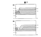
本発明の第2実施例を図7に示す。図7は図5と同様、図1に示した磁気ヘッドのA面、B面の断面を示したものである。
【0029】
第2実施例は下部絶縁層或いは上部絶縁層に低抵抗率絶縁膜を用いる場合である。この場合は使用する材料の絶縁特性と、段差部の付きまわりによる膜厚の減少による絶縁破壊電圧の減少などを考慮に入れて、下部絶縁層或いは上部絶縁層に低抵抗率絶縁膜を用いた方がよい。この方法の利点は第1実施例よりも工程が短縮できる点である。下部絶縁層に低抵抗率絶縁膜を用いた場合について考えると、第1実施例では第2下部絶縁層を形成するため、第1下部絶縁層を所定の形状にしなければならないが、下部絶縁層に低抵抗率絶縁膜を用いれば、第1、第2下部絶縁層を所定の形状に作るための工程が短縮できる。
【0030】
本発明の第3実施例について説明する。
【0031】
低抵抗率絶縁膜を挟むメタル層の面積大きければ、低抵抗率絶縁膜を通って流れる微小電流が多くなるので、静電気などによる絶縁破壊が起こり難い。従って、低抵抗率絶縁膜を挟んでいるシールド層や電極層の面積は広い方がよい。しかし、別の要因でシールド層の面積を小さくしなければならない場合がある。例として上部シールド層の面積を小さくした場合について説明する。
【0032】
図8aは面積を小さくした上部シールド層まで形成した時の状態である(第1実施例の図6fに相当する)。上部シールド層60は別の要因で指定された小さな形状をしている。図の右下には低抵抗率絶縁膜を用いて上部シールド層60と第2電極層42との電位差を低減させる役割を担う端子61が形成されている。更に上部シールド層60と端子61を接続するための配線パターン62が形成されている。端子61及び配線パターン62の材料は特に指定はないが、プロセス上、上部シールド層60と同じ材料であれば、上部シールド層60を形成する工程で一緒にパターニングできるので容易に作製できる。また、第2電極層42が低抵抗率絶縁膜を挟んで端子61と対向するように第2電極層42の形状を工夫する必要がある。例えば図8aのように端子61と対向するように第2電極層42の形状を拡張すればよい。
【0033】
図8a中のC−C‘部分の断面を図8bに示す(但し、基板をスライダにする際、切断される部分は図示していない)。上部シールド層60は僅かな面積しか低抵抗率絶縁膜と接していないが、端子61では広い面積を低抵抗率絶縁膜を挟んで第2電極層42と対向しているので、もし上部シールド層60に静電気などの電荷が蓄積しても端子61から第2上部絶縁層52を通って第2電極層42に微小電流が流れるので上部シールド層60と第2電極層42(及び電気的に接続されている第1電極層41及びMRセンサ30)の電位差は低減され、絶縁破壊が起こり難くなる。上記実施例では上部シールド層60は僅かに低抵抗率絶縁膜と接しているが、端子61の面積が十分大きければ上部シールド層60は低抵抗率絶縁膜と全く接していなくてもよい。
【0034】
【発明の効果】
以上のようにMRセンサと、少なくとも下部シールド層或いは上部シールド層が対向している部分を抵抗率の高い絶縁膜で形成し、対向していない部分を抵抗率の低い絶縁膜で形成することにより、下部シールド層、電極層(或いはMRセンサ)、上部シールド層に過剰な静電荷が溜まっても低抵抗率絶縁膜を通って微小電流が流れ、下部シールド層、電極層(或いはMRセンサ)、上部シールド層の電位差を低減できる。その結果、静電気による絶縁層の破壊を防ぐことができる。また、過剰な静電荷が溜まっていない時、低抵抗率絶縁膜はメタルと比較すると非常に高い抵抗率を有するため、センス電流をシールドに分流することによるノイズの原因となることはない。
【図面の簡単な説明】
【図1】従来の磁気抵抗効果型ヘッド構造の一例を示す図。
【図2】従来の磁気抵抗効果型ヘッドの再生ヘッドを磁気媒体対向面から見た図。
【図3】窒化珪素の抵抗率−電界特性を示す図。
【図4】アルミナの抵抗率−電界特性を示す図。
【図5】本発明の第1実施例の磁気抵抗効果型ヘッド構造の再生ヘッド部分の奥行き方向の断面図。
【図6】本発明の第1実施例の磁気抵抗効果型ヘッド構造の再生ヘッド部分のプロセス図。
【図7】本発明の第2実施例の磁気抵抗効果型ヘッド構造の再生ヘッド部分の奥行き方向の断面図。
【図8】本発明の第3実施例の磁気抵抗効果型ヘッド構造の再生ヘッド部分の上部シールド層を形成した後のパターン図。
【図9】磁気記録装置の概略図。
【符号の説明】
1…記録ヘッド、 2…再生ヘッド、 10…下部シールド層、
20…下部絶縁層、21…第1下部絶縁層、 22…第2下部絶縁層、
30…MRセンサ、40…電極層、 41…第1電極層、
42…第2電極層、50…上部絶縁層、 51…第1上部絶縁層、
52…第2上部絶縁層、60…上部シールド層、61…端子、
62…配線パターン、101…磁気抵抗効果型ヘッド、
102…磁気記録媒体、
103…磁気抵抗効果型ヘッドを駆動させるための手段、
104…磁気記録媒体を駆動させるための手段、
105…記録再生信号処理手段。[0001]
BACKGROUND OF THE INVENTION
The present invention relates to a magnetoresistive head for reading an information signal from a magnetic medium, and more particularly, to a magnetoresistive head having a structure that prevents breakdown of an insulating layer due to static electricity.
[0002]
[Prior art]
In recent years, with the miniaturization and high performance of magnetic storage devices, magnetoresistive heads that use the magnetoresistive effect (hereinafter referred to as MR heads) have been used as heads for reading information signals from magnetic media. Yes. FIG. 1 shows an example of an MR head. The MR head is a combination of a
[0003]
FIG. 2 shows an example of the structure of the read head viewed from the magnetic medium facing surface. The reproducing head is formed between the
[0004]
The lower
[0005]
[Problems to be solved by the invention]
Magnetic storage devices are becoming smaller and higher in performance year by year, and along with this, the gap length GL of the read head for reading information becomes smaller year by year. Along with this, the film thicknesses of the lower
[0006]
When the thicknesses of the
[0007]
Japanese Patent Application Laid-Open Nos. 7-65324 and 7-65330 disclose a method of electrically short-circuiting the shield layer and the electrode layer. Japanese Patent Laid-Open No. 8-221720 discloses a method of connecting a shield layer and an electrode layer with a high resistivity magnetic material. These methods are methods for preventing breakdown of the insulating layer between the MR sensor and the shield layer by causing the MR sensor and the shield layer to have the same potential when static electricity is generated. However, even when operating as a magnetic head in the apparatus, the current is shunted from the electrode layer to the shield layer, resulting in a decrease in output.
[0008]
An object of the present invention is to provide a magnetoresistive head having a structure capable of preventing the insulation layer between the MR sensor and the shield layer from being broken due to the generation of static electricity even when the gap length is narrowed.
[0009]
Furthermore, there is provided a magnetoresistive head having a structure in which a sense current is not diverted from an electrode layer to a shield layer even when the magnetic head of the present invention is incorporated in a magnetic recording apparatus as shown in FIG. 9 and operated. With the goal.
[0010]
[Means for Solving the Problems]
The magnetoresistive head according to the present invention is formed of an insulating film having a lower resistivity than the portion where the MR sensor and the portion where the lower shield layer or the upper shield layer does not face each other.
[0011]
That is, the present invention is characterized in that an MR sensor including a thin film having at least a magnetoresistive effect or a giant magnetoresistive effect between a lower shield layer and an upper shield layer, a bias layer for applying a longitudinal bias magnetic field to the MR sensor, An electrode layer for supplying a detection current to the MR sensor, a lower insulating layer between the MR sensor and the lower shield layer at a portion facing the magnetic medium, and an upper portion between the MR sensor and the upper shield layer It has an insulating layer, has a lower resistivity than the part where the MR sensor or the electrode layer and the part where the lower shield layer and / or the upper shield layer do not face each other, and the total film thickness in the vertical direction The magnetoresistive head is formed of a large insulating layer.
[0012]
The low resistivity insulating film is preferably formed of nitride, oxynitride of aluminum, silicon or a mixture thereof.
[0013]
In the low resistivity insulating film, the resistivity when the applied electric field is 3 MV / cm is preferably less than 1/1000 of the resistivity when the applied electric field is 1 MV / cm.
[0014]
DETAILED DESCRIPTION OF THE INVENTION
FIG. 3 shows resistivity-electric field characteristics of silicon nitride as an example of the low resistivity insulating film. For comparison, FIG. 4 shows the resistivity-electric field characteristics of alumina generally used in the upper insulating layer and the lower insulating layer. Here, the electric field is a value obtained by dividing the applied voltage by the film thickness. In the case of alumina, the change in resistivity is about two to three orders of magnitude even when the electric field is increased. In the case of silicon nitride, the resistivity decreases exponentially as the electric field increases. For example, the resistivity when the electric field is 1 MV / cm and 3 MV / cm is 10E + 15 Ωcm and 10E + 14 Ωcm in the case of alumina, and 10E + 12 Ωcm and 10E + 8 Ωcm in the case of silicon nitride. That is, when the electric field is 1 MV / cm, the resistivity of silicon nitride is three orders of magnitude smaller than that of alumina, but when the electric field is 3 MV / cm, the resistivity of silicon nitride is six orders of magnitude smaller than that of alumina.
[0015]
Materials such as silicon nitride whose resistivity decreases exponentially with increasing electric field include AlN, Si—Al—N, Si—Al—N—O, SiC, and DLC. An oxide insulating material with many oxygen vacancies also shows similar electrical characteristics.
[0016]
By utilizing such a difference in resistivity of the insulating film, a head can be manufactured in which the insulating layer is prevented from being broken by static electricity or the like. In other words, a high-resistivity insulating film such as alumina is used in a place where the film thickness must be reduced while maintaining insulation, and the electrode layer and shield layer or these metal layers are used in places where the film thickness is not strictly defined. A low-resistivity insulating film such as silicon nitride may be used for an insulating layer sandwiched between metal layers electrically connected to each other. For example, when a high potential difference is generated between the shield layer and the electrode layer due to static electricity or the like, silicon nitride under high voltage is several orders of magnitude smaller than alumina (for example, 6 orders of magnitude smaller when the electric field is 3 MV / cm). Leakage current flows through silicon, and the potential difference between the shield layer and the electrode layer can be relaxed. As a result, dielectric breakdown of the insulating layer can be prevented. Also, the larger the area of the metal layer sandwiching silicon nitride, the easier it is for leakage current to flow. The film thickness of the low resistivity insulating film only needs to be a film thickness that does not cause dielectric breakdown.
[0017]
Furthermore, even if the head with this structure is incorporated into the magnetic recording apparatus as it is and operated, silicon nitride has an insulation resistance close to that of alumina in the normal operating range, so that the sense current leaks to the shield layer and causes noise. There is no.
[0018]
A first embodiment of the present invention is shown in FIG. FIG. 5 shows cross sections of the A and B surfaces of the magnetic head shown in FIG.
[0019]
At least a portion where the
[0020]
An example of this head manufacturing method is shown below. FIG. 6 shows the pattern on the substrate in each step.
[0021]
A lower shield layer 10 (Sendust, Fe-Ni, etc.) is formed on a suitable substrate. A first lower insulating
[0022]
Next, a stencil-like resist pattern is formed in order to make the MR sensor 30 a predetermined shape and to remove the excess first lower insulating
[0023]
In order to connect the
[0024]
A stencil-like resist pattern is formed to form the first upper insulating layer 51 at a predetermined location, and a high resistivity insulating film such as Al 2 O 3 or
[0025]
A resist pattern is formed on the first upper insulating layer 51 or a portion that needs to be electrically connected to the
[0026]
The
[0027]
Sections AA ′ and BB ′ in FIG. 6e are shown in FIGS. 6f and 6g (however, when the substrate is used as a slider, the portion to be cut is not shown). By using the above method, at least the portion where the
[0028]
A second embodiment of the present invention is shown in FIG. FIG. 7 shows a cross section of the A and B surfaces of the magnetic head shown in FIG. 1, as in FIG.
[0029]
In the second embodiment, a low resistivity insulating film is used for the lower insulating layer or the upper insulating layer. In this case, a low-resistivity insulating film is used for the lower insulating layer or the upper insulating layer in consideration of the insulation characteristics of the material used and the reduction of the dielectric breakdown voltage due to the decrease in the film thickness due to the stepped portion. Better. The advantage of this method is that the process can be shortened compared to the first embodiment. Considering the case where a low resistivity insulating film is used for the lower insulating layer, in the first embodiment, the second lower insulating layer is formed. Therefore, the first lower insulating layer must have a predetermined shape. If a low resistivity insulating film is used, the process for forming the first and second lower insulating layers into a predetermined shape can be shortened.
[0030]
A third embodiment of the present invention will be described.
[0031]
If the area of the metal layer sandwiching the low-resistivity insulating film is large, the minute current flowing through the low-resistivity insulating film increases, so that dielectric breakdown due to static electricity or the like hardly occurs. Therefore, it is preferable that the shield layer and the electrode layer sandwiching the low resistivity insulating film have a large area. However, there are cases where the area of the shield layer has to be reduced due to another factor. As an example, a case where the area of the upper shield layer is reduced will be described.
[0032]
FIG. 8a shows a state when the upper shield layer having a reduced area is formed (corresponding to FIG. 6f of the first embodiment). The
[0033]
FIG. 8b shows a cross-section of the CC ′ portion in FIG. 8a (however, the portion to be cut when the substrate is used as a slider is not shown). The
[0034]
【The invention's effect】
As described above, by forming a portion where the MR sensor and at least the lower shield layer or the upper shield layer face each other with an insulating film having a high resistivity, and forming a portion not facing each other with an insulating film having a low resistivity. Even if excessive static charge is accumulated in the lower shield layer, electrode layer (or MR sensor), and upper shield layer, a minute current flows through the low resistivity insulating film, and the lower shield layer, electrode layer (or MR sensor), The potential difference of the upper shield layer can be reduced. As a result, it is possible to prevent the insulating layer from being broken by static electricity. Further, when the excessive static charge is not accumulated, the low resistivity insulating film has a very high resistivity as compared with the metal, so that it does not cause noise due to the distribution of the sense current to the shield.
[Brief description of the drawings]
FIG. 1 is a view showing an example of a conventional magnetoresistive head structure.
FIG. 2 is a diagram of a reproducing head of a conventional magnetoresistive head as viewed from a surface facing a magnetic medium.
FIG. 3 is a graph showing resistivity-electric field characteristics of silicon nitride.
FIG. 4 is a graph showing resistivity-electric field characteristics of alumina.
FIG. 5 is a sectional view in the depth direction of the reproducing head portion of the magnetoresistive head structure according to the first embodiment of the invention.
FIG. 6 is a process diagram of the reproducing head portion of the magnetoresistive head structure according to the first embodiment of the invention.
FIG. 7 is a sectional view in the depth direction of a reproducing head portion of a magnetoresistive head structure according to a second embodiment of the invention.
FIG. 8 is a pattern diagram after forming the upper shield layer of the reproducing head portion of the magnetoresistive head structure of the third embodiment of the invention.
FIG. 9 is a schematic diagram of a magnetic recording apparatus.
[Explanation of symbols]
DESCRIPTION OF
20 ... Lower insulating layer, 21 ... First lower insulating layer, 22 ... Second lower insulating layer,
30 ... MR sensor, 40 ... electrode layer, 41 ... first electrode layer,
42 ... second electrode layer, 50 ... upper insulating layer, 51 ... first upper insulating layer,
52 ... Second upper insulating layer, 60 ... Upper shield layer, 61 ... Terminal,
62 ... wiring pattern, 101 ... magnetoresistive head,
102: Magnetic recording medium,
103: Means for driving the magnetoresistive head
104: Means for driving the magnetic recording medium,
105. Recording / reproduction signal processing means.
Claims (4)
前記下部シールドと前記上部シールドとの間であって、前記 MR センサが形成されていない領域に、前記第一の下部絶縁層に接続し、前記第一の下部絶縁層より低い抵抗率を有する第二の下部絶縁層と、前記第一の上部絶縁層に接続し、前記第一の上部絶縁層より低い抵抗率を有する第二の上部絶縁層とをさらに有し、
前記電極層と前記上部シールドとの間に前記第二の上部絶縁層を有し、前記電極層と前記下部シールドとの間に前記第二の下部絶縁層を有し、
前記第二の上部絶縁層及び前記第二の下部絶縁層において、印加電界3MV/cm時の抵抗率が印加電界1MV/cm時の抵抗率の1000分の1以下になる特性を有することを特徴とする磁気抵抗効果型ヘッド。A lower shield, a first lower insulating layer formed on the lower shield, an MR sensor formed on the first lower insulating layer, and a first upper insulating layer formed on the MR sensor When an upper shield formed on the first upper insulating layer, the magnetoresistive head and an electrode layer which is electrically connected to the MR sensor,
A region between the lower shield and the upper shield, where the MR sensor is not formed, is connected to the first lower insulating layer and has a lower resistivity than the first lower insulating layer. A second lower insulating layer, and a second upper insulating layer connected to the first upper insulating layer and having a lower resistivity than the first upper insulating layer,
Having the second upper insulating layer between the electrode layer and the upper shield, and having the second lower insulating layer between the electrode layer and the lower shield;
The second upper insulating layer and the second lower insulating layer have a characteristic that a resistivity when an applied electric field is 3 MV / cm is less than 1/1000 of a resistivity when an applied electric field is 1 MV / cm. A magnetoresistive head.
Priority Applications (3)
| Application Number | Priority Date | Filing Date | Title |
|---|---|---|---|
| JP13675899A JP4221114B2 (en) | 1999-05-18 | 1999-05-18 | Magnetoresistive head |
| US09/383,214 US6219206B1 (en) | 1999-05-18 | 1999-08-26 | Magneto-resistive effect type head |
| US09/819,811 US6404604B2 (en) | 1999-05-18 | 2001-03-29 | Magneto-resistive effect type head |
Applications Claiming Priority (1)
| Application Number | Priority Date | Filing Date | Title |
|---|---|---|---|
| JP13675899A JP4221114B2 (en) | 1999-05-18 | 1999-05-18 | Magnetoresistive head |
Publications (3)
| Publication Number | Publication Date |
|---|---|
| JP2000331315A JP2000331315A (en) | 2000-11-30 |
| JP2000331315A5 JP2000331315A5 (en) | 2006-04-06 |
| JP4221114B2 true JP4221114B2 (en) | 2009-02-12 |
Family
ID=15182826
Family Applications (1)
| Application Number | Title | Priority Date | Filing Date |
|---|---|---|---|
| JP13675899A Expired - Fee Related JP4221114B2 (en) | 1999-05-18 | 1999-05-18 | Magnetoresistive head |
Country Status (2)
| Country | Link |
|---|---|
| US (2) | US6219206B1 (en) |
| JP (1) | JP4221114B2 (en) |
Families Citing this family (24)
| Publication number | Priority date | Publication date | Assignee | Title |
|---|---|---|---|---|
| SG68063A1 (en) * | 1997-07-18 | 1999-10-19 | Hitachi Ltd | Magnetoresistive effect type reproducing head and magnetic disk apparatus equipped with the reproducing head |
| JP3344468B2 (en) * | 1998-12-21 | 2002-11-11 | アルプス電気株式会社 | Thin film magnetic head |
| US6583971B1 (en) * | 1999-03-09 | 2003-06-24 | Sae Magnetics (Hk) Ltd. | Elimination of electric-pop noise in MR/GMR device |
| JP4221114B2 (en) * | 1999-05-18 | 2009-02-12 | 株式会社日立グローバルストレージテクノロジーズ | Magnetoresistive head |
| JP2001006126A (en) * | 1999-06-17 | 2001-01-12 | Nec Corp | Magneto-resistance effect head, magneto-resistance detection system incorporating the same, and magnetic storage system incorporating the same |
| US6667860B1 (en) * | 1999-10-05 | 2003-12-23 | Seagate Technology Llc | Integrated, on-board device and method for the protection of magnetoresistive heads from electrostatic discharge |
| US6415500B1 (en) * | 2000-01-13 | 2002-07-09 | Headway Technologies, Inc. | Method to prevent electrostatic discharge for MR/GMR wafer fabrication |
| JP3511371B2 (en) * | 2000-04-13 | 2004-03-29 | アルプス電気株式会社 | Thin film magnetic head and method of manufacturing the same |
| JP3929676B2 (en) * | 2000-05-26 | 2007-06-13 | アルプス電気株式会社 | Thin film magnetic head and manufacturing method thereof |
| US6773405B2 (en) * | 2000-09-15 | 2004-08-10 | Jacob Fraden | Ear temperature monitor and method of temperature measurement |
| US6741429B1 (en) * | 2000-09-25 | 2004-05-25 | International Business Machines Corporation | Ion beam definition of magnetoresistive field sensors |
| US7292400B2 (en) * | 2001-04-23 | 2007-11-06 | Seagate Technology Llc | Device for limiting current in a sensor |
| JP3918496B2 (en) * | 2001-10-22 | 2007-05-23 | 株式会社日立製作所 | Liquid crystal display device and manufacturing method thereof |
| US6650511B2 (en) * | 2002-02-11 | 2003-11-18 | International Business Machines Corporation | Magnetic head assembly with electrostatic discharge (ESD) shunt/pads seed layer |
| US20030169539A1 (en) * | 2002-03-07 | 2003-09-11 | International Business Machines Corporation | Electrostatic discharge insensilive recording head with a high-resistance gap layer |
| US6870706B1 (en) * | 2002-08-07 | 2005-03-22 | Headway Technologies, Inc. | Method for suppressing tribocharge in the assembly of magnetic heads |
| US7301732B2 (en) * | 2002-08-07 | 2007-11-27 | Headway Technologies, Inc. | GMR head design that suppresses tribocharge during its assembly |
| JP2004110941A (en) * | 2002-09-19 | 2004-04-08 | Hitachi Ltd | Magnetic recording medium and magnetic storage device |
| US7639459B2 (en) * | 2005-01-10 | 2009-12-29 | Hitachi Global Storage Technologies Netherlands B.V. | Three terminal magnetic sensor having an in-stack longitudinal biasing layer structure |
| US8004795B2 (en) * | 2007-12-26 | 2011-08-23 | Hitachi Global Storage Technologies Netherlands B.V. | Magnetic head design having reduced susceptibility to electrostatic discharge from media surfaces |
| US8223462B2 (en) * | 2008-05-30 | 2012-07-17 | Hitachi Global Storage Technologies Netherlands B.V. | Magnetoresistive sensor design for signal noise pickup reduction for use with deep gap electrostatic discharge shunt |
| DE102016105380A1 (en) | 2016-03-22 | 2017-09-28 | Infineon Technologies Ag | Electric screen between magnetoresistive sensor elements |
| US10354679B2 (en) | 2016-12-13 | 2019-07-16 | International Business Machines Corporation | Magnetic recording module having tunnel valve sensors with dissimilar tunnel barrier resistivities |
| US10014014B1 (en) | 2017-06-14 | 2018-07-03 | International Business Machines Corporation | Magnetic recording apparatus having circuits with differing tunnel valve sensors and about the same resistance |
Family Cites Families (17)
| Publication number | Priority date | Publication date | Assignee | Title |
|---|---|---|---|---|
| US4639806A (en) * | 1983-09-09 | 1987-01-27 | Sharp Kabushiki Kaisha | Thin film magnetic head having a magnetized ferromagnetic film on the MR element |
| JPH05205224A (en) * | 1992-01-27 | 1993-08-13 | Hitachi Ltd | Magnetic head |
| US5609948A (en) * | 1992-08-21 | 1997-03-11 | Minnesota Mining And Manufacturing Company | Laminate containing diamond-like carbon and thin-film magnetic head assembly formed thereon |
| JPH06223331A (en) * | 1993-01-26 | 1994-08-12 | Matsushita Electric Ind Co Ltd | Magnetoresistance effect-type thin-film magnetic head |
| JPH06274830A (en) * | 1993-03-25 | 1994-09-30 | Ngk Insulators Ltd | Thin-film magnetic head |
| JP2741837B2 (en) | 1993-08-06 | 1998-04-22 | インターナショナル・ビジネス・マシーンズ・コーポレイション | Thin film magnetoresistive head |
| US5375022A (en) | 1993-08-06 | 1994-12-20 | International Business Machines Corporation | Magnetic disk drive with electrical shorting protection |
| US5644455A (en) * | 1993-12-30 | 1997-07-01 | Seagate Technology, Inc. | Amorphous diamond-like carbon gaps in magnetoresistive heads |
| US5539598A (en) | 1994-12-08 | 1996-07-23 | International Business Machines Corporation | Electrostatic protection for a shielded MR sensor |
| JPH08273126A (en) * | 1995-03-28 | 1996-10-18 | Sony Corp | Magnetoresistance effect type magnetic head |
| US5986857A (en) * | 1997-02-13 | 1999-11-16 | Sanyo Electric Co., Ltd. | Thin film magnetic head including adhesion enhancing interlayers, and upper and lower gap insulative layers having different hydrogen contents and internal stress states |
| JPH10228610A (en) * | 1997-02-13 | 1998-08-25 | Yamaha Corp | Shield type magnetoresistance effect thin film magnetic head |
| JPH10247307A (en) | 1997-03-04 | 1998-09-14 | Fujitsu Ltd | Magnetic head and magnetic storage device |
| JP3157770B2 (en) * | 1997-09-17 | 2001-04-16 | アルプス電気株式会社 | Thin film magnetic head |
| JP3576361B2 (en) * | 1997-09-18 | 2004-10-13 | 富士通株式会社 | Magnetoresistive head and magnetic recording / reproducing device |
| US6188549B1 (en) * | 1997-12-10 | 2001-02-13 | Read-Rite Corporation | Magnetoresistive read/write head with high-performance gap layers |
| JP4221114B2 (en) * | 1999-05-18 | 2009-02-12 | 株式会社日立グローバルストレージテクノロジーズ | Magnetoresistive head |
-
1999
- 1999-05-18 JP JP13675899A patent/JP4221114B2/en not_active Expired - Fee Related
- 1999-08-26 US US09/383,214 patent/US6219206B1/en not_active Expired - Fee Related
-
2001
- 2001-03-29 US US09/819,811 patent/US6404604B2/en not_active Expired - Fee Related
Also Published As
| Publication number | Publication date |
|---|---|
| US6404604B2 (en) | 2002-06-11 |
| US20010009492A1 (en) | 2001-07-26 |
| US6219206B1 (en) | 2001-04-17 |
| JP2000331315A (en) | 2000-11-30 |
Similar Documents
| Publication | Publication Date | Title |
|---|---|---|
| JP4221114B2 (en) | Magnetoresistive head | |
| KR0153311B1 (en) | Magnetoresistive thin-film magnetic head and the method of fabrication | |
| JP2000207714A (en) | Magneto resistance effect type thin film magnetic head and manufacture of the same | |
| US5371643A (en) | Magnetoresistive head structure that prevents under film from undesirable etching | |
| US6392852B1 (en) | Thin-film magnetic head and method of manufacturing same, and magnetoresistive device | |
| KR100278873B1 (en) | Magnetoresistive effect element and manufacturing method | |
| KR100291696B1 (en) | Magnetic head | |
| JP2731506B2 (en) | Magnetoresistive magnetic head and method of manufacturing the same | |
| JP3553393B2 (en) | Method for manufacturing thin-film magnetic head | |
| US6031691A (en) | Magnetoresistance effect magnetic head and manufacturing method therefor | |
| EP0482642B1 (en) | Composite magnetoresistive thin-film magnetic head | |
| JP3677582B2 (en) | Thin film magnetic head | |
| JP2886783B2 (en) | Magnetoresistive thin-film magnetic head and method of manufacturing the same | |
| JPH0916916A (en) | Thin-film magnetic head and its manufacture | |
| JP3521553B2 (en) | Thin film magnetic head | |
| JP2001250205A (en) | Thin film magnetic head and of its manufacturing method | |
| JP2001256617A (en) | Thin-film magnetic head and method of manufacture | |
| JPH04245011A (en) | Magnetic resistance effect type head | |
| KR20030093939A (en) | Magnetoresistance effect film and spin valve reproducing head | |
| US7522386B2 (en) | CPP thin-film magnetic head having auxiliary conductive layer behind element | |
| JPH0540920A (en) | Composite magnetic head and manufacture thereof | |
| JPH0660328A (en) | Thin film magnetic head and its production | |
| JPH1011717A (en) | Magnetoresistive effect head and its production | |
| JP2001034915A (en) | Magnetoresistive effect type head and magnetic recorder /reproducer employing it | |
| JPH08124120A (en) | Production of magneto-resistive head |
Legal Events
| Date | Code | Title | Description |
|---|---|---|---|
| A521 | Request for written amendment filed |
Free format text: JAPANESE INTERMEDIATE CODE: A523 Effective date: 20060113 |
|
| A621 | Written request for application examination |
Free format text: JAPANESE INTERMEDIATE CODE: A621 Effective date: 20060113 |
|
| A521 | Request for written amendment filed |
Free format text: JAPANESE INTERMEDIATE CODE: A523 Effective date: 20060113 |
|
| RD02 | Notification of acceptance of power of attorney |
Free format text: JAPANESE INTERMEDIATE CODE: A7422 Effective date: 20060510 |
|
| RD04 | Notification of resignation of power of attorney |
Free format text: JAPANESE INTERMEDIATE CODE: A7424 Effective date: 20060510 |
|
| A977 | Report on retrieval |
Free format text: JAPANESE INTERMEDIATE CODE: A971007 Effective date: 20070730 |
|
| A131 | Notification of reasons for refusal |
Free format text: JAPANESE INTERMEDIATE CODE: A131 Effective date: 20070807 |
|
| A521 | Request for written amendment filed |
Free format text: JAPANESE INTERMEDIATE CODE: A523 Effective date: 20071002 |
|
| A131 | Notification of reasons for refusal |
Free format text: JAPANESE INTERMEDIATE CODE: A131 Effective date: 20071113 |
|
| A521 | Request for written amendment filed |
Free format text: JAPANESE INTERMEDIATE CODE: A523 Effective date: 20080104 |
|
| A02 | Decision of refusal |
Free format text: JAPANESE INTERMEDIATE CODE: A02 Effective date: 20080708 |
|
| A521 | Request for written amendment filed |
Free format text: JAPANESE INTERMEDIATE CODE: A523 Effective date: 20080825 |
|
| A521 | Request for written amendment filed |
Free format text: JAPANESE INTERMEDIATE CODE: A523 Effective date: 20080806 |
|
| A911 | Transfer to examiner for re-examination before appeal (zenchi) |
Free format text: JAPANESE INTERMEDIATE CODE: A911 Effective date: 20080912 |
|
| TRDD | Decision of grant or rejection written | ||
| A01 | Written decision to grant a patent or to grant a registration (utility model) |
Free format text: JAPANESE INTERMEDIATE CODE: A01 Effective date: 20081111 |
|
| A01 | Written decision to grant a patent or to grant a registration (utility model) |
Free format text: JAPANESE INTERMEDIATE CODE: A01 |
|
| A61 | First payment of annual fees (during grant procedure) |
Free format text: JAPANESE INTERMEDIATE CODE: A61 Effective date: 20081117 |
|
| FPAY | Renewal fee payment (event date is renewal date of database) |
Free format text: PAYMENT UNTIL: 20111121 Year of fee payment: 3 |
|
| R150 | Certificate of patent or registration of utility model |
Free format text: JAPANESE INTERMEDIATE CODE: R150 |
|
| FPAY | Renewal fee payment (event date is renewal date of database) |
Free format text: PAYMENT UNTIL: 20111121 Year of fee payment: 3 |
|
| FPAY | Renewal fee payment (event date is renewal date of database) |
Free format text: PAYMENT UNTIL: 20121121 Year of fee payment: 4 |
|
| S533 | Written request for registration of change of name |
Free format text: JAPANESE INTERMEDIATE CODE: R313533 |
|
| FPAY | Renewal fee payment (event date is renewal date of database) |
Free format text: PAYMENT UNTIL: 20121121 Year of fee payment: 4 |
|
| R350 | Written notification of registration of transfer |
Free format text: JAPANESE INTERMEDIATE CODE: R350 |
|
| FPAY | Renewal fee payment (event date is renewal date of database) |
Free format text: PAYMENT UNTIL: 20121121 Year of fee payment: 4 |
|
| FPAY | Renewal fee payment (event date is renewal date of database) |
Free format text: PAYMENT UNTIL: 20131121 Year of fee payment: 5 |
|
| R250 | Receipt of annual fees |
Free format text: JAPANESE INTERMEDIATE CODE: R250 |
|
| LAPS | Cancellation because of no payment of annual fees |