EP0859331B1 - Kontaktblock für einen Chipkartenleser - Google Patents
Kontaktblock für einen Chipkartenleser Download PDFInfo
- Publication number
- EP0859331B1 EP0859331B1 EP97122238A EP97122238A EP0859331B1 EP 0859331 B1 EP0859331 B1 EP 0859331B1 EP 97122238 A EP97122238 A EP 97122238A EP 97122238 A EP97122238 A EP 97122238A EP 0859331 B1 EP0859331 B1 EP 0859331B1
- Authority
- EP
- European Patent Office
- Prior art keywords
- contact
- contacts
- carrier
- contact block
- switching
- Prior art date
- Legal status (The legal status is an assumption and is not a legal conclusion. Google has not performed a legal analysis and makes no representation as to the accuracy of the status listed.)
- Expired - Lifetime
Links
Images

Classifications
-
- G—PHYSICS
- G06—COMPUTING OR CALCULATING; COUNTING
- G06K—GRAPHICAL DATA READING; PRESENTATION OF DATA; RECORD CARRIERS; HANDLING RECORD CARRIERS
- G06K7/00—Methods or arrangements for sensing record carriers, e.g. for reading patterns
- G06K7/0013—Methods or arrangements for sensing record carriers, e.g. for reading patterns by galvanic contacts, e.g. card connectors for ISO-7816 compliant smart cards or memory cards, e.g. SD card readers
- G06K7/0021—Methods or arrangements for sensing record carriers, e.g. for reading patterns by galvanic contacts, e.g. card connectors for ISO-7816 compliant smart cards or memory cards, e.g. SD card readers for reading/sensing record carriers having surface contacts
Definitions
- the invention relates to a contact block for a Smart card reader.
- the contact block consists of a Contact carrier and contacts arranged therein.
- the Contacts are with a first end for contacting associated conductor tracks one of the contact block associated printed circuit trained and with their second free end over one associated chip card facing surface of the Contact carrier.
- DE 44 18 609 A1 has a chip card reader Limit switch known, the limit switch through a housing, a membrane switch and Switch contact actuator is formed.
- Smart card readers have the task of making contacts on the an associated card arranged electronic chips in contact a specific (end) position of the card in the reader, so a “reading" of the chip's information, but if necessary also entering information in to enable the chip card.
- Chip card readers of the type mentioned are, for example, in stationary card phones, cell phones, ATMs or the like used.
- a contact switch is known from EP 0 316 699 A1, which forms an insertion end contact.
- the contacts are with their contact ends normally against each other, with a Contact arm holds the other under tension.
- At the The card is inserted into the chip card reader Card against the limit switch until the Detach contact arms from each other. Located at that moment the card is in the end position and is activated.
- the contact switch further developed in that the contact elements initially together (i.e. in one piece) from an electrical molded conductive material, then in the desired Assigned and then positioned in a contact holder be before material and thus be electrically separated from each other. Starting from one first one-piece contact switch this is only in the mounting position separately. The result is the contact switch but again in two parts.
- the contact switch - like the other contacts of the contact block - positioned with one end in the contact carrier and otherwise arranged in the contact carrier so that the switch contact with its other end - like the rest Contacts - protrudes beyond the contact block, and on on the same side as the other contacts.
- the first (assembly) will end of the switching contact - similar to the other contacts - with a trace of the associated printed circuit in Brought in contact and the one running between the contact ends Section designed and guided in the contact carrier, that he when contacting the contacts of the chip card and the remaining contacts of the contact block in contact with one Printed circuit board trace is brought.
- the main advantage over the prior art is that the functional position of the smart card through a one-piece contact switch (switching contact) is displayed and can be activated.
- the card can for example pushed on the side of the contacts or from above onto the Contacts.
- the invention relates then a contact block for a chip card reader the features of claim 1.
- all contacts are aligned parallel to each other are.
- all contacts (including the switching contact) at its first end, which is functional the printed circuit traces assigned, can be mounted identically in the contact carrier.
- the first ends of the contacts for example, be bent into a U-shape, the free Leg end rests against the corresponding conductor track.
- the contact switch in the remaining movably guided in the contact carrier to the to be able to perform the desired switching function.
- an embodiment of the invention provides that the Switching contact with the exception of its first end in one groove running perpendicular to the contact carrier surfaces is feasible in the contact carrier. This section of the switch contact can thus be perpendicular to the surfaces of the contact carrier be moved.
- the groove is at least in Area of the middle section of the switch contact continuously between the contact surfaces of the contact carrier educated. This ensures that the middle section of the switch contact over that of the printed one Circuit facing surface of the contact carrier can be routed to a corresponding conductor track there to contact.
- the contact section of the switching contact in the direction of the printed circuit is formed (bulged). Accordingly, the switching contact can be within the Contact carrier be guided that the molded middle Section in the "normal case" immediately before the printed one Circuit facing surface of the contact carrier stands. When a chip card is inserted, it is then countered the free (second) end of the switch contact and pushes this end towards the contact carrier, whereby at the same time the middle contact section over the surface the contact carrier moves and against an associated Conductor track is guided.
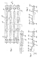
- FIG. 1 With the reference numeral 11 as an insulating body Contact carrier formed from plastic Contact blocks 10 shown.
- this contact carrier 11 eight contacts 12 are arranged here analogously to FIG. 3, and in two rows with four contacts 12 each.
- the contacts 12 have a first end 12.1, which Is bent in a U-shape, in such a way that the free Leg 12u parallel to the underside of the insulating body (Contact carrier) 11 of the contact block 10 runs and over the bottom 10u protrudes (Figure 3).
- FIG. 3 shows - as follows: in one middle section 12.2, the contacts 12 are bulged upwards and protrude above the top 10o of the contact carrier 11.
- the free second end 12.3 is below an as Section 11g of the contact carrier 11 serving as the counter-bearing kept under tension.
- the area is below the counter bearing 11g cut out (area 14) so that the Contacts 12 and in particular their middle section 12.2 in Direction to the bottom 10u of the contact carrier 11 is guided resiliently.
- Figure 1 shows that in addition to the eight contacts 12 mentioned further contact 16 somewhat offset to contacts 12, however parallel to this, is arranged in the contact carrier 11.
- This contact 16 forms a switching contact and its arrangement and function results from Figure 2 as follows:
- a first end 16.1 is analogous to the first end 12.1 Contacts 12 formed and this end will be accordingly the contact ends 12.1 fixed in the contact carrier 11 so that can be referred to the above statements.
- the switching contact runs from this first end 16.1 16 to its opposite free end 16.3 within a groove 18 formed in the contact carrier 11, between the surfaces 10o, 10u of the contact carrier 11 extends.
- the middle section 16.2 of the contact 16 is in the direction molded onto the underside 10u of the contact carrier 11, thus exactly opposite to the middle section 12.2 of the Contacts 12.
- section 16.2 with an associated one (not shown) trace of a printed Circuit 22 contacted which is schematic in Figure 2 is represented by a dashed line.
- Section 16.2 is the same conductor track on which the free leg 16u of the switching contact 16 lies, so that accordingly a short circuit is caused which the End position of the chip card shows and the electrical connection between the contacts of the chip card and the contacts 12 to the corresponding printed conductors Circuit creates on which the contacts 12 with their free Ends 12u.
- the bias of the switch contact 16 causes the Pulling out the card the contact position of the section 16.2 is released again with the conductor track and the switch contact 16 then its shown in Figure 2 "Normal position" (non-functional position) again.
- FIG. 4 shows a further embodiment of a shown contact block according to the invention.
- the contact block 11 is on feet 13 on a circuit board (printed circuit) 22 mounted.
- the respective first ends 12.1, 16.1 of the contacts 12, 16 are L-shaped angled, the free ends on corresponding Conductor tracks of the circuit board 22 are soldered.
- the switch contact 16 extends from the first end 16.1 in substantially parallel to the surfaces 10o, 10u of the Contact carrier 11 through the contact carrier 11 and protrudes with its second end 16.3 in a corresponding recess 19 of the contact carrier 11.
- This end 16.3 of Switch contact 16 is in the longitudinal direction of the switch contact 16 divided, with a first section 16.3.1 S-shaped upwards and a second section 16.3.2 S-shaped is angled downwards.
- the upper section 16.3.1 protrudes again via the top 10o of the contact carrier 11 before (analog to sections 12.2 of contacts 12) and lower section 16.3.2 is shaped so that its free, rounded end at a short distance from the printed circuit board 22 stands when a chip card is not inserted.
Landscapes
- Engineering & Computer Science (AREA)
- Artificial Intelligence (AREA)
- Computer Vision & Pattern Recognition (AREA)
- Physics & Mathematics (AREA)
- General Physics & Mathematics (AREA)
- Theoretical Computer Science (AREA)
- Coupling Device And Connection With Printed Circuit (AREA)
Description
- es entfällt die zweite Kontaktfeder
- der Kontaktblock kann auf diese weise kleiner gestaltet werden, das heißt, es wird Platz auf einer zugehörigen Leiterplatte eingespart
- die Montage des Kontaktblocks wird vereinfacht.
- Das erste Ende, welches in elektrischer Verbindung mit einer Leiterbahn der gedruckten Schaltung steht.
- Das zweite (freie) Ende, welches von der zugeführten Chipkarte beaufschlagt wird und den Schaltkontakt in Richtung auf die gedruckte Schaltung bewegt.
- Einen mittleren Abschnitt, der bei der Bewegung des Schaltkontaktes durch die Chipkarte gegen eine Leiterbahn der gedruckten Schaltung geführt wird und damit eine elektrische Verbindung zum ersten Ende des Schaltkontaktes schafft oder unterbricht, je nachdem, ob der mittlere Abschnitt dieselbe Leiterbahn wie das erste Ende kontaktiert oder eine der Leiterbahn des ersten Endes funktional zugeordnete weitere Leiterbahn.
- Figur 1:
- Eine Aufsicht auf einen erfindungsgemäßen Kontaktblock
- Figur 2:
- einen Vertikalschnitt durch den mit einem Schaltkontakt ausgebildeten Abschnitt des Kontaktblockes nach Figur 1
- Figur 3:
- einen Vertikalschnitt durch den mit einem weiteren Kontakt ausgebildeten Abschnitt des Kontaktblockes nach Figur 1.
- Figur 4:
- einen Vertikalschnitt durch einen Kontaktblock mit einem gegenüber Figur 2 anders gestalteten Schaltkontakt.
Claims (9)
- Kontaktblock (10) für einen Chipkartenleser mit folgenden Merkmalen:1.1 der Kontaktblock (10) besteht aus einem Kontaktträger (11) und darin angeordneten Kontakten (12, 16);1.2 die Kontakte (12, 16) sind mit einem ersten Ende (12.1, 12.16) zur Kontaktierung zugehöriger Leiterbahnen einer dem Kontaktblock (10) zugeordneten gedruckten Schaltung (22) ausgebildet,1.3 die Kontakte (12, 16) stehen mit einem Abschnitt (12.2, 16.3) über die einer zugehörigen Chipkarte zugewandte Oberfläche (10o) des Kontaktträgers (11) vor, gekennzeichnet durch1.4 einen als Schalter dienenden einteiligen Kontakt (16), der im Kontaktträger (11) so geführt ist, daß ein zwischen den Kontaktenden (16.1, 16.3) verlaufender Kontaktabschnitt (16.2) bei der Kontaktierung der Kontakte der Chipkarte mit den übrigen Kontakten (12) des Kontaktblocks (10) selbst und unmittelbar in Kontakt mit einer Leiterbahn der gedruckten Schaltung (22) gebracht wird.
- Kontaktblock nach Anspruch 1, bei dem die Kontakte (12, 16) parallel zueinander ausgerichtet sind.
- Kontaktblock nach Anspruch 1, bei dem das erste Ende (16.1) des Schaltkontaktes (16) U-förmig gebogen ist und der freie U-Schenkel (16u) parallel zum Kontaktträger (11) verlaufend über diesen vorsteht.
- Kontaktblock nach Anspruch 1, bei dem der Schaltkontakt (16) mit Ausnahme seines ersten Endes (16.1) in einer senkrecht zu den Kontaktträger-Oberflächen (10o, 10u) verlaufenden Nut (18) im Kontaktträger (11) führbar ist.
- Kontaktblock nach Anspruch 4, bei dem die Nut (18) zumindest im mittleren Bereich des Schaltkontaktes (16) zwischen den Kontaktträger-Oberflächen (10o, 10u) durchgehend ausgebildet ist.
- Kontaktblock nach Anspruch 1, bei dem der Kontaktabschnitt (16.2) des Schaltkontaktes (16) in Richtung auf die gedruckte Schaltung (22) ausgeformt ist.
- Kontaktblock nach Anspruch 1, bei dem der Kontaktabschnitt (16.2) des Schaltkontaktes (16) derselben Leiterbahn zugeordnet ist wie das erste Ende (16.1) des Schaltkontakts (16).
- Kontaktblock nach Anspruch 1, bei dem die Kontakte (12) zur Verschiebung ihrer mittleren Kontaktabschnitte (12.2) in Richtung auf den Kontaktträger (11) unter Vorspannung im Kontaktträger (11) geführt sind.
- Kontaktblock nach Anspruch 1, bei dem der Schaltkontakt (16) zur Bewegung seines mittleren Kontaktabschnittes (16.2) über die der gedruckten Schaltung (22) zugewandte Oberfläche (10u) hinaus mit seinem freien Ende (16.3) unter Vorspannung gegen ein Gegenlager (20) anliegt.
Applications Claiming Priority (2)
| Application Number | Priority Date | Filing Date | Title |
|---|---|---|---|
| DE19704592 | 1997-02-07 | ||
| DE19704592A DE19704592C2 (de) | 1997-02-07 | 1997-02-07 | Kontaktblock für einen Chipkartenleser |
Publications (2)
| Publication Number | Publication Date |
|---|---|
| EP0859331A1 EP0859331A1 (de) | 1998-08-19 |
| EP0859331B1 true EP0859331B1 (de) | 2001-11-14 |
Family
ID=7819552
Family Applications (1)
| Application Number | Title | Priority Date | Filing Date |
|---|---|---|---|
| EP97122238A Expired - Lifetime EP0859331B1 (de) | 1997-02-07 | 1997-12-17 | Kontaktblock für einen Chipkartenleser |
Country Status (4)
| Country | Link |
|---|---|
| US (1) | US6047890A (de) |
| EP (1) | EP0859331B1 (de) |
| JP (1) | JPH10240892A (de) |
| DE (2) | DE19704592C2 (de) |
Families Citing this family (4)
| Publication number | Priority date | Publication date | Assignee | Title |
|---|---|---|---|---|
| US6412484B1 (en) * | 2000-06-13 | 2002-07-02 | Mallinckrodt Inc. | Fluid control valve for pressure vessel |
| DE502005004005D1 (de) * | 2005-06-23 | 2008-06-19 | Hopt & Schuler Ddm | Kartenleser mit doppel-U-förmig angeordneten Kontaktfedern |
| US8944850B2 (en) * | 2012-10-22 | 2015-02-03 | Apple Inc. | Shielding for edge connector |
| CN105825263B (zh) * | 2016-03-09 | 2018-11-02 | 深圳市文鼎创数据科技有限公司 | 一种pboc智能卡 |
Family Cites Families (7)
| Publication number | Priority date | Publication date | Assignee | Title |
|---|---|---|---|---|
| FR2623314B1 (fr) * | 1987-11-13 | 1991-06-14 | Cit Alcatel | Cadre de contact pour lecteur de carte a puce, avec contact de fin de course |
| DE8817092U1 (de) * | 1988-03-25 | 1992-11-05 | Amphenol Corp., Wallingford, Conn. | Chipkartenleser |
| DE3844783C2 (en) * | 1988-03-25 | 1993-07-15 | Amphenol Corp., Wallingford, Conn., Us | Chip card reader for pay telephone |
| DE4118312C2 (de) * | 1991-06-04 | 1995-03-09 | Amphenol Tuchel Elect | Kontaktsatz für eine Kontaktzonen aufweisende Karte |
| FR2685967B1 (fr) * | 1992-01-07 | 1994-02-25 | Herve Guibert | Etui de protection et de lecture de carte a memoire. |
| DE4418609A1 (de) * | 1994-05-27 | 1995-11-30 | Amphenol Tuchel Elect | Chipkartenleser mit Endlagenschalter und insbesondere den Endlagenschalter an sich |
| DE19521721B4 (de) * | 1995-06-14 | 2006-12-07 | Amphenol-Tuchel Electronics Gmbh | Geschirmte Kontaktiereinrichtung |
-
1997
- 1997-02-07 DE DE19704592A patent/DE19704592C2/de not_active Expired - Fee Related
- 1997-12-17 DE DE59705383T patent/DE59705383D1/de not_active Expired - Fee Related
- 1997-12-17 EP EP97122238A patent/EP0859331B1/de not_active Expired - Lifetime
-
1998
- 1998-01-21 JP JP10042759A patent/JPH10240892A/ja active Pending
- 1998-02-06 US US09/019,716 patent/US6047890A/en not_active Expired - Fee Related
Also Published As
| Publication number | Publication date |
|---|---|
| EP0859331A1 (de) | 1998-08-19 |
| US6047890A (en) | 2000-04-11 |
| DE19704592C2 (de) | 2000-03-16 |
| DE19704592A1 (de) | 1998-08-13 |
| DE59705383D1 (de) | 2001-12-20 |
| JPH10240892A (ja) | 1998-09-11 |
Similar Documents
| Publication | Publication Date | Title |
|---|---|---|
| DE3943703C2 (de) | Chipkartenleser | |
| DE3645268C2 (de) | Kartenaufnehmner für ein Lesegerät für eine Chip-Karte | |
| DE19829551C2 (de) | Kontaktträger | |
| DE112009001374B4 (de) | Kartensockel | |
| DE69811435T2 (de) | Elektrischer Schalter | |
| DE68917080T2 (de) | Elektrischer Verbinder für elektronische Gedächtniskarten, Verfahren der Verwirklichung eines derartigen Verbinders und Lese-Schreibvorrichtung mit diesem Verbinder. | |
| DE1765184C3 (de) | Elektrische Schaltvorrichtung | |
| DE3810275C3 (de) | Chipkartenlesegerät | |
| DE19755715A1 (de) | Chipkartenleser | |
| EP0493522B1 (de) | Chipkartenleser | |
| DE3530221A1 (de) | Miniaturschalter | |
| EP0833268A2 (de) | Kartenlesevorrichtung | |
| EP0859331B1 (de) | Kontaktblock für einen Chipkartenleser | |
| DE4411345C1 (de) | Kontaktschalter | |
| EP0894309B1 (de) | Kartenlesevorrichtung | |
| EP0833271A2 (de) | Kartenlesevorrichtung | |
| DE202008014193U1 (de) | Kontaktblock für einen Chipkartenleser | |
| DE19935188C2 (de) | Kontaktblock für einen Chipkartenleser | |
| DE19521728B4 (de) | Chipkartenleser mit einem Schiebeschalter | |
| DE19616786C2 (de) | Kontaktschalter | |
| DE1223913B (de) | Trennkontaktsatz fuer Trennloetoesenstreifen | |
| DE2612452C3 (de) | Drucktastenschalter | |
| EP0833272A2 (de) | Kartenlesevorrichtung | |
| EP1736910A1 (de) | Kartenleser mit symmetrischer Kontaktfeder | |
| EP1060452A1 (de) | Universalschalter für smart card leser |
Legal Events
| Date | Code | Title | Description |
|---|---|---|---|
| PUAI | Public reference made under article 153(3) epc to a published international application that has entered the european phase |
Free format text: ORIGINAL CODE: 0009012 |
|
| AK | Designated contracting states |
Kind code of ref document: A1 Designated state(s): BE DE FR GB IT NL SE |
|
| AX | Request for extension of the european patent |
Free format text: AL;LT;LV;MK;RO;SI |
|
| 17P | Request for examination filed |
Effective date: 19980903 |
|
| AKX | Designation fees paid |
Free format text: BE DE FR GB IT NL SE |
|
| RBV | Designated contracting states (corrected) |
Designated state(s): BE DE FR GB IT NL SE |
|
| 17Q | First examination report despatched |
Effective date: 20000329 |
|
| GRAG | Despatch of communication of intention to grant |
Free format text: ORIGINAL CODE: EPIDOS AGRA |
|
| GRAG | Despatch of communication of intention to grant |
Free format text: ORIGINAL CODE: EPIDOS AGRA |
|
| GRAH | Despatch of communication of intention to grant a patent |
Free format text: ORIGINAL CODE: EPIDOS IGRA |
|
| GRAH | Despatch of communication of intention to grant a patent |
Free format text: ORIGINAL CODE: EPIDOS IGRA |
|
| GRAA | (expected) grant |
Free format text: ORIGINAL CODE: 0009210 |
|
| AK | Designated contracting states |
Kind code of ref document: B1 Designated state(s): BE DE FR GB IT NL SE |
|
| REF | Corresponds to: |
Ref document number: 59705383 Country of ref document: DE Date of ref document: 20011220 |
|
| REG | Reference to a national code |
Ref country code: GB Ref legal event code: IF02 |
|
| PGFP | Annual fee paid to national office [announced via postgrant information from national office to epo] |
Ref country code: NL Payment date: 20020214 Year of fee payment: 5 |
|
| GBT | Gb: translation of ep patent filed (gb section 77(6)(a)/1977) |
Effective date: 20020124 |
|
| PGFP | Annual fee paid to national office [announced via postgrant information from national office to epo] |
Ref country code: SE Payment date: 20020221 Year of fee payment: 5 |
|
| PLBE | No opposition filed within time limit |
Free format text: ORIGINAL CODE: 0009261 |
|
| STAA | Information on the status of an ep patent application or granted ep patent |
Free format text: STATUS: NO OPPOSITION FILED WITHIN TIME LIMIT |
|
| PGFP | Annual fee paid to national office [announced via postgrant information from national office to epo] |
Ref country code: GB Payment date: 20021104 Year of fee payment: 6 |
|
| 26N | No opposition filed | ||
| PGFP | Annual fee paid to national office [announced via postgrant information from national office to epo] |
Ref country code: FR Payment date: 20021202 Year of fee payment: 6 |
|
| PG25 | Lapsed in a contracting state [announced via postgrant information from national office to epo] |
Ref country code: SE Free format text: LAPSE BECAUSE OF NON-PAYMENT OF DUE FEES Effective date: 20021218 |
|
| PGFP | Annual fee paid to national office [announced via postgrant information from national office to epo] |
Ref country code: BE Payment date: 20030116 Year of fee payment: 6 |
|
| PG25 | Lapsed in a contracting state [announced via postgrant information from national office to epo] |
Ref country code: NL Free format text: LAPSE BECAUSE OF NON-PAYMENT OF DUE FEES Effective date: 20030701 |
|
| EUG | Se: european patent has lapsed | ||
| NLV4 | Nl: lapsed or anulled due to non-payment of the annual fee |
Effective date: 20030701 |
|
| PG25 | Lapsed in a contracting state [announced via postgrant information from national office to epo] |
Ref country code: GB Free format text: LAPSE BECAUSE OF NON-PAYMENT OF DUE FEES Effective date: 20031217 |
|
| PG25 | Lapsed in a contracting state [announced via postgrant information from national office to epo] |
Ref country code: BE Free format text: LAPSE BECAUSE OF NON-PAYMENT OF DUE FEES Effective date: 20031231 |
|
| BERE | Be: lapsed |
Owner name: *AMPHENOL-TUCHEL ELECTRONICS G.M.B.H. Effective date: 20031231 |
|
| GBPC | Gb: european patent ceased through non-payment of renewal fee |
Effective date: 20031217 |
|
| PG25 | Lapsed in a contracting state [announced via postgrant information from national office to epo] |
Ref country code: FR Free format text: LAPSE BECAUSE OF NON-PAYMENT OF DUE FEES Effective date: 20040831 |
|
| REG | Reference to a national code |
Ref country code: FR Ref legal event code: ST |
|
| PG25 | Lapsed in a contracting state [announced via postgrant information from national office to epo] |
Ref country code: IT Free format text: LAPSE BECAUSE OF NON-PAYMENT OF DUE FEES;WARNING: LAPSES OF ITALIAN PATENTS WITH EFFECTIVE DATE BEFORE 2007 MAY HAVE OCCURRED AT ANY TIME BEFORE 2007. THE CORRECT EFFECTIVE DATE MAY BE DIFFERENT FROM THE ONE RECORDED. Effective date: 20051217 |
|
| PGFP | Annual fee paid to national office [announced via postgrant information from national office to epo] |
Ref country code: DE Payment date: 20071228 Year of fee payment: 11 |
|
| PG25 | Lapsed in a contracting state [announced via postgrant information from national office to epo] |
Ref country code: DE Free format text: LAPSE BECAUSE OF NON-PAYMENT OF DUE FEES Effective date: 20090701 |