EP0859239A2 - Verfahren und Vorrichtung zum Korrigieren von Fehlausrichtungen zwischen Testnadeln und -punkten während des elektrischen Testens gedruckter Schaltungen, insbesondere während Mehrfachtests - Google Patents
Verfahren und Vorrichtung zum Korrigieren von Fehlausrichtungen zwischen Testnadeln und -punkten während des elektrischen Testens gedruckter Schaltungen, insbesondere während Mehrfachtests Download PDFInfo
- Publication number
- EP0859239A2 EP0859239A2 EP97119848A EP97119848A EP0859239A2 EP 0859239 A2 EP0859239 A2 EP 0859239A2 EP 97119848 A EP97119848 A EP 97119848A EP 97119848 A EP97119848 A EP 97119848A EP 0859239 A2 EP0859239 A2 EP 0859239A2
- Authority
- EP
- European Patent Office
- Prior art keywords
- test
- printed circuit
- circuit boards
- circuit board
- interface
- Prior art date
- Legal status (The legal status is an assumption and is not a legal conclusion. Google has not performed a legal analysis and makes no representation as to the accuracy of the status listed.)
- Ceased
Links
- 238000012360 testing method Methods 0.000 title claims abstract description 129
- 238000000034 method Methods 0.000 title claims abstract description 19
- 238000012937 correction Methods 0.000 claims abstract description 16
- 239000000463 material Substances 0.000 claims description 3
- 125000006850 spacer group Chemical group 0.000 description 8
- 238000010276 construction Methods 0.000 description 4
- 230000009471 action Effects 0.000 description 3
- 238000005259 measurement Methods 0.000 description 2
- 230000006835 compression Effects 0.000 description 1
- 238000007906 compression Methods 0.000 description 1
- 230000008878 coupling Effects 0.000 description 1
- 238000010168 coupling process Methods 0.000 description 1
- 238000005859 coupling reaction Methods 0.000 description 1
- 230000001419 dependent effect Effects 0.000 description 1
- 230000000694 effects Effects 0.000 description 1
- 238000009434 installation Methods 0.000 description 1
- 239000011810 insulating material Substances 0.000 description 1
- 238000004519 manufacturing process Methods 0.000 description 1
- 238000012986 modification Methods 0.000 description 1
- 230000004048 modification Effects 0.000 description 1
- 210000000056 organ Anatomy 0.000 description 1
- 230000008569 process Effects 0.000 description 1
- 230000009467 reduction Effects 0.000 description 1
- 238000005476 soldering Methods 0.000 description 1
- 239000000126 substance Substances 0.000 description 1
Images

Classifications
-
- G—PHYSICS
- G01—MEASURING; TESTING
- G01R—MEASURING ELECTRIC VARIABLES; MEASURING MAGNETIC VARIABLES
- G01R31/00—Arrangements for testing electric properties; Arrangements for locating electric faults; Arrangements for electrical testing characterised by what is being tested not provided for elsewhere
- G01R31/28—Testing of electronic circuits, e.g. by signal tracer
- G01R31/2801—Testing of printed circuits, backplanes, motherboards, hybrid circuits or carriers for multichip packages [MCP]
- G01R31/2806—Apparatus therefor, e.g. test stations, drivers, analysers, conveyors
- G01R31/2808—Holding, conveying or contacting devices, e.g. test adapters, edge connectors, extender boards
Definitions
- the present invention relates to a method for correcting misalignment between the test needles and test points during electrical testing of printed circuit boards, in particular multiple tests, that is tests on a plurality of printed circuit boards.
- the invention also relates to an actuating device for correction of this misalignment.
- PCB printed circuit board
- the electrical test stage for a printed circuit board therefore comes at the end of the production cycle of the circuit.
- the machines used to carry out this type of test normally operate with a universal contact grid, that is, with a constant pitch (generally 100 mils; 2.54 mm), also known as a needle bed .
- the printed circuit board to be tested has connection points between the different components arranged in a variable manner - and therefore not referable to a constant pitch grid - in order to perform the test an interfacing device (adapter or fixture) is inserted that allows the test points on the printed circuit to be electrically connected to the measuring points of the machine (belonging to the universal grid).
- an interfacing device adapter or fixture
- the circuit board In order to allow a correct electrical connection between the circuit board and the machine, the circuit board must be precisely positioned on the interfacing device.
- the consolidated method for ensuring positioning of the circuit board on the interfacing device is to use pins which, being installed on the interfacing device, engage in suitable mechanical service holes provided on the circuit board itself.
- the single printed circuit boards can be physically separate from each other, or arranged on a single plate or panel of base material, which is subjected to electrical testing before the various circuits provided on it are physically separated from each other.
- Each circuit board being tested can be characterized by an error which can be qualitatively and quantitatively different from those of the other circuit boards under simultaneous testing.
- a possible alternative to this could be to test the various circuit boards individually, removing the plate from the test area each time to reposition it in the correct position, according to the circuit board to be tested.
- An object of the invention is to eliminate this drawback, in so-called multiple tests, avoiding removal of the plate after each single test, to perform possible correction of the positioning error.
- Another object of the invention is to permit such multiple tests on both sides of said circuit boards without removing the plate containing the circuit boards.
- Yet another object of the invention is to provide an extremely reliable device that makes it possible to perform rapid and safe correction of the positioning error of the individual circuit boards in the various stages of the multiple test.
- the device for correction of the misalignment between the test needles and test points during electrical testing of printed circuit boards has the characteristics listed in appended independent claim 8.
- a system of micrometic movement servoactuators which makes it possible to assign desired movements to the circuit board centering pin assembly, installed in an interface, advantageously the lower one, though maintaining the reciprocal distance between the pins unchanged.
- the necessary movements can be assigned to the pin assembly to correct the position of one or more printed circuit boards being tested simultaneously in the same machine cycle, and perform the test solely on that board; the necessary movements are then assigned in succession to correct the position on the interface of the other circuit boards, but always one (or more) at a time, thus performing the test individually on each circuit board.
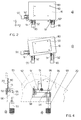
- reference numeral 10 indicates the circuit board being tested, or rather a panel containing a plurality of circuit boards for testing
- 100 indicates the universal measurement point grid of the test machine
- 1 indicates the lower interface device as a whole, interposed between the universal grid 100 and the panel
- 70 indicates a pressure unit of the machine, which provides the necessary force to make the electrical contact between the universal grid and the printed circuit board; in the case of simultaneous testing of both sides of the circuit board, a second interface, or upper interface, is interposed between the pressure unit 70 and the panel 10.
- the interface 1 comprises an upper plate 20, a lower plate 40 and a possible intermediate plate 30, all integral with each other.
- Centering pins 50 for the panel 10 are elastically mounted on the lower plate 40 by means of springs 51.
- the conical end of the pins 50 allows coupling without any play between the pins and the corresponding holes 11 made in the panel 10, whilst the springs 51 compress to allow the panel 10 to rest on the upper plate 20 of the interface 1.
- the centering pins 50 pass in respective holes 21, 31 of the upper plate 20 and of the intermediate plate 30, having a greater diameter than that of the pins, so as to allow a certain radial movement thereof, following the movement of the mobile guide plate 80 of the centering pins 50.
- the mobile plate 80 is operated by micrometric movement servoactuators 90, only one of which is shown in Figure 1.
- test needles 60 which allow the universal grid 100 to be connected to the test points on the surface of the circuit boards undergoing testing, the position of which may not be vertical to a point on the grid 100 of the machine.
- the holes 81 through which the centering pins 50 on the plate 80 pass have the same diameter as the pins and a degree of tolerance H7, whereas the pins have a degree of tolerance H9. This makes it possible for the pins 50 to have a radial play of 0.01 mm in their holes 81, so as to allow axial sliding of the centering pins.
- the thickness of the plate 80 possibly increased locally, makes it possible to limit angular sliding of the pin in its hole.
- the plate 80 is positioned inside the interface 1, immediately below the upper plate 20 thereof.
- the mobility of the plate 80 with respect to the rest of the interface 1 is obtained by making the holes 82 through which the test pins 60 pass and the holes for any internal spacers (see Figure 3) with a radius that is increased with respect to the original one by an amount equal to the maximum desired movement to be imposed on the plate 80.
- the method for correction of the misalignment between the test needles and test points during multiple electrical testing is carried out as follows:
- Figure 2 shows the guide plate 80 for the centering pins 50 of the printed circuit board 10.
- three linear micrometric movement servoactuators 90 are provided, which act on the pivot of a respective radial ball bearing 91, in contrast with a return spring 92 which connects each servoactuator 90 to the plate 80.
- the correct position is that in which the centering pins 50 of the circuit board 10, integral with the plate 80, bring the circuit 10 to take on a position with regard to the interface 1 such that the test points on its surface couple exactly with the test needles that emerge from the upper plate 20 of the interface 1.
- FIG 3 the structure of the lower interface is shown in greater detail than in Figure 1, in that, for example, the distance pieces 4, connecting the lower plate 40 and the upper plate 20, are shown. Also shown is how the lower interface 1 is disposed on the lower universal measuring point grid 100 of the test machine, by means of spring-loaded centering elements 170 that act between this grid 100 and a plate 160 that protects the measurement points and supports the lower interface 1. The protecting and supporting plate 160 is fixed to the lower plate 40 of the interface 1 by means of pins 150.
- a second mobile centering plate operated by actuators 130 is provided in the lower interface 1.
- the mobile plate 110 is disposed beneath the mobile plate 80, between the latter and the intermediate plate 30, and has holes 140 to engage centering pins 50' carried by the upper interface 1', as will be better described below.
- the upper interface 1' comprises a lower plate 20', an upper plate 40' and an intermediate plate 30', corresponding to plates 20, 30 and 40, respectively, of the lower interface 1.
- the lower plate 20' and upper plate 40' are connected to each other by spacers 4'.
- the interface 1' is constrained to a supporting plate 160' by means of reference pins 150'.
- the plate 160' is in turn constrained by means of centering and vertical sliding elements 170' to the upper universal measuring points grid 100' of the test machine, and also serves to protect the measuring points.
- the upper plate 40' of the upper interface 1' is provided with holes 41' coinciding with the inner spacers 4', whose diameter allows said spacers to move radially to the hole.
- the plate 40' is positioned rigidly by means of reference pins 150 on the plate 160', in turn fixed to a grid 100'.
- the remaining components of the interface 1' are constrained rigidly to one another and are mobile with respect to the grid 100' of the machine, thanks to the radial play of the inner spacers 4' in the holes 41' of the plate 40'.
- the spacers end at the top in a washer 42', the flange 43' of which prevents the plate 40' from separating from the interface 1'.
- the thickness of the flange 43' of these washers 42' is smaller than the distance "s" at which the interface is kept by the plate 160'. This allows movement of the spacers 4' (and of the structure of the interface 1' connected to them) without friction forces being generated against the plate 160'.
- the holes 45' for passage of the pins 50' in the upper plate 40' have such a diameter as to allow radial movement of the pins 50' when these move together with the mobile portion of the interface.
- the diameter of the through holes in the remaining plates is the minimum necessary to obtain axial sliding of the pins 50' (typically 0.01 - 0.03 mm).
- the centering action, or movement of the mobile part of the interface 1' is achieved by means of the pins 50' of the upper interface 1' which engage in the holes 140 in the mobile plate 110.
- the pins enter into contact with the plate 110 before the interface 1' has entered into contact with the circuit board 10.
- the pins 50' are returned toward the centre of the holes 140 that are situated in the "correct" position, thus transferring forces to the mobile structure of the interface. These forces cause movement of this mobile structure of the interface 1', that is of the elements situated beneath the upper plate 40'.
- the extent of this movement is to be considered within 0.5 mm.
- the test needles 60' allow this movement thanks to the diameters of the holes in the plates of the interface 1' and to a small extent also thanks to their ability to bend.
- holes 111 with a larger diameter than the pins 50 and with holes 112 with a larger diameter than the spacers 4.
- the mobile plate 80 and the upper plate 20, in alignment with the holes 140 of the mobile plate 110, are provided with respective holes 83, 23 for passage of the centering pins 50' of the upper interface 1'.
- the actuating system shown comprises a micrometric drive head 93.
- the pusher 94 of the head 93 acts on a ball 95 of highly resistant material (for example a ball for ball bearings).
- the ball 95 is inserted by negative tolerance in a recess in a rocker arm 96.
- the rocker arm 96 turns around a pivot 97 and pulls the radial ball bearing 91, integral with it, against the mobile guide plate 80 of the circuit board centering pins 50, not shown in Figure 4.
- the plate 80 is maintained constantly in contact with the bearing 91 by the action of a return spring 92, acting between the mobile plate 80 and a supporting block 98 of the actuator structure, constrained to the structure of the interface 1.
- the ratio between lengths "a” and "b” indicated in Figure 4a represents the reduction ratio that the rocker arm 96 makes it possible to achieve between the movement of the inner pusher 94 of the micrometric head 93 and the actual orthogonal component at the side of the plate 80 of the movement of the bearing 91, that is of the plate itself.
- the ratio "b/a” 5
- the micrometric head has a resolution of 0.01 mm
- the presence of a return spring 92 ensures that any mechanical play is taken up.
- the precision and accuracy of the actual movement of the plate 80 obtained depend largely on the surface finish of the edge of the plate, where the bearing 91 comes to rest.
- the micrometric head 93 is operated manually by an operator to assign the desired movement.
- the linear actuator can be motorized, that is the movement of the head 93, or an organ equivalent to it, can take place in an automated manner, for example with ball bearing microscrews driven by step by step or direct current motors with a closed circuit (negative feedback) control system.
- the system can be automated and controlled with software devices.
Applications Claiming Priority (2)
| Application Number | Priority Date | Filing Date | Title |
|---|---|---|---|
| IT97MI000337A IT1290345B1 (it) | 1997-02-18 | 1997-02-18 | Metodo e dispositivo per la correzione dell'errore di allineamento fra aghi di test e punti di test nella fase di test elettrico di |
| ITMI970337 | 1997-02-18 |
Publications (2)
| Publication Number | Publication Date |
|---|---|
| EP0859239A2 true EP0859239A2 (de) | 1998-08-19 |
| EP0859239A3 EP0859239A3 (de) | 1999-01-20 |
Family
ID=11376053
Family Applications (1)
| Application Number | Title | Priority Date | Filing Date |
|---|---|---|---|
| EP97119848A Ceased EP0859239A3 (de) | 1997-02-18 | 1997-11-13 | Verfahren und Vorrichtung zum Korrigieren von Fehlausrichtungen zwischen Testnadeln und -punkten während des elektrischen Testens gedruckter Schaltungen, insbesondere während Mehrfachtests |
Country Status (4)
| Country | Link |
|---|---|
| US (1) | US6118292A (de) |
| EP (1) | EP0859239A3 (de) |
| CA (1) | CA2221404C (de) |
| IT (1) | IT1290345B1 (de) |
Cited By (11)
| Publication number | Priority date | Publication date | Assignee | Title |
|---|---|---|---|---|
| DE19847146A1 (de) * | 1998-10-13 | 2000-05-04 | Test Plus Electronic Gmbh | Testadapter |
| WO2001040809A1 (de) * | 1999-11-29 | 2001-06-07 | Atg Test Systems Gmbh & Co Kg | Verfahren und vorrichtung zum testen von leiterplatten |
| DE19953602A1 (de) * | 1999-11-08 | 2001-06-21 | Siemens Ag | Vorrichtung zum Prüfen von elektrischen Baugruppen |
| US6353327B2 (en) * | 1997-05-13 | 2002-03-05 | Nidec-Read Corporation | Circuit board misalignment detection apparatus and method |
| EP1231474A2 (de) * | 2001-02-12 | 2002-08-14 | AT & S AUSTRIA TECHNOLOGIE & SYSTEMTECHNIK Aktiengesellschaft | Verfahren und Vorrichtung zum Lokalisieren von möglicherweise fehlerhaften Stiften in einem Prüfadapter sowie Stiftziehwerkzeug |
| WO2003014754A1 (en) * | 2001-08-10 | 2003-02-20 | Mania Entwicklungsgesellschaft Mbh | Apparatus and methods for testing bare circuit boards |
| US6677773B2 (en) | 2000-03-20 | 2004-01-13 | Atg Test Systems Gmbh & Co. Kg | Testing device for printed circuit boards |
| US6727712B2 (en) | 2001-08-10 | 2004-04-27 | James Sabey | Apparatus and methods for testing circuit boards |
| WO2010081834A1 (de) | 2009-01-14 | 2010-07-22 | Dtg International Gmbh | Verfahren zum prüfen von leiterplatten |
| CN104838276A (zh) * | 2012-07-12 | 2015-08-12 | 康拉德有限责任公司 | 制备和/或加工工件的装置 |
| DE102015113046A1 (de) * | 2015-08-07 | 2017-02-09 | Xcerra Corp. | Positioniereinrichtung für einen Paralleltester zum Testen von Leiterplatten und Paralleltester zum Testen von Leiterplatten |
Families Citing this family (10)
| Publication number | Priority date | Publication date | Assignee | Title |
|---|---|---|---|---|
| KR100295228B1 (ko) * | 1998-10-13 | 2001-07-12 | 윤종용 | 통합테스트시스템과그를이용한통합테스트공정수행방법 |
| US6876211B2 (en) * | 2002-03-13 | 2005-04-05 | Seagate Technology Llc | Printed circuit board test fixture that supports a PCB to be tested |
| TW587703U (en) * | 2002-10-18 | 2004-05-11 | Hon Hai Prec Ind Co Ltd | Motherboard test fixture |
| JP2004228332A (ja) * | 2003-01-23 | 2004-08-12 | Yamaha Fine Technologies Co Ltd | 電気検査装置 |
| US7161347B1 (en) * | 2005-07-08 | 2007-01-09 | Credence Systems Corporation | Test head for semiconductor integrated circuit tester |
| US8710858B2 (en) * | 2010-09-23 | 2014-04-29 | Intel Corporation | Micro positioning test socket and methods for active precision alignment and co-planarity feedback |
| CN102680752A (zh) * | 2012-06-04 | 2012-09-19 | 昆山迈致治具科技有限公司 | 柔性线路板电测治具 |
| JP6338085B2 (ja) * | 2014-03-20 | 2018-06-06 | 日本電産リード株式会社 | 可撓性基板検査装置 |
| CN108919088A (zh) * | 2018-04-19 | 2018-11-30 | 深圳市大首自动化技术有限公司 | 一种自动电测机 |
| US11221360B1 (en) | 2020-06-12 | 2022-01-11 | Lat Enterprises, Inc. | Multiple circuit board tester |
Citations (5)
| Publication number | Priority date | Publication date | Assignee | Title |
|---|---|---|---|---|
| JPH0438480A (ja) * | 1990-06-03 | 1992-02-07 | Kyoei Sangyo Kk | プリント配線板検査機用アダプタ上下タイプ |
| GB2285682A (en) * | 1994-01-14 | 1995-07-19 | Gerber Systems Corp | Distortion compensation in pcb optical inspection system |
| DE4406538A1 (de) * | 1994-02-28 | 1995-08-31 | Mania Gmbh | Leiterplatten-Prüfeinrichtung mit Prüfadapter und Verfahren zum Einstellen desselben |
| DE4438316A1 (de) * | 1994-05-20 | 1995-11-23 | Luther & Maelzer Gmbh | System und Verfahren zum Prüfen der korrekten Position einer Kontaktinseln und Leiterbahnen aufweisenden Leiterplatte in einer Prüfvorrichtung |
| EP0831332A1 (de) * | 1996-09-18 | 1998-03-25 | Atg test systems GmbH | Adapter zum Prüfen von elektrischen Leiterplatten |
Family Cites Families (7)
| Publication number | Priority date | Publication date | Assignee | Title |
|---|---|---|---|---|
| US4774462A (en) * | 1984-06-11 | 1988-09-27 | Black Thomas J | Automatic test system |
| US4818933A (en) * | 1986-10-08 | 1989-04-04 | Hewlett-Packard Company | Board fixturing system |
| DE3639361A1 (de) * | 1986-11-18 | 1988-05-19 | Luther Erich | Geraet zum pruefen von leiterplatten |
| US4812754A (en) * | 1987-01-07 | 1989-03-14 | Tracy Theodore A | Circuit board interfacing apparatus |
| US5572144A (en) * | 1993-02-22 | 1996-11-05 | Seagate Technology | Test jig and method for probing a printed circuit board |
| IT1266653B1 (it) * | 1993-11-02 | 1997-01-09 | Circuit Line Spa | Macchina per eseguire il test elettrico simultaneo, sulle due facce di una piastra con circuiti stampati |
| IT1273339B (it) * | 1994-02-24 | 1997-07-08 | Circuit Line Spa | Sistema di marcatura di circuiti stampati |
-
1997
- 1997-02-18 IT IT97MI000337A patent/IT1290345B1/it active IP Right Grant
- 1997-11-13 EP EP97119848A patent/EP0859239A3/de not_active Ceased
- 1997-11-18 CA CA002221404A patent/CA2221404C/en not_active Expired - Fee Related
- 1997-11-25 US US08/977,548 patent/US6118292A/en not_active Expired - Fee Related
Patent Citations (5)
| Publication number | Priority date | Publication date | Assignee | Title |
|---|---|---|---|---|
| JPH0438480A (ja) * | 1990-06-03 | 1992-02-07 | Kyoei Sangyo Kk | プリント配線板検査機用アダプタ上下タイプ |
| GB2285682A (en) * | 1994-01-14 | 1995-07-19 | Gerber Systems Corp | Distortion compensation in pcb optical inspection system |
| DE4406538A1 (de) * | 1994-02-28 | 1995-08-31 | Mania Gmbh | Leiterplatten-Prüfeinrichtung mit Prüfadapter und Verfahren zum Einstellen desselben |
| DE4438316A1 (de) * | 1994-05-20 | 1995-11-23 | Luther & Maelzer Gmbh | System und Verfahren zum Prüfen der korrekten Position einer Kontaktinseln und Leiterbahnen aufweisenden Leiterplatte in einer Prüfvorrichtung |
| EP0831332A1 (de) * | 1996-09-18 | 1998-03-25 | Atg test systems GmbH | Adapter zum Prüfen von elektrischen Leiterplatten |
Non-Patent Citations (1)
| Title |
|---|
| PATENT ABSTRACTS OF JAPAN vol. 016, no. 211 (P-1355), 19 May 1992 -& JP 04 038480 A (KIYOUEI SANGIYOU KK), 7 February 1992 * |
Cited By (17)
| Publication number | Priority date | Publication date | Assignee | Title |
|---|---|---|---|---|
| US6353327B2 (en) * | 1997-05-13 | 2002-03-05 | Nidec-Read Corporation | Circuit board misalignment detection apparatus and method |
| DE19847146A1 (de) * | 1998-10-13 | 2000-05-04 | Test Plus Electronic Gmbh | Testadapter |
| DE19953602A1 (de) * | 1999-11-08 | 2001-06-21 | Siemens Ag | Vorrichtung zum Prüfen von elektrischen Baugruppen |
| DE19953602C2 (de) * | 1999-11-08 | 2002-10-31 | Siemens Ag | Vorrichtung zum Prüfen von elektrischen Baugruppen |
| WO2001040809A1 (de) * | 1999-11-29 | 2001-06-07 | Atg Test Systems Gmbh & Co Kg | Verfahren und vorrichtung zum testen von leiterplatten |
| US6677773B2 (en) | 2000-03-20 | 2004-01-13 | Atg Test Systems Gmbh & Co. Kg | Testing device for printed circuit boards |
| EP1231474A2 (de) * | 2001-02-12 | 2002-08-14 | AT & S AUSTRIA TECHNOLOGIE & SYSTEMTECHNIK Aktiengesellschaft | Verfahren und Vorrichtung zum Lokalisieren von möglicherweise fehlerhaften Stiften in einem Prüfadapter sowie Stiftziehwerkzeug |
| EP1231474A3 (de) * | 2001-02-12 | 2004-08-04 | AT & S AUSTRIA TECHNOLOGIE & SYSTEMTECHNIK Aktiengesellschaft | Verfahren und Vorrichtung zum Lokalisieren von möglicherweise fehlerhaften Stiften in einem Prüfadapter sowie Stiftziehwerkzeug |
| US6727712B2 (en) | 2001-08-10 | 2004-04-27 | James Sabey | Apparatus and methods for testing circuit boards |
| US6734681B2 (en) | 2001-08-10 | 2004-05-11 | James Sabey | Apparatus and methods for testing circuit boards |
| WO2003014754A1 (en) * | 2001-08-10 | 2003-02-20 | Mania Entwicklungsgesellschaft Mbh | Apparatus and methods for testing bare circuit boards |
| WO2010081834A1 (de) | 2009-01-14 | 2010-07-22 | Dtg International Gmbh | Verfahren zum prüfen von leiterplatten |
| DE102009004555A1 (de) | 2009-01-14 | 2010-09-30 | Atg Luther & Maelzer Gmbh | Verfahren zum Prüfen von Leiterplatten |
| KR101337911B1 (ko) * | 2009-01-14 | 2013-12-09 | 디티지 인터나치오날 게엠베하 | 인쇄 회로 기판을 테스트하는 방법 |
| CN104838276A (zh) * | 2012-07-12 | 2015-08-12 | 康拉德有限责任公司 | 制备和/或加工工件的装置 |
| DE102015113046A1 (de) * | 2015-08-07 | 2017-02-09 | Xcerra Corp. | Positioniereinrichtung für einen Paralleltester zum Testen von Leiterplatten und Paralleltester zum Testen von Leiterplatten |
| WO2017025230A1 (de) * | 2015-08-07 | 2017-02-16 | Atg Luther & Maelzer Gmbh | Positioniereinrichtung für einen paralleltester zum testen von leiterplatten und paralleltester zum testen von leiterplatten |
Also Published As
| Publication number | Publication date |
|---|---|
| CA2221404A1 (en) | 1998-08-18 |
| US6118292A (en) | 2000-09-12 |
| ITMI970337A1 (it) | 1998-08-18 |
| EP0859239A3 (de) | 1999-01-20 |
| CA2221404C (en) | 2003-08-05 |
| IT1290345B1 (it) | 1998-10-22 |
Similar Documents
| Publication | Publication Date | Title |
|---|---|---|
| CA2221404C (en) | A method and device for correcting misalignment between test needles and test points during electrical testing of printed circuit boards, particularly during multiple tests | |
| CN1044518C (zh) | 印刷电路板测试夹具与方法 | |
| US6307386B1 (en) | Modular mechanical fixturing and automated handling of printed circuit assemblies on automated test equipment | |
| US4774462A (en) | Automatic test system | |
| US5754057A (en) | Contact mechanism for test head of semiconductor test system | |
| EP1512979A2 (de) | Prüfadapter mit Nadelführung für bestückte Leiterplatten | |
| EP0840130B1 (de) | Hybrid-Prüfadapter für Gebiete mit Standard- und beschränkter Zugänglichkeit | |
| US6429673B1 (en) | Printed wiring board inspection apparatus | |
| US11067601B2 (en) | High accuracy electrical test interconnection device and method for electrical circuit board testing | |
| KR100853766B1 (ko) | 상부 픽스쳐의 미세 수평이동이 가능한 pcb 검사장치 | |
| EP0961127B1 (de) | Verstellbare, schnelle Druckeinrichtung mit einem Schlitten für eine Leiterplatte und modular erweiterbaren Fähigkeiten | |
| US6252414B1 (en) | Method and apparatus for testing circuits having different configurations with a single test fixture | |
| JP2004061264A (ja) | インサーキットテスタ及びプリント基板テスト方法 | |
| KR20220133503A (ko) | 디스플레이 패널 검사장치 | |
| KR100407068B1 (ko) | 인쇄회로 카드 검사방법 | |
| JPH06186271A (ja) | プリント基板検査方法と検査装置 | |
| WO2021182699A1 (ko) | 미세 피치를 갖는 디바이스의 얼라인장치 및 그 방법 | |
| JP3421158B2 (ja) | 配線パターン検査装置 | |
| KR20000015694U (ko) | 인쇄회로기판 검사기구 및 상기 검사기구를 구비한 인쇄회로기 | |
| JPH0814610B2 (ja) | 回路基板検査装置 | |
| JP2000227451A (ja) | 回路基板検査装置 | |
| KR100825861B1 (ko) | 탐침 본딩 방법 | |
| JP2548703Y2 (ja) | 回路基板検査装置 | |
| JPH06160483A (ja) | 基板検査装置 | |
| ITMI960326A1 (it) | Dispositivo di allineamento tra circuito stampato e fixture nella fase di test elettrico di circuiti stampati |
Legal Events
| Date | Code | Title | Description |
|---|---|---|---|
| PUAI | Public reference made under article 153(3) epc to a published international application that has entered the european phase |
Free format text: ORIGINAL CODE: 0009012 |
|
| AK | Designated contracting states |
Kind code of ref document: A2 Designated state(s): BE DE ES FR GB NL SE |
|
| AX | Request for extension of the european patent |
Free format text: AL;LT;LV;MK;RO;SI |
|
| PUAL | Search report despatched |
Free format text: ORIGINAL CODE: 0009013 |
|
| AK | Designated contracting states |
Kind code of ref document: A3 Designated state(s): AT BE CH DE DK ES FI FR GB GR IE IT LI LU MC NL PT SE |
|
| AX | Request for extension of the european patent |
Free format text: AL;LT;LV;MK;RO;SI |
|
| 17P | Request for examination filed |
Effective date: 19990514 |
|
| AKX | Designation fees paid |
Free format text: BE DE ES FR GB NL SE |
|
| RAP1 | Party data changed (applicant data changed or rights of an application transferred) |
Owner name: CIRCUIT LINE S.P.A. |
|
| RAP1 | Party data changed (applicant data changed or rights of an application transferred) |
Owner name: MANIA TECNOLOGIE ITALIA S.P.A. |
|
| 17Q | First examination report despatched |
Effective date: 20010118 |
|
| STAA | Information on the status of an ep patent application or granted ep patent |
Free format text: STATUS: THE APPLICATION HAS BEEN REFUSED |
|
| 18R | Application refused |
Effective date: 20050213 |