EP0849957A2 - Kammfilter und Videogerät damit - Google Patents
Kammfilter und Videogerät damit Download PDFInfo
- Publication number
- EP0849957A2 EP0849957A2 EP97310325A EP97310325A EP0849957A2 EP 0849957 A2 EP0849957 A2 EP 0849957A2 EP 97310325 A EP97310325 A EP 97310325A EP 97310325 A EP97310325 A EP 97310325A EP 0849957 A2 EP0849957 A2 EP 0849957A2
- Authority
- EP
- European Patent Office
- Prior art keywords
- signal
- circuit
- output
- bandpass filter
- delay circuit
- Prior art date
- Legal status (The legal status is an assumption and is not a legal conclusion. Google has not performed a legal analysis and makes no representation as to the accuracy of the status listed.)
- Granted
Links
Images


Classifications
-
- H—ELECTRICITY
- H04—ELECTRIC COMMUNICATION TECHNIQUE
- H04N—PICTORIAL COMMUNICATION, e.g. TELEVISION
- H04N9/00—Details of colour television systems
- H04N9/79—Processing of colour television signals in connection with recording
-
- H—ELECTRICITY
- H04—ELECTRIC COMMUNICATION TECHNIQUE
- H04N—PICTORIAL COMMUNICATION, e.g. TELEVISION
- H04N9/00—Details of colour television systems
- H04N9/77—Circuits for processing the brightness signal and the chrominance signal relative to each other, e.g. adjusting the phase of the brightness signal relative to the colour signal, correcting differential gain or differential phase
- H04N9/78—Circuits for processing the brightness signal and the chrominance signal relative to each other, e.g. adjusting the phase of the brightness signal relative to the colour signal, correcting differential gain or differential phase for separating the brightness signal or the chrominance signal from the colour television signal, e.g. using comb filter
Definitions
- This invention relates to comb filters and to video apparatus, such as color television receivers or video tape recorders (VTRs), that use comb filters.
- VTRs video tape recorders
- a luminance signal and a chrominance signal must be separated from the composite color video signal.
- an input composite color video signal is separated into a luminance signal and a chrominance signal and the luminance signal is frequency modulated and the chrominance signal is frequency converted to the low frequency side of the FM luminance signal for recording.
- a comb filter For a means to separate the luminance signal and the chrominance signal from the composite color video signal as described above, a comb filter has been proposed that uses the correlation of the screen vertical direction of color video signal and the inversion of the phase of chrominance subcarrier every period. This is because separation of the luminance signal and the chrominance signal by use of a band filter such as a bandpass filter mixes a high-frequency component of the luminance signal included in the band of the chrominance signal into the chrominance signal to cause an image degradation known as cross color, whereas use of a comb filter prevents this cross color from occurring.
- a band filter such as a bandpass filter mixes a high-frequency component of the luminance signal included in the band of the chrominance signal into the chrominance signal to cause an image degradation known as cross color
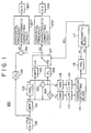
- FIG. 8 is a block diagram illustrating a basic circuit constitution of the comb filter.
- a composite color video signal Sa including a luminance signal Y and a chrominance signal C inputted from an input terminal 11 is supplied to a delay circuit 12 of one horizontal period to be delayed by one horizontal period and the delayed signal is supplied to a first subtracting circuit 13.
- the composite color video signal Sa from the input terminal 11 is also supplied directly to the first subtracting circuit 13.
- the luminance signal component is canceled because of the vertical correlation of the video signal since the luminance the signals in adjacent horizontal intervals are almost the same.
- the phase of the color subcarrier is inverted every horizontal period, so that the color subcarrier components of the adjacent horizontal intervals come in phase in the subtracting circuit 13.
- the chrominance signal component obtained from the subtracting circuit 13 is supplied to a bandpass filter 14 having a pass band of 3.58 MHz ⁇ 500 kHz (in the case of NTSC signal) for example. From this bandpass filter 14, a chrominance signal C is taken to be sent to an output terminal 17C.
- the composite color video signal Sa inputted through the input terminal 11 is supplied to a second subtracting circuit 16 via a delay circuit 15.
- the delay circuit 15 provides a timing match between the composite color video signal Sa and the chrominance signal C outputted from the bandpass filter 14.
- This delay circuit 15 provides a delay obtained by summing the delay of one horizontal period by the first delay circuit 12 and the delay provided by the subtracting circuit 13 and the bandpass filter 14.
- the chrominance signal C obtained by the bandpass filter 14 is supplied to be subtracted from the composite color video signal. Therefore, from the second subtracting circuit 16, a luminance signal Y is obtained to be sent to an output terminal 17Y.
- the luminance signal Y and the chrominance signal C can be separated from the composite color video signal without causing a cross color.
- a comb filter of adaptive type in which the vertical correlation between adjacent three lines is monitored and, between the lines having the vertical correlation, the luminance signal and the chrominance signal separated by the comb filter are used as outputs and, for the lines having no vertical relation, the luminance signal and the chrominance signal separated by the bandpass filter are used as outputs.
- the luminance signal and the chrominance signal separated by the bandpass filter are used as output signals to prevent a dot crawl from occurring.
- two delay circuits for delaying for delaying a composite color video signal for one horizontal period are used to generate a signal delayed behind the current input signal by one horizontal period and a signal delayed behind the current input signal by two horizontal periods to monitor the vertical correlation between the current input signal and the signal delayed by one horizontal period and the vertical correlation between the signal delayed by one horizontal period and the signal delay by two horizontal periods.
- this constitution must have the circuit for monitoring the vertical correlation between the current input signal and the signal delayed by one horizontal period and the circuit for monitoring the vertical correlation between the signal delay by one horizontal period and the signal delayed by two horizontal periods separately, thereby presenting a problem of complicating the circuit constitution.
- a comb filter comprising: a bandpass filter for receiving a composite color video signal, extracting a frequency band component of a chrominance signal from the composite color video signal, and outputting the extracted frequency band component; a first delay circuit for receiving the output of the bandpass filter and delaying the output by one horizontal period; a first subtracting circuit for obtaining a subtracted output between the output signal of the bandpass filter and an output signal of the first delay circuit; an adding circuit for obtaining an added output of the output signal of the bandpass filter and the output of the first delay circuit; a switching circuit for switching between the output of the bandpass filter and the output of the subtracting circuit and outputting the switched output; a correlation detecting circuit for receiving the output of the first subtracting circuit and the output of the adding circuit and, based on a relationship between the two outputs, outputting a binary signal that indicates correlation between the output signal of the bandpass filter and the output signal of the first delay circuit; a second delay circuit for delaying the
- the frequency band component of a chromatic signal is extracted from a composite color video signal by the bandpass filter and the output signal of this bandpass filter is supplied to the first delay circuit to be delayed by one horizontal period. Then, the signal at the input/output terminal of this first delay circuit is subtracted by the first subtracting circuit to provide the chrominance signal from this first subtracting circuit.
- the output signal of this first subtracting circuit is supplied to the correlation detecting circuit and the signal at the input/output signal of the first delay circuit is supplied to the adding circuit.
- the output signal of this adding circuit is also supplied to the correlation detecting circuit.
- the chrominance signal has vertical correlation, the chrominance signal is obtained at a comparatively large level as the output signal of the first subtracting circuit; as the output signal of the adding circuit, a comparatively small level output with the chrominance signal of two horizontal periods canceled is obtained.
- the output signal of the first subtracting circuit is set to a comparatively small level, while the output signal of the adding circuit is set to a comparatively large level.
- the correlation detecting circuit detects the vertical correlation of the chrominance signal between two horizontal scan lines based on the above-mentioned relationship between the output of the first subtracting circuit and the output of the adding circuit and outputs the binary signal of the detection output.
- the binary signal as the detection output of the presence or absence of this vertical correlation is supplied to an arithmetic circuit without change and, at the same time, to the arithmetic circuit via the second delay circuit. From these binary signals of the input/output of the second delay circuit, the arithmetic circuit obtains information about the vertical correlation between the three horizontal scan lines. Then, based on the relationship between the presence and absence of the vertical correlation between the three horizontal scan lines, the arithmetic circuit performs switching operation for switching between the output of the bandpass filter and the output of the first subtracting circuit and outputs the switched output.
- only one delay circuit namely the first delay circuit, my be provided for delaying the signals in the chrominance signal band.
- the second delay circuit for delaying the output of the correlation detecting circuit only delays the binary signal, so that its constitution is simple.
- the only one correlation detecting circuit may be provided for the signal component of the two horizontal scan lines of the input/output of the first delay circuit.
- the preferred form of implementation of the invention provides a comb filter for separating a luminance signal and a chrominance signal from a composite color video signal and outputting the separated signals.
- the preferred form of implementation may enable the provision of an adaptive comb filter that is smaller in circuit scale and simpler in construction than the previously proposed filters.
- a television broadcast signal received at a television antenna 21 is supplied to a tuner 22 and the broadcast signal of a channel selected by the user is converted into a video intermediate frequency signal.
- the resultant video intermediate frequency signal is supplied from the tuner 22 through a video intermediate frequency amplifier 23 to a video detector 24 where a composite color video signal is demodulated.
- this composite color video signal is converted by an A/D converter 25 into a digital signal, which is supplied to an adaptive comb filter 100 to be described later to which the embodied comb filter is applied.
- this digital signal is separated into a digital luminance signal DY and a digital chrominance signal DC.
- the digital outputs DY and DC of this comb filter 100 are supplied to D/A converters 26Y and 26C respectively to be returned to the analog luminance signal Y and the analog chrominance signal C respectively.
- the luminance signal Y is supplied to a matrix circuit 28 without change.
- the chrominance signal C is supplied to a chroma decoder 27 in which color difference signals R-Y and B-Y are decoded. These color difference signals R-Y and B-Y are supplied to the matrix circuit 28.
- the matrix circuit 28 generates primary color signals R, G, and B from the luminance signal Y and the color difference signals R-Y and B-Y and supplies these generated signals R, G, and B to a color cathode ray tube 29 for image reproduction on the screen thereof.
- FIG. 1 shows a circuit constitution of the embodied comb filter while FIG. 2 is a timing chart for describing a circuit operation of this comb filter.
- the composite color video signal is digitized in the A/D converter 25.
- the composite color video signal is a digital signal of which sampling frequency is 4 fs (fs stands for color subcarrier frequency, which is about 3.58 MHz in NTSC) for example, being eight bits per sample.
- This digital composite color video signal is supplied to a bandpass filter 101, in which a frequency band component of the chrominance signal is extracted.
- the output of the bandpass filter 101 is supplied to the first delay circuit 102 and delayed by one horizontal period.
- the delay circuit 102 may be constituted by eight of 910 stages of registers transfered in order by a clock having a frequency of 4 fs.
- the output of the bandpass filter 101 and the output of the first delay circuit 102 are supplied to a first subtracting circuit 103 and an adding circuit 104 respectively. Since the output of the bandpass filter is a chrominance signal band component, the level of output y of the first subtracting circuit 103 and the level of output x of the adding circuit 104 correspond to the vertical correlation between the output of the bandpass filter 101 and the output of the first delay circuit 102.
- the chrominance signal output is obtained as the output of the first subtracting circuit 104 without problem.
- This output of the first subtracting circuit 104 is supplied via a delay circuit 106 to the input terminal B side of a selector switch circuit 107 for taking out a chrominance signal DC to be outputted.
- the delay circuit 106 matches the timing with a signal to be inputted in the input terminal A side of the selector switch circuit 107 and has a delay amount obtained by adding the delay in the first delay circuit 103 to the delay in a bandpass filter 105 to be described later.
- the bandpass filter 105 performs band limitation for eliminating the luminance signal component from the output of the bandpass filter 101 and may be omitted from the circuit constitution.
- the selector switch circuit 107 is operated by a select signal SEL generated depending on presence or absence of vertical correlation as described below.
- the output x of the adding circuit 104 and the output y of the subtracting circuit 103 are supplied to absolute value circuits 111 and 113 respectively in which absolute values of these outputs are obtained.
- the outputs of the absolute value circuits 111 and 113 are supplied to lowpass filters 112 and 114 respectively to provide slowly changing signals
- the correlation arithmetic block 115 executes an evaluating operation based on an evaluating expression shown in Table 1 of FIG. 4 and outputs a binary signal as the evaluation output, or a 1-bit evaluation signal k0.
- the output level of the subtracting circuit 103 is larger enough than the output level of the adding circuit 104 for satisfying
- the output level of the subtracting circuit 103 is small enough than the output level of the adding circuit 104 for satisfying
- the evaluation signal k0 outputted from the correlation detecting block 115 is supplied to an arithmetic block 117 without change.
- the evaluation signal k0 outputted from the correlation detecting block 115 is also supplied to the arithmetic block 117 via the second delay circuit 116 as a signal kl delayed by one horizontal period.
- this second delay circuit 116 may be a delay circuit for delaying the 1-bit evaluation signal k0 by one horizontal period and may be constituted by one of 910 stages of shift registers driven by a clock having a frequency of 4 fs.
- the evaluation signal k0 indicates presence or absence of the vertical correlation in the chrominance signal between the currently inputted scan line and that one horizontal period before.
- the signal k1 indicates presence or absence of the vertical correlation in the chrominance signal between the scan line one horizontal period before and the scan line two horizontal periods before. Namely, the vertical correlation between the three horizontal scan lines can be known by the evaluation signals k0 and k1.
- the arithmetic block 117 receives these evaluation signals k0 and k1, executes an operation that can obtain an operational result shown in Table 2 of FIG. 5, and generates the above-mentioned select signal SEL for the selector switch circuit 107 as the operational result.
- Table 3 of FIG. 6 shows a relationship between this select switch SEL and the switched state of the selector switch circuit 107. To be specific, if the signal SEL is "1," the selector switch circuit 107 is switched to the input terminal A side to select the output of the bandpass filter 105; if the signal SEL is "0," the selector switch circuit 107 is switched to the input terminal B side to select the output of the first subtracting circuit 103.
- the selector switch circuit 107 selects the output of the bandpass filter 105; otherwise, the selector switch circuit 107 selects the output of the first subtracting circuit 103.
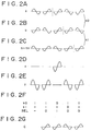
- FIG. 2A shows the phase of the chrominance signal between the horizontal periods in the output a of the bandpass filter 101.
- FIG. 2 shows five horizontal periods. If the chrominance signal has vertical correlation, the phase of the chrominance signal is inverted every horizontal period. In the example of FIG. 2, the phase of the chrominance signal between the second horizontal period and the third horizontal period from the left side is inverted, indicating that there is no vertical correlation.
- FIG. 2B shows a state in which the output is delayed further by one horizontal period (denoted by 1H in the figure).
- the adding circuit 104 addition is performed between the output a and the output b, so that the output x of the adding circuit 104 becomes as shown in FIG. 2 D. If the output a has no correlation with the signal one horizontal period before, the output x becomes a signal of large level.
- the first subtracting circuit 103 subtraction is performed between the output a and the output b, so that the output y of the first subtracting circuit 103 becomes as shown in FIG. 2E. If the output a has no correlation with the signal one horizontal period before, the output y becomes a signal of small level.
- the evaluation signals k0 and k1 obtained as a result of performing the operation of the above-mentioned evaluating expression of FIG. 4 become as shown in FIG. 2F.
- the output SEL obtained as a result of the operation according to the truth table of FIG. 5 performed in the arithmetic block 117 also becomes as shown in FIG. 2F.
- the selector switch circuit 107 selects the output of the bandpass filter 105, so that the proper chrominance signal as shown in FIG. 2G can be always outputted.
- the digital chrominance signal SC obtained from the selector switching circuit 107 is supplied to a second subtracting circuit 109.
- the digital composite color video signal coming from the A/D converter 25 is supplied to this second subtracting circuit 109 via a second delay circuit 108.
- the second delay circuit 108 matches the timing with the output timing of the chrominance signal SC coming from the selector switch circuit 107 and has a delay amount obtained by addition of the delay amount of the bandpass filter 101, the delay amount of the first subtracting circuit 103 and the delay amount of the delay circuit 106.
- the second subtracting circuit 109 subtracts the digital chrominance signal SC from the digital composite color video signal to provide a digital luminance signal SY.
- the digital luminance signal SY coming from the second subtracting circuit 109 is corrected in horizontal frequency characteristic by a horizontal frequency characteristic correcting circuit 120Y.
- the corrected digital luminance signal SY is then supplied to a D/A converter 26Y to be restored to the analog luminance signal Y.
- the digital chrominance signal SC coming from the selector switch circuit 107 is corrected in horizontal frequency characteristic by a horizontal frequency characteristic correcting circuit 120C.
- the corrected digital chrominance signal SC is then supplied to a D/A converter 26C to be restored to the analog chrominance signal C.
- the chrominance signal output can be adaptively obtained according to the vertical correlation between the three horizontal scan lines.
- the delay circuits for one horizontal period may only be the delay circuit 102 for the signal of 8-bit chrominance signal band and the delay circuit 116 for the 1-bit evaluation signal k0. Therefore, a total of nine bits of the delay circuits of one horizontal period may only be provided, thereby decreasing the circuit scale as compared with the ordinary arrangement of the two delay circuits for an 8-bit signal each.
- the circuitry for detecting the presence or absence of vertical correlation may provided only for the input/output of the delay circuit 102. Therefore, the circuit constitution can be simplified and the circuit scale can be reduced as compared with the ordinary constitution having a correlation detecting block for detecting vertical correlation between the currently inputted scan line and the scan line one horizontal period before and another correlation detecting block for detecting vertical correlation between the scan line one horizontal period before and the scan line two horizontal periods before.
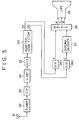
- FIG. 7 is a diagram illustrating a constitution of a VTR to which a comb filter embodying the present invention is applied.
- a composite color video signal inputted through a video input terminal 31 is converted by an A/D converter 32 into a digital composite color video signal to be supplied to an adaptive comb filter 33 constituted by the comb filter 100 having the constitution shown in FIG. 1.
- an adaptive comb filter 33 constituted by the comb filter 100 having the constitution shown in FIG. 1.
- a digital luminance signal DY and a digital chrominance signal DC are separated from the digital composite color video signal.
- the digital luminance signal DY and the digital chrominance signal DC outputted from the adaptive comb filter 33 are restored by a D/A converter 34Y and a D/A converter 34C respectively into the analog luminance signal and the analog chrominance signal C. Then, these luminance signal and the chrominance signal are supplied to a recording processing circuit 35, in which the luminance signal is frequency modulated while the chrominance signal is frequency multiplexed on the low frequency side of the frequency modulated luminance signal.
- the resultant frequency multiplexed signal is supplied to a rotary head 36 to be recorded on magnetic tape.
- the comb filter is a digital circuit and the A/D and D/A converters are externally attached to the comb filter. It will be apparent to those skilled in the art that the comb filter can incorporate these converters.
- the comb filter may have an analog constitution.
- a comb filter for adaptively obtaining chrominance signal output according to the vertical correlation between three horizontal scan lines can be realized with a smaller and simpler circuit constitution than the ordinary constitution.
Landscapes
- Engineering & Computer Science (AREA)
- Multimedia (AREA)
- Signal Processing (AREA)
- Processing Of Color Television Signals (AREA)
Applications Claiming Priority (3)
| Application Number | Priority Date | Filing Date | Title |
|---|---|---|---|
| JP35492496 | 1996-12-21 | ||
| JP354924/96 | 1996-12-21 | ||
| JP35492496A JP3980692B2 (ja) | 1996-12-21 | 1996-12-21 | クシ形フィルタおよび映像機器 |
Publications (3)
| Publication Number | Publication Date |
|---|---|
| EP0849957A2 true EP0849957A2 (de) | 1998-06-24 |
| EP0849957A3 EP0849957A3 (de) | 1999-08-25 |
| EP0849957B1 EP0849957B1 (de) | 2003-08-27 |
Family
ID=18440829
Family Applications (1)
| Application Number | Title | Priority Date | Filing Date |
|---|---|---|---|
| EP97310325A Expired - Lifetime EP0849957B1 (de) | 1996-12-21 | 1997-12-19 | Kammfilter und Videogerät |
Country Status (6)
| Country | Link |
|---|---|
| US (2) | US6950149B1 (de) |
| EP (1) | EP0849957B1 (de) |
| JP (1) | JP3980692B2 (de) |
| KR (1) | KR100519180B1 (de) |
| DE (1) | DE69724393T2 (de) |
| TW (1) | TW364273B (de) |
Cited By (1)
| Publication number | Priority date | Publication date | Assignee | Title |
|---|---|---|---|---|
| WO1999044370A1 (en) * | 1998-02-27 | 1999-09-02 | Matsushita Electric Industrial Co., Ltd. | Luminance signal and chrominance signal separating circuit |
Families Citing this family (6)
| Publication number | Priority date | Publication date | Assignee | Title |
|---|---|---|---|---|
| GB9703143D0 (en) * | 1997-02-14 | 1997-04-02 | Vistek Electronics | An improved method of luminance and chrominance separation for video signals |
| US7227587B2 (en) * | 2003-03-05 | 2007-06-05 | Broadcom Corporation | System and method for three dimensional comb filtering |
| US8553155B2 (en) * | 2003-03-05 | 2013-10-08 | Broadcom Corporation | System and method for three dimensional comb filtering |
| JP3879692B2 (ja) | 2003-04-09 | 2007-02-14 | ソニー株式会社 | 映像信号処理装置及びそれを用いたテレビ受像機 |
| US8306125B2 (en) * | 2006-06-21 | 2012-11-06 | Digital Video Systems, Inc. | 2-bin parallel decoder for advanced video processing |
| WO2015052002A1 (en) * | 2013-10-08 | 2015-04-16 | Koninklijke Philips N.V. | Corrected multiple-slice magnetic resonance imaging |
Family Cites Families (10)
| Publication number | Priority date | Publication date | Assignee | Title |
|---|---|---|---|---|
| JPS5760791A (en) * | 1980-09-30 | 1982-04-12 | Toshiba Corp | Demodulating circuit for wide-band receiving chrominance |
| US5025311A (en) * | 1987-12-28 | 1991-06-18 | Matsushita Electric Industrial Co., Ltd. | Video signal separating apparatus |
| JPH0787594B2 (ja) * | 1988-02-15 | 1995-09-20 | 日本ビクター株式会社 | 相関検出回路 |
| JP2558922B2 (ja) * | 1990-05-15 | 1996-11-27 | 三菱電機株式会社 | Y/c分離装置 |
| JP2674298B2 (ja) * | 1990-10-12 | 1997-11-12 | 日本電気株式会社 | 輝度色分離回路 |
| JPH04252696A (ja) * | 1991-01-29 | 1992-09-08 | Matsushita Electric Ind Co Ltd | 輝度信号色信号分離装置 |
| KR930005626Y1 (ko) * | 1991-02-28 | 1993-08-27 | 김영선 | 탁자다리 결착장치 |
| KR940000414Y1 (ko) * | 1991-04-09 | 1994-01-24 | 주식회사 금성사 | 화상신호의 휘도 신호 및 색신호 분리장치 |
| JP2547686B2 (ja) | 1991-06-21 | 1996-10-23 | 三洋電機株式会社 | 映像信号処理回路 |
| KR100246911B1 (ko) | 1996-01-11 | 2000-03-15 | 윤종용 | 휘도신호와 색호간의 지연차 자동 보상 장치 및 방법 |
-
1996
- 1996-12-21 JP JP35492496A patent/JP3980692B2/ja not_active Expired - Lifetime
-
1997
- 1997-12-16 TW TW086119018A patent/TW364273B/zh active
- 1997-12-19 EP EP97310325A patent/EP0849957B1/de not_active Expired - Lifetime
- 1997-12-19 DE DE69724393T patent/DE69724393T2/de not_active Expired - Fee Related
- 1997-12-22 KR KR1019970071667A patent/KR100519180B1/ko not_active Expired - Fee Related
-
2000
- 2000-11-03 US US09/706,432 patent/US6950149B1/en not_active Expired - Fee Related
-
2001
- 2001-02-13 US US09/782,801 patent/US20010005235A1/en not_active Abandoned
Cited By (2)
| Publication number | Priority date | Publication date | Assignee | Title |
|---|---|---|---|---|
| WO1999044370A1 (en) * | 1998-02-27 | 1999-09-02 | Matsushita Electric Industrial Co., Ltd. | Luminance signal and chrominance signal separating circuit |
| US6188445B1 (en) | 1998-02-27 | 2001-02-13 | Matsushita Electric Industrial Co., Ltd. | Luminance signal and chrominance signal correlation detection and separation circuit |
Also Published As
| Publication number | Publication date |
|---|---|
| JP3980692B2 (ja) | 2007-09-26 |
| EP0849957A3 (de) | 1999-08-25 |
| KR19980064454A (ko) | 1998-10-07 |
| US20010005235A1 (en) | 2001-06-28 |
| EP0849957B1 (de) | 2003-08-27 |
| TW364273B (en) | 1999-07-11 |
| DE69724393T2 (de) | 2004-06-09 |
| KR100519180B1 (ko) | 2005-12-09 |
| DE69724393D1 (de) | 2003-10-02 |
| US6950149B1 (en) | 2005-09-27 |
| JPH10191385A (ja) | 1998-07-21 |
Similar Documents
| Publication | Publication Date | Title |
|---|---|---|
| US5519454A (en) | Luma/chroma separation filter with common delay element for comb filter separation and recursive noise reduction of composite video input signal | |
| EP0546840B1 (de) | Videosignalverarbeitungsvorrichtung | |
| KR100540729B1 (ko) | Y/c 분리 회로 및 y/c 분리 방법 | |
| KR960006081B1 (ko) | 움직임 검출 회로 | |
| US6169583B1 (en) | Method and circuit to determine a noise value that corresponds to the noise in a signal | |
| EP0351787B1 (de) | Schaltung zur Verarbeitung eines Videosignals | |
| US5430500A (en) | Three-dimensional motion detection | |
| EP0849957B1 (de) | Kammfilter und Videogerät | |
| EP0618738B1 (de) | Kammfilter zur Reduzierung von Cross Color-Phänomenen und -Geräuschen | |
| US5225899A (en) | Correlation adaptive luminance and chrominance signal separating circuit | |
| US7515211B2 (en) | Video signal processing circuit, video signal display apparatus, and video signal recording apparatus | |
| US5805238A (en) | Adaptive notch filter for removing residual subcarrier from component video | |
| EP0464879B1 (de) | Vorrichtung zur Trennung des Luminanzsignals und des Chrominanzsignals und Verfahren | |
| JPH0744689B2 (ja) | 動き検出回路 | |
| KR970006790B1 (ko) | 텔레비젼신호처리장치 | |
| US6667776B1 (en) | Video signal processor | |
| KR910007207B1 (ko) | 복합 컬러 비디오신호의 휘도/색도 분리회로 | |
| JP3308705B2 (ja) | インパルスノイズ除去回路 | |
| KR900006475B1 (ko) | 텔레비젼 신호처리회로 | |
| US5303038A (en) | Circuit arrangement for A/D conversion of the color information components of two picture signals | |
| EP1264489B1 (de) | Verfahren und vorrichtung zur verhinderung der datenverfälschung durch videobezogene verbesserungen | |
| JPS63131794A (ja) | 動き検出回路 | |
| JP2609657B2 (ja) | テレビジョン受信機 | |
| JPH05145802A (ja) | インパルスノイズ除去装置 | |
| JPH04188990A (ja) | Yc分離回路 |
Legal Events
| Date | Code | Title | Description |
|---|---|---|---|
| PUAI | Public reference made under article 153(3) epc to a published international application that has entered the european phase |
Free format text: ORIGINAL CODE: 0009012 |
|
| AK | Designated contracting states |
Kind code of ref document: A2 Designated state(s): DE FR GB |
|
| AX | Request for extension of the european patent |
Free format text: AL;LT;LV;MK;RO;SI |
|
| PUAL | Search report despatched |
Free format text: ORIGINAL CODE: 0009013 |
|
| AK | Designated contracting states |
Kind code of ref document: A3 Designated state(s): AT BE CH DE DK ES FI FR GB GR IE IT LI LU MC NL PT SE |
|
| AX | Request for extension of the european patent |
Free format text: AL;LT;LV;MK;RO;SI |
|
| 17P | Request for examination filed |
Effective date: 20000204 |
|
| AKX | Designation fees paid |
Free format text: DE FR GB |
|
| 17Q | First examination report despatched |
Effective date: 20010320 |
|
| GRAH | Despatch of communication of intention to grant a patent |
Free format text: ORIGINAL CODE: EPIDOS IGRA |
|
| GRAS | Grant fee paid |
Free format text: ORIGINAL CODE: EPIDOSNIGR3 |
|
| GRAA | (expected) grant |
Free format text: ORIGINAL CODE: 0009210 |
|
| AK | Designated contracting states |
Designated state(s): DE FR GB |
|
| REG | Reference to a national code |
Ref country code: GB Ref legal event code: FG4D |
|
| REF | Corresponds to: |
Ref document number: 69724393 Country of ref document: DE Date of ref document: 20031002 Kind code of ref document: P |
|
| ET | Fr: translation filed | ||
| PLBE | No opposition filed within time limit |
Free format text: ORIGINAL CODE: 0009261 |
|
| STAA | Information on the status of an ep patent application or granted ep patent |
Free format text: STATUS: NO OPPOSITION FILED WITHIN TIME LIMIT |
|
| 26N | No opposition filed |
Effective date: 20040528 |
|
| PGFP | Annual fee paid to national office [announced via postgrant information from national office to epo] |
Ref country code: FR Payment date: 20041208 Year of fee payment: 8 |
|
| PGFP | Annual fee paid to national office [announced via postgrant information from national office to epo] |
Ref country code: GB Payment date: 20041215 Year of fee payment: 8 |
|
| PGFP | Annual fee paid to national office [announced via postgrant information from national office to epo] |
Ref country code: DE Payment date: 20041216 Year of fee payment: 8 |
|
| PG25 | Lapsed in a contracting state [announced via postgrant information from national office to epo] |
Ref country code: GB Free format text: LAPSE BECAUSE OF NON-PAYMENT OF DUE FEES Effective date: 20051219 |
|
| PG25 | Lapsed in a contracting state [announced via postgrant information from national office to epo] |
Ref country code: DE Free format text: LAPSE BECAUSE OF NON-PAYMENT OF DUE FEES Effective date: 20060701 |
|
| GBPC | Gb: european patent ceased through non-payment of renewal fee |
Effective date: 20051219 |
|
| PG25 | Lapsed in a contracting state [announced via postgrant information from national office to epo] |
Ref country code: FR Free format text: LAPSE BECAUSE OF NON-PAYMENT OF DUE FEES Effective date: 20060831 |
|
| REG | Reference to a national code |
Ref country code: FR Ref legal event code: ST Effective date: 20060831 |