EP0842470B1 - Historische zustandinformation verwendendes entscheidungsprotokoll für zugriff auf ein geteiltes speichergebiet - Google Patents
Historische zustandinformation verwendendes entscheidungsprotokoll für zugriff auf ein geteiltes speichergebiet Download PDFInfo
- Publication number
- EP0842470B1 EP0842470B1 EP96923654A EP96923654A EP0842470B1 EP 0842470 B1 EP0842470 B1 EP 0842470B1 EP 96923654 A EP96923654 A EP 96923654A EP 96923654 A EP96923654 A EP 96923654A EP 0842470 B1 EP0842470 B1 EP 0842470B1
- Authority
- EP
- European Patent Office
- Prior art keywords
- unit
- memory
- processor
- state
- shared memory
- Prior art date
- Legal status (The legal status is an assumption and is not a legal conclusion. Google has not performed a legal analysis and makes no representation as to the accuracy of the status listed.)
- Expired - Lifetime
Links
- 230000015654 memory Effects 0.000 title claims description 240
- 238000000034 method Methods 0.000 claims description 35
- 230000008569 process Effects 0.000 claims description 18
- 230000008859 change Effects 0.000 claims description 7
- 230000004044 response Effects 0.000 claims description 4
- 238000012544 monitoring process Methods 0.000 claims 4
- 238000004891 communication Methods 0.000 description 12
- 230000005540 biological transmission Effects 0.000 description 7
- 238000010586 diagram Methods 0.000 description 6
- 230000000694 effects Effects 0.000 description 5
- 230000008878 coupling Effects 0.000 description 4
- 238000010168 coupling process Methods 0.000 description 4
- 238000005859 coupling reaction Methods 0.000 description 4
- 238000013459 approach Methods 0.000 description 3
- 230000003068 static effect Effects 0.000 description 3
- 238000013500 data storage Methods 0.000 description 2
- 230000006870 function Effects 0.000 description 2
- 238000012986 modification Methods 0.000 description 2
- 230000004048 modification Effects 0.000 description 2
- 238000012545 processing Methods 0.000 description 2
- 230000009471 action Effects 0.000 description 1
- 230000004075 alteration Effects 0.000 description 1
- 230000008901 benefit Effects 0.000 description 1
- 238000004590 computer program Methods 0.000 description 1
- 238000013461 design Methods 0.000 description 1
- 230000007246 mechanism Effects 0.000 description 1
- 230000003287 optical effect Effects 0.000 description 1
- 230000002093 peripheral effect Effects 0.000 description 1
- 230000000704 physical effect Effects 0.000 description 1
- 230000011664 signaling Effects 0.000 description 1
- 239000000126 substance Substances 0.000 description 1
Images


Classifications
-
- G—PHYSICS
- G06—COMPUTING; CALCULATING OR COUNTING
- G06F—ELECTRIC DIGITAL DATA PROCESSING
- G06F9/00—Arrangements for program control, e.g. control units
- G06F9/06—Arrangements for program control, e.g. control units using stored programs, i.e. using an internal store of processing equipment to receive or retain programs
- G06F9/46—Multiprogramming arrangements
- G06F9/52—Program synchronisation; Mutual exclusion, e.g. by means of semaphores
-
- G—PHYSICS
- G06—COMPUTING; CALCULATING OR COUNTING
- G06F—ELECTRIC DIGITAL DATA PROCESSING
- G06F13/00—Interconnection of, or transfer of information or other signals between, memories, input/output devices or central processing units
- G06F13/14—Handling requests for interconnection or transfer
- G06F13/16—Handling requests for interconnection or transfer for access to memory bus
- G06F13/18—Handling requests for interconnection or transfer for access to memory bus based on priority control
Definitions
- the present invention relates to communication between computer systems. More specifically, the present invention relates to an apparatus and method for arbitrating access to a shared memory area.
- a master processor manages the activities of slave processors on shared memory.
- a master processor keeps track of the different areas in memory which are accessed and the purpose for which they are used.
- Each slave processor seeking access to the shared memory must first receive permission from the master processor.
- the master processor arbitrates memory access between slave processors by taking into account the priority of the tasks to be performed and whether the memory is currently being accessed by another processor.
- Another approach for coordinating memory access is self-arbitration of processors through the use of an out-of-band transmission path.
- a separate bus which is not a memory-access bus is used to transmit state information from one processor to another sharing the common memory area. This allows the processors to coordinate memory access among themselves. For example, after a first processor is finished writing data to a location in the shared memory, the first processor can give access to that location of shared memory to a second processor to read that information by signaling the second processor through the out-of-band transmission path. Only the second processor can access the shared memory at that time for that specific purpose.
- Fried discloses a locking circuit for controlling access to locked segments of a shared memory.
- the circuit includes a content-addressable memory (CAM) for storing addresses of the locked memory segments, and for simultaneously comparing a target address (from a requesting process) with the addresses of the locked memory segments and providing a match signal when the target address matches one of the addresses of the locked memory segments.
- CAM content-addressable memory
- a target address is supplied to the CAM. If the target address matches an address in the CAM, then a match signal prevents the control circuit from completing the memory access cycle.
- the requesting ID of the process matches the locking ID (stored in a second memory) of the process that produced the match signal, then the memory access cycle is enabled.
- processors require a large amount of power to operate. This is a problem for computer systems operating under tight power constraints, such as systems operating with batteries. Processors are also relatively large in size compared to other IC components. Thus, depending upon the environment of the computer system, the availability of physical space may not permit the implementation of an additional processor. Perhaps most importantly, the use of an additional processor for the purpose of memory arbitration adds an undesirable cost to the overall computer system.
- Self-arbitration also has its limitations. Computer systems wishing to implement self-arbitration must provide an out-of-band transmission path to allow the processors sharing the memory space to communicate with each other. Design specifications of some computer systems may not permit the implementation of an out-of-band transmission path.
- a memory unit of the present invention comprises a memory cell for storing data.
- An access indication unit is coupled to the memory cell.
- the access indication unit indicates the identity of a first processor accessing the memory cell.
- a state recorder unit is coupled to the access indication unit.
- the state recorder unit records a task pertormed by the first processor.
- a semaphore unit is also coupled to the access indication unit. The semaphore unit reads the access indication unit and prevents a second processor from accessing the memory cell while the first processor is accessing the memory cell.
- An arbitration unit is coupled to the access indication unit. The arbitration unit operates to restrict access of the memory cell to one processor at a time.
- One embodiment of a system for providing communication between a first computer system and a second computer system of the present invention comprises a memory connecting the first computer system to the second computer system.
- the memory stores data transferred between the first computer system and the second computer system.
- An access indication unit is coupled to the memory.
- the access indication unit indicates the identity of a computer system having access to the memory.
- a state recorder unit is coupled to the access indication unit.
- the state recorder unit records a task performed by the processor as a state.
- a first state engine is coupled to the state recorder unit.
- the first state engine instructs the first processor how to process the data in the memory in response to reading a previous task recorded in the state recording unit.
- a second state engine is coupled to the state recorder unit.
- the second state engine instructs the second processor how to process the data in the memory in response to reading the previous task recorded in the state recording unit.
- One embodiment of a method for sending data between a first processor and a second processor comprises the steps of first checking a shared memory space for availability. After checking the shared memory space, identifying a last task performed on the shared memory space. From the last task, determining whether a current task with higher priority must be performed first. Next, transmitting data between the first processor and the shared memory space. After the data are transmitted, recording the present task performed on the shared memory space.
- Figure 1 illustrates in block diagram form a computer system of one embodiment of the present invention.
- the computer system comprises bus 100, keyboard interface 101, external memory 102, mass storage device 103, processor 104 and display device controller 105.
- Bus 100 is coupled to display device controller 105, keyboard interface 101, microprocessor 104, memory 102 and mass storage device 103.
- Display device controller 105 can be coupled to a display device.
- Keyboard interface 101 can be coupled to a keyboard.
- Bus 100 can be a single bus or a combination of multiple buses.
- bus 100 can comprise an Industry Standard Architectural (ISA) bus, an Extended Industry Standard Architecture (EISA) bus, a system bus, a X-bus, PS/2 bus, a Peripheral Components Interconnect (PCI) bus or other buses.
- Bus 100 can also comprise any combination of buses.
- Bus 100 provides communication links between components in the computer system.
- Keyboard interface 101 can be a keyboard controller or other keyboard interface. Keyboard interface 101 can be a dedicated device or can reside in another device such as a bus controller or other controller. Keyboard interface 101 allows coupling of a keyboard to the computer system and transmits signals from a keyboard to the computer system.
- External memory 102 can comprise a dynamic random access memory (DRAM) device, a static random access memory (SRAM) device, or other memory devices.
- External memory 102 stores information and data from mass storage device 103 and processor 104 for use by processor 104.
- Mass storage device 103 can be a hard disk drive, a floppy disk drive, a CD-ROM device, a flash memory device or other mass storage device. Mass storage device 103 provides information and data to external memory 102.
- Processor 104 processes information and data from external memory 102 and stores information and data in external memory 102. Processor 104 also receives signals from keyboard controller 101 and transmits information and data to display device controller 105 for display on a display device. Processor 104 also transmits video images to the display controller for display on a display device.
- Processor 104 can be a complex instruction set computing (CISC) microprocessor, a reduced instruction set computing (RISC) microprocessor, a very long instruction word (VLIW) microprocessor or other processor device.
- Display device controller 105 allows coupling of a display device to the computer system and acts as an interface between the display device and the computer system.
- Display device controller 105 can be a monochrome display adapter (MDA) card, a color graphics adapter (CGA) card, enhanced graphics adapter (EGA) card, multi-color graphics array (MCGA) card, video graphics array (VGA) card, extended graphics array (XGA) card or other display device controller.
- MDA monochrome display adapter
- CGA color graphics adapter
- EGA enhanced graphics adapter
- MCGA multi-color graphics array
- VGA video graphics array
- XGA extended graphics array
- the display device can be a television set, a computer monitor, a flat panel display or other display device.
- the display device receives information and data from processor 104 through display device controller 105 and displays the information and data to the user of the computer system.
- the computer system also comprises shared memory 106.
- Shared memory 106 is coupled to bus 100.
- Shared memory 106 can comprise a dynamic random access memory (DRAM) device, a static random access memory (SRAM) device, or other memory devices.
- Shared memory 106 further comprises memory marking unit 107.
- Memory marking unit 107 operates to record the identity of the microprocessor currently accessing the shared memory 106 and the process that was last performed on the shared memory 106.
- State engine 108 is coupled to bus 108. State engine 108 receives information regarding which process was last performed on the shared memory 106 from memory marking unit 107. State engine 108 uses this information to instruct processor 104 on what should be done with shared memory 106.
- Memory marking unit 107 and state engine 108 allows shared memory 106 to be accessed by multiple processors. These processors may either be processors within the same computer system as shared memory 106 or in entirely autonomous computer systems.
- FIG. 2 illustrates one embodiment of the present invention where shared memory 106 is shared between two processors in the same computer system.
- Shared memory 106 is shared by processor 104 coupled to bus 100 and processor 204 coupled to bus 100.
- Memory marking unit 107 and state engine 108 arbitrates the shared memory 106 between processor 104 and processor 204.
- processor 104 or processor 204 seeks access to the shared memory 106, it first reads the content of the memory marking unit 107. If the shared memory is currently being accessed by the other processor, the processor seeking access will not attempt to access the shared memory 106 concurrently. Instead, it will wait and continue to check the status of the shared memory 106 by periodically reading the contents of memory marking unit 107.
- the processor seeking access changes the contents in memory marking unit 107 to indicate that it currently has access to the shared memory 106. This prevents the other processor from accessing the shared memory 106 while the shared memory 106 is being accessed.
- the processor having access to the shared memory 106 loads information from the memory marking unit 107 regarding the process last performed on shared memory 106 into the state engine 108.
- the state engine 108 uses this information to instruct the processor with access on what it should do with the shared memory 106.
- the process last performed on the shared memory 106 may require that the processor with access to first perform a task with higher priority before it can do anything else with the shared memory 106. In this situation, the state engine 108 instructs the processor having access to perform this high priority task. If, on the other hand, the process last performed on the shared memory 106 does not require the processor seeking access to perform any other task, the processor is allowed to perform any task it wishes. After the processor having access has completed performing its task, it updates the contents in the memory marking unit 107 to reflect the activities that have occurred. This allows the next processor seeking access to the shared memory 106 to know whether there is a task which it must perform.
- the process last performed on shared memory 106 may require that a third processor perform a task having dependency on data currently in shared memory 106 before the processor having access can access the shared memory 106.
- the state engine 108 instructs the process having access to forfeit its access rights and allow the third processor to access the shared memory 106.
- Memory marking unit 107 and state engine 108 allows processors in a multi-processor computer system to communicate with one another without an out-of-band transmission path. This allows arbitration of the shared memory space without the additional hardware cost associated with providing a common connection between the processors in the computer system.
- Memory marking unit 107 and state engine 108 also allows processors in a multi-processor computer system to communicate with one another without a master processor managing the activities in the shared memory space 106. This allows the computer system to operate without consuming additional power, requiring additional space or incurring additional component costs.
- FIG. 3 illustrates an embodiment of the present invention where shared memory 106 is shared between two processors in two autonomous computer systems.
- Shared memory 106 is shared by processor 104 in a first computer system 150 and processor 304 in a second computer system 350.
- Memory marking unit 107 and state engine 108 operate similarly as described in the multi-processor computer system embodiment to coordinate access of the shared memory to processor 104 in the first computer system 150.
- the memory marking unit 107 of the first computer system 150 and state engine 308 located in the second computer system 350 operate to coordinate access of the shared memory 106 to processor 304 in the second computer system.
- processor 104 in the first computer system or the processor 304 in the second computer system 350 seeks access to the shared memory 106, it first reads the content of the memory marking unit 107.
- the processor seeking access will not attempt to access the shared memory 106 concurrently. Instead, it will wait and continue to check the status of the shared memory 106 by periodically reading the contents of memory marking unit 107. If, however, the shared memory 106 is not being accessed by another processor, the processor seeking access changes the contents in memory marking unit 107 to indicate that it currently has access to the shared memory 106. This prevents the other processor from using the shared memory 106 while the shared memory 106 is being accessed.
- the processor having access to the shared memory 106 loads information from the memory marking unit 107 regarding the process last performed on shared memory 106 into a state engine in its computer system.
- the state engine uses this information to instruct the processor having access on what should be done with the shared memory 106.
- the process last performed on the shared memory 106 may require that the processor having access first perform a task with higher priority before it can do anything else with the shared memory 106. In this situation, the state engine instructs the processor having access to perform this high priority task. If on the other hand, the process last performed on the shared memory 106 does not require the processor seeking access to perform any other task, the processor is allowed to perform any task it wishes. After the processor having access has completed performing its task, it updates the contents in the memory marking unit 107 to reflect the activities that have occurred. This allows the next processor seeking access to the shared memory 106 to know whether there is a task which it must perform.
- shared memory 106 is connected across a PCMCIA slot 310 of the second computer system 350.
- the memory marking unit 107 and state engine 108 of the first computer system 150 and the second state engine 308 of the second computer system 350 allow communication between the computer systems to take place through the shared memory space 106.
- the advantage of using a shared memory region simplifies implementation of the system. Other methods of communication between processors (a special bus, through a serial line or network, etc.) require extra hardware, extra software complexity, or both. Additionally, making the data available through a shared memory removes some of the need for each CPU to copy data from some communications channel to its own memory; since the shared space appears as any other RAM, the CPU does not always have to spend time copying to/from the communication channel.
- RPC remote procedure calls
- the RPC interface also allows one computer system to provide system information to the other computer system.
- IPC inter-process communication
- IPC allows information to be sent between two running tasks on two different computer systems.
- Applications of one computer system are permitted to communicate outside the computer system. For example, a key program in one computer system may talk to a doorknob application in a smart door, or a banking program in one computer system may talk to a automated teller machine (ATM) program in an ATM.
- ATM automated teller machine
- Both processors 104 and 304 respond to changes in the marked memory unit 107.
- Processors 104 and 304 can implement a polling routine which periodically checks the status of the memory marking unit 107.
- processors 104 and 304 activate state engines 108 and 308 in their respective computer system. From the information regarding the last task performed on shared memory 106, state engines 108 and 308 instruct the processors on what should be done with the shared memory 106.
- Processors 104 and 304 can also implement circuitry which monitors the status of the memory marking unit 107 and sends an interrupt to the processors 104 and 304 whenever the contents of the memory marking unit 107 is changed.
- the processors 104 and 304 start the state engines 108 and 308 which instruct the processors 104 and 304 of the procedures that should be performed with the shared memory 106.
- a polling routine is implemented for computer systems which have processors operating at speeds which allow polling to be conducted with small or no effect on user response time.
- Circuitry which monitors the memory marking unit 107 and generates interrupts are implemented for computer systems which have processors operating at speeds too slow to be able to effectively poll the contents of the memory marking unit.
- FIG. 4 illustrates a block diagram of an embodiment of the memory marking unit of the present invention.
- Memory marking unit 407 comprises access indication unit 410, state recording unit 411, arbitration unit 412, and semaphore unit 413.
- Access indication unit 410 operates to identify a processor which is currently accessing the shared memory. The contents of access indication unit 410 may be changed by a processor if the shared memory is not currently being accessed or if the processor changing the contents of the access indication unit 410 is the processor currently accessing the shared memory.
- Arbitration unit 412 is coupled to access indication unit 410.
- Arbitration unit 412 provides hardware arbitration so that if more than one processor attempts to change the contents of access indication unit 410 at one time, only one will succeed. When more than one processor attempts to access the shared memory at one time, each of the processors will try to change the contents of the access indication unit 410 so that it indicates that they have access to the shared memory.
- Arbitration unit 412 can be programmed to give one processor priority over another or to use a predetermined physical property to arbitrate which processor has the right to change the contents of access indication unit 410 first.
- Semaphore unit 413 is coupled to access indication unit 410. Semaphore unit 413 reads the contents of access indication unit 410. When access indication unit 410 identifies that a specific processor has access to the shared memory, semaphore unit 413 prevents any other processor from accessing the shared memory.
- State recording unit 411 is coupled to access indication unit 410. State recording unit 411 operates to identify a task previously performed by a processor on the shared memory. The identity of a task is labeled as a state. The states recorded by state recording unit 411 may be changed only by a processor currently accessing the shared memory.
- Figure 5 illustrates one embodiment of an access indication unit and a state recording unit of the present invention.
- State register 500 is a 8 bit register which comprises access indication unit 510 and state recording unit 511.
- State register 500 is located in the first byte of the shared memory. Locating the state register in the shared space is useful in that it allows the software to access the information just as it would access any other value in the computer's memory; some examples of prior art require special CPU instructions or the presence of a separate memory region. For communication between two separate systems, putting the semaphore/state unit in the same memory region allows control information and data to be communicated to share one "communication channel," as opposed to requiring another bus or any other communications path for the control information.
- the first two bits 501 and 502 of state register 500 represents the access indication unit 510.
- bit 501 When a first processor has access to the shared memory, bit 501 is set at one and bit 502 is set at zero. When a second processor has access to the shared memory, bit 501 is set to zero and bit 502 is set to one.
- the last four bits 505, 506, 507, and 508 of state register 500 represent the state recording unit 511.
- State recording unit 511 can record up to sixteen different states. It is appreciated that additional bits can be used for the access identification unit 510 and state recording unit 511 when more than two processors have access to the shared memory or when more than sixteen states exist.
- Figure 6 is a state diagram of a state engine according to one embodiment of the present invention.
- Figure 6 illustrates five states that can be implemented for arbitrating access of a shared memory between two processors.
- Circle 600 represents state 0. From state 0, the state engine may direct either processor to write to the shared memory.
- Circle 601 represents state 1.
- a first processor writes data into the shared memory. From state 1, the state engine directs the second processor to read the data that was previously written into the shared memory.
- Circle 602 represents state 2.
- the second processor is ready to read the data in shared memory. From state 2, the state engine returns to state 0.
- Circle 603 represents state 3.
- a second processor writes data into the shared memory. From state 3, the state engine directs the first processor to read the data that was previously written into the shared memory.
- Circle 604 represents state 4. At state 4, the first processor is ready to read the data in shared memory. From state 4, the state engine returns to state 0.
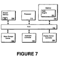
- Figure 7 illustrates in block diagram form a software implementation of the state engine of the present invention.
- the computer system comprises bus 700, microprocessor 710, memory 720, data storage device 730, keyboard controller 740, and display device controller 750.
- Microprocessor 710 can be a complex instruction set computing (CISC) microprocessor, a reduced instruction set computing (RISC) microprocessor or other processor device. Microprocessor 710 executes instructions or code stored in memory 720 and performs operations on data stored in memory 720.
- the computer system further comprises a data storage device 730 such as a hard, floppy, or optical disk drive which is coupled to bus 700.
- Display device controller 750 is also coupled to bus 700. Display device controller 750 allows coupling of a display device to the computer system.
- Keyboard controller 740 allows coupling of a keyboard to the computer system and transmits signals from a keyboard to the computer system.
- Shared memory 706 and memory marking unit 707 function similarly to that of shared memory 106 and memory marking unit 107 as described in Figure 1.
- Memory 720 is coupled to the microprocessor 710 through bus 700.
- Memory 720 can be a dynamic random access memory (DRAM), static random access memory (SRAM) or other memory device.
- Memory 720 can store instruction or code executable by processor 710 that are part of application programs, operating system programs or other computer programs.
- Memory 720 comprises state engine 721.
- State engine 721 comprises a plurality of processor executable instructions that are executed by processor 710 in the manner shown in Figure 8. State engine 721 performs functions similar to that of state engine 108 in Figure 1.
- Figure 8 is a flow chart illustrating a method for arbitrating access to a shared memory according to one embodiment of the present invention.
- the memory marking unit can be a state register for example.
- the memory marking unit contains information regarding whether a processor is currently accessing the state machine and identifies a last task performed on the shared memory.
- a second processor seeking access must wait until the first processor is finished. If the shared memory is not being accessed by another processor, go to block 803.
- Block 803 instructs the routine to change the content of the memory marking unit so that it indicates that the shared memory is currently being accessed by a processor.
- determine whether a task with high priority must be performed This can be achieved by sending the information regarding the identity of the last task performed on the shared memory to a state engine.
- the state engine can contain a state table defining tasks that need to be performed based on a prior task. This is shown in block 804. If a task with high priority exists, go to block 805. If a task with high priority does not exist, go to block 807. If a task with high priority must be performed, instruct the processor which needs to perform the task to perform the task. This is shown in block 805. After the task is performed, record the task in the memory marking unit as shown in block 806.
Landscapes
- Engineering & Computer Science (AREA)
- Theoretical Computer Science (AREA)
- Software Systems (AREA)
- Physics & Mathematics (AREA)
- General Engineering & Computer Science (AREA)
- General Physics & Mathematics (AREA)
- Multi Processors (AREA)
Claims (12)
- Eine Speichereinheit (107, 407) in einem gemeinsamen Speicher (106), die Speichereinheit (107, 407) enthaltend:dadurch gekennzeichnet, daß die Speichereinheit ferner enthält:eine datenspeichernde Speicherzelle;eine mit der Speicherzelle gekoppelte Zugriffsanzeigeeinheit (410), welche eine Identität eines auf die Speicherzelle zugreifenden ersten Prozessors (104) aufzeichnet;eine mit der Zugriffsanzeigeeinheit (410) gekoppelte Semaphoreinheit (413), welche einen Zugriff eines zweiten Prozessors (204, 304) auf die Speicherzelle verhindert, während die Identität des ersten Prozessors (104) in der Zugriffsanzeigeeinheit (410) aufgezeichnet wird;eine mit der Zugriffsanzeigeeinheit (410) gekoppelte Zustandsaufzeichnungseinheit (411), welche die vom ersten Prozessor (104) beschriebene Zustandsinformation aufzeichnet, die von einer Zustandsmaschine (108, 308) gelesen wird, um eine zuvor auf der Speicherzelle ausgeführte Task und die nächsten Tasks zu bestimmen, die auf der Speicherzelle ausgeführt werden können.
- Die Speichereinheit nach Anspruch 1, ferner enthaltend eine mit der Zugriffsanzeigeeinheit (410) gekoppelte Arbitereinheit (412), welche einem Prozessor zu einem Zeitpunkt Zugriff auf einen Prozessor (104, 204, 304) gewährt.
- Die Speichereinheit nach Anspruch 1, wobei die Zugriffsanzeigeeinheit (410) ein Register aufweist.
- Die Speichereinheit nach Anspruch 1, wobei die Zugriffsaufzeichnungseinheit (411) ein Register enthält.
- Ein Computersystem mit einem Bus (100), einem mit dem Bus gekoppelten ersten Prozessor (104) und einem zweiten Prozessor (204, 304), wobei das Computersystem aufweist:dadurch gekennzeichnet, daß das Computersystem ferner enthält:eine gemeinsame Speichereinheit (106) mit einer datenspeichernden Speicherzelle, eine mit der Speicherzelle gekoppelte Zugriffsanzeigeeinheit (410), die eine Identität des auf die Speicherzelle zugreifenden ersten Prozessor (104) aufzeichnet, eine mit der Zugriffsanzeigeeinheit (410) gekoppelte Semaphoreinheit (413), welche einen Zugriff des zweiten Prozessors (204, 304) auf die Speicherzelle verhindert, während die Identität des ersten Prozessor (104) in der Zugriffsanzeigeeinheit (410) aufgezeichnet wird;eine erste Zustandsmaschine (108);und daß die Speichereinheit (106) ferner enthält:eine mit der Zugriffsanzeigeeinheit (410) gekoppelte Zustandsaufzeichnungseinheit (411), die von dem ersten Prozessor (104) geschriebene Zustandsinformationen aufzeichnet, welche von der Zustandsmaschine (108) gelesen wird, um eine zuvor auf der Speicherzelle ausgeführte Task und nächste auf der Speicherzelle auszuführende Tasks zu bestimmen.
- Das Computersystem nach Anspruch 5, ferner enthaltend:eine zweite Zustandsmaschine (308), welche den zweiten Prozessor (304) anweist, wie Daten in der Speicherzelle in Abhängigkeit von der in der Zustandsaufzeichnungseinheit (411) aufgezeichneten Zustandsinformationen zu verarbeiten sind.
- Das Computersystem nach Anspruch 5, ferner eine mit der Zustandsaufzeichnungseinheit (411) gekoppelte Überwachungseinheit enthaltend, wobei die Überwachungseinheit die Zustandsinformationen überwacht und ein Interrupt-Signal an den ersten Prozessor (104) sendet, welcher die erste Zustandsmaschine (108) startet, wenn es eine Änderung in der Zustandsinformation gibt.
- Das Computersystem nach Anspruch 5, ferner eine mit der Zustandsaufzeichnungseinheit (411) gekoppelte Abfrageeinheit enthaltend, die die Zustandsaufzeichnungseinheit (411) nach einer vorgegebenen Zeitspanne überwacht und die erste Zustandsmaschine (108) startet, wenn die Abfrageeinheit eine Änderung der Zustandsinformation feststellt.
- Verfahren zur Zugriffsentscheidung auf einen gemeinsamen Speicher (106) unter einer Vielzahl von Prozessoren (104, 204, 304), das Verfahren gekennzeichnet durch
Bestimmen, ob gerade auf den gemeinsamen Speicher (106) zugegriffen wird;
Identifizieren eines Zustandes des gemeinsamen Speichers (106);
Bestimmen von auf den gemeinsamen Speicher (106) auszuführenden nächsten Tasks aus dem Zustand des gemeinsamen Speichers (106); und
Gewähren von Zugriff auf den gemeinsamen Speicher (106) für einen Prozessor (104, 204, 304) der zum Durchführen einer der nächsten Tasks bezeichnet ist. - Das Verfahren nach Anspruch 9, wobei das Bestimmen, ob auf den gemeinsame Speicher (106) zugegriffen wird, durch Lesen des Inhalts einer Semaphoreinheit (413) erreicht wird.
- Das Verfahren nach Anspruch 9, wobei das Identifizieren des Zustands des gemeinsamen Speichers (106) durch Lesen von Zustandsinformationen in einer Zustandsaufzeichnungseinheit (411) erreicht wird.
- Das Verfahren nach Anspruch 9, wobei das Bestimmen der auf dem gemeinsamen Speicher (106) auszuführenden nächsten Tasks durch Prüfen eines nächsten Zustands in einer Zustandsmaschine erfolgt.
Applications Claiming Priority (3)
| Application Number | Priority Date | Filing Date | Title |
|---|---|---|---|
| US50796295A | 1995-07-27 | 1995-07-27 | |
| US507962 | 1995-07-27 | ||
| PCT/US1996/011306 WO1997005550A1 (en) | 1995-07-27 | 1996-07-02 | Protocol for arbitrating access to a shared memory area using historical state information |
Publications (3)
| Publication Number | Publication Date |
|---|---|
| EP0842470A1 EP0842470A1 (de) | 1998-05-20 |
| EP0842470A4 EP0842470A4 (de) | 2002-01-02 |
| EP0842470B1 true EP0842470B1 (de) | 2003-09-24 |
Family
ID=24020812
Family Applications (1)
| Application Number | Title | Priority Date | Filing Date |
|---|---|---|---|
| EP96923654A Expired - Lifetime EP0842470B1 (de) | 1995-07-27 | 1996-07-02 | Historische zustandinformation verwendendes entscheidungsprotokoll für zugriff auf ein geteiltes speichergebiet |
Country Status (5)
| Country | Link |
|---|---|
| US (1) | US6243793B1 (de) |
| EP (1) | EP0842470B1 (de) |
| AU (1) | AU6452396A (de) |
| DE (1) | DE69630126T2 (de) |
| WO (1) | WO1997005550A1 (de) |
Families Citing this family (36)
| Publication number | Priority date | Publication date | Assignee | Title |
|---|---|---|---|---|
| GB9724028D0 (en) * | 1997-11-13 | 1998-01-14 | Advanced Telecommunications Mo | Shared memory access controller |
| US6996656B2 (en) * | 2002-10-31 | 2006-02-07 | Src Computers, Inc. | System and method for providing an arbitrated memory bus in a hybrid computing system |
| US6665708B1 (en) * | 1999-11-12 | 2003-12-16 | Telefonaktiebolaget Lm Ericsson (Publ) | Coarse grained determination of data dependence between parallel executed jobs in an information processing system |
| US6725457B1 (en) * | 2000-05-17 | 2004-04-20 | Nvidia Corporation | Semaphore enhancement to improve system performance |
| DE10030380A1 (de) * | 2000-06-21 | 2002-01-03 | Infineon Technologies Ag | Mehrere CPUs enthaltendes System |
| IL137085A (en) * | 2000-06-29 | 2004-08-31 | Eci Telecom Ltd | Method for effective utilizing of shared resources in computerized systems |
| US7174552B2 (en) * | 2002-01-12 | 2007-02-06 | Intel Corporation | Method of accessing a resource by a process based on a semaphore of another process |
| JP2004078683A (ja) * | 2002-08-20 | 2004-03-11 | Toshiba Corp | コンピュータシステムおよび共有メモリ制御方法 |
| US7133978B1 (en) * | 2003-06-19 | 2006-11-07 | Xilinx, Inc. | Method and apparatus for processing data stored in a memory shared among a plurality of processors |
| US20050041510A1 (en) * | 2003-08-19 | 2005-02-24 | Jean Khawand | Method and apparatus for providing interprocessor communications using shared memory |
| KR100652690B1 (ko) * | 2004-10-28 | 2006-12-07 | 엘지전자 주식회사 | 이동 통신 단말기의 멀티 프로세서 장치 |
| CN100535862C (zh) * | 2004-11-30 | 2009-09-02 | 皇家飞利浦电子股份有限公司 | 优先化任务之间的有效切换 |
| JP4748641B2 (ja) * | 2004-12-06 | 2011-08-17 | ルネサスエレクトロニクス株式会社 | 情報処理システム |
| US7823153B1 (en) | 2005-09-30 | 2010-10-26 | Symantec Corporation | System and method for detecting and logging in-line synchronization primitives in application program code |
| US7930684B2 (en) * | 2005-10-12 | 2011-04-19 | Symantec Operating Corporation | System and method for logging and replaying asynchronous events |
| US8117600B1 (en) | 2005-12-29 | 2012-02-14 | Symantec Operating Corporation | System and method for detecting in-line synchronization primitives in binary applications |
| JP4874165B2 (ja) * | 2006-07-07 | 2012-02-15 | ルネサスエレクトロニクス株式会社 | マルチプロセッサシステム及びマルチプロセッサシステムにおけるアクセス権設定方法 |
| US7949815B2 (en) * | 2006-09-27 | 2011-05-24 | Intel Corporation | Virtual heterogeneous channel for message passing |
| JP5360061B2 (ja) * | 2008-08-07 | 2013-12-04 | 日本電気株式会社 | マルチプロセッサシステム及びその制御方法 |
| TWI425364B (zh) * | 2010-06-22 | 2014-02-01 | Mstar Semiconductor Inc | 記憶體共享系統及方法 |
| FR2986346A1 (fr) * | 2012-01-27 | 2013-08-02 | Tymis | Procede d'utilisation d'une memoire partagee |
| US20150120015A1 (en) * | 2012-09-21 | 2015-04-30 | Google Inc. | Automated handling of a package delivery at a smart-home |
| US9978238B2 (en) | 2012-09-21 | 2018-05-22 | Google Llc | Visitor options at an entryway to a smart-home |
| US10735216B2 (en) * | 2012-09-21 | 2020-08-04 | Google Llc | Handling security services visitor at a smart-home |
| US9711036B2 (en) | 2012-09-21 | 2017-07-18 | Google Inc. | Leveraging neighborhood to handle potential visitor at a smart-home |
| US9626841B2 (en) | 2012-09-21 | 2017-04-18 | Google Inc. | Occupant notification of visitor interaction with a doorbell at a smart-home |
| US10332059B2 (en) | 2013-03-14 | 2019-06-25 | Google Llc | Security scoring in a smart-sensored home |
| US9600645B2 (en) | 2012-09-21 | 2017-03-21 | Google Inc. | Smart invitation handling at a smart-home |
| US9652912B2 (en) | 2012-09-21 | 2017-05-16 | Google Inc. | Secure handling of unsupervised package drop off at a smart-home |
| US9953514B2 (en) | 2012-09-21 | 2018-04-24 | Google Llc | Visitor feedback to visitor interaction with a doorbell at a smart-home |
| US9959727B2 (en) | 2012-09-21 | 2018-05-01 | Google Llc | Handling visitor interaction at a smart-home in a do not disturb mode |
| US9960929B2 (en) | 2012-09-21 | 2018-05-01 | Google Llc | Environmental sensing with a doorbell at a smart-home |
| US9881474B2 (en) | 2012-09-21 | 2018-01-30 | Google Llc | Initially detecting a visitor at a smart-home |
| US9640055B2 (en) | 2012-09-21 | 2017-05-02 | Google Inc. | Interacting with a detected visitor at an entryway to a smart-home |
| CN103268290B (zh) * | 2013-01-04 | 2016-02-17 | 深圳爱淘城网络科技股份有限公司 | 基于优先级锁定的闪存存储方法 |
| US9152474B2 (en) * | 2014-01-20 | 2015-10-06 | Netapp, Inc. | Context aware synchronization using context and input parameter objects associated with a mutual exclusion lock |
Family Cites Families (8)
| Publication number | Priority date | Publication date | Assignee | Title |
|---|---|---|---|---|
| US4402046A (en) * | 1978-12-21 | 1983-08-30 | Intel Corporation | Interprocessor communication system |
| JPS5852264B2 (ja) * | 1981-06-12 | 1983-11-21 | インタ−ナショナル ビジネス マシ−ンズ コ−ポレ−ション | マルチユニツト・システム |
| US5274809A (en) * | 1988-05-26 | 1993-12-28 | Hitachi, Ltd. | Task execution control method for a multiprocessor system with enhanced post/wait procedure |
| JP2650965B2 (ja) * | 1988-05-27 | 1997-09-10 | 株式会社日立製作所 | 計算機システムおよびそのタスクスケジュール方法 |
| US5142676A (en) * | 1988-12-28 | 1992-08-25 | Gte Laboratories Incorporated | Separate content addressable memories for storing locked segment addresses and locking processor identifications for controlling access to shared memory |
| JP2570872B2 (ja) * | 1989-12-04 | 1997-01-16 | 三菱電機株式会社 | ワンチップマイクロコンピュータ |
| CA2057446C (en) * | 1991-04-04 | 1998-02-17 | Brian Neil Baker | Shared memory access and data structure access control |
| US5440752A (en) * | 1991-07-08 | 1995-08-08 | Seiko Epson Corporation | Microprocessor architecture with a switch network for data transfer between cache, memory port, and IOU |
-
1996
- 1996-07-02 WO PCT/US1996/011306 patent/WO1997005550A1/en active Search and Examination
- 1996-07-02 AU AU64523/96A patent/AU6452396A/en not_active Abandoned
- 1996-07-02 EP EP96923654A patent/EP0842470B1/de not_active Expired - Lifetime
- 1996-07-02 DE DE69630126T patent/DE69630126T2/de not_active Expired - Fee Related
-
1997
- 1997-07-25 US US08/906,134 patent/US6243793B1/en not_active Expired - Fee Related
Also Published As
| Publication number | Publication date |
|---|---|
| DE69630126T2 (de) | 2004-06-17 |
| WO1997005550A1 (en) | 1997-02-13 |
| DE69630126D1 (de) | 2003-10-30 |
| US6243793B1 (en) | 2001-06-05 |
| EP0842470A1 (de) | 1998-05-20 |
| AU6452396A (en) | 1997-02-26 |
| EP0842470A4 (de) | 2002-01-02 |
Similar Documents
| Publication | Publication Date | Title |
|---|---|---|
| EP0842470B1 (de) | Historische zustandinformation verwendendes entscheidungsprotokoll für zugriff auf ein geteiltes speichergebiet | |
| US6052763A (en) | Multiprocessor system memory unit with split bus and method for controlling access to the memory unit | |
| CA1254663A (en) | Multiprocessor system architecture | |
| US6078977A (en) | Hierarchical bus structure access system | |
| US4296466A (en) | Data processing system including a separate input/output processor with micro-interrupt request apparatus | |
| US4757441A (en) | Logical arrangement for controlling use of different system displays by main proessor and coprocessor | |
| US5321825A (en) | Processing system with lock spaces for providing critical section access | |
| JPS63255759A (ja) | 制御システム | |
| EP0697663A2 (de) | Gerät und Verfahren zur Rechnerverarbeitung unter Verwendung einer verbesserten Harvardarchitektur | |
| US5249297A (en) | Methods and apparatus for carrying out transactions in a computer system | |
| US6105080A (en) | Host adapter DMA controller with automated host reply capability | |
| JP3431941B2 (ja) | データ処理システムにおける命令の実行順序を決定する方法および装置 | |
| US5845130A (en) | Mailbox traffic controller | |
| US5524211A (en) | System for employing select, pause, and identification registers to control communication among plural processors | |
| US5752010A (en) | Dual-mode graphics controller with preemptive video access | |
| US20010021967A1 (en) | Method and apparatus for arbitrating deferred read requests | |
| US20230251795A1 (en) | Data memory access collision manager, device and method | |
| JP2000003302A (ja) | 共有メモリ排他アクセス制御方法 | |
| CA1252573A (en) | Dual bus system | |
| US7139856B2 (en) | Use of set-by-read and set-by-write registers as semaphores | |
| EP0321775B1 (de) | Sicheres Datenverarbeitungssystem, das Artikelbausteine benutzt | |
| JPH0954748A (ja) | コンピュータシステムおよびこのシステムに設けられるdmaコントローラ | |
| JPH09160831A (ja) | 情報処理装置 | |
| JP3525771B2 (ja) | バス・スヌープ制御回路 | |
| JPH03232052A (ja) | 共有データの排他アクセス方式 |
Legal Events
| Date | Code | Title | Description |
|---|---|---|---|
| PUAI | Public reference made under article 153(3) epc to a published international application that has entered the european phase |
Free format text: ORIGINAL CODE: 0009012 |
|
| 17P | Request for examination filed |
Effective date: 19980224 |
|
| AK | Designated contracting states |
Kind code of ref document: A1 Designated state(s): DE FR GB NL |
|
| A4 | Supplementary search report drawn up and despatched |
Effective date: 20011113 |
|
| AK | Designated contracting states |
Kind code of ref document: A4 Designated state(s): DE FR GB NL |
|
| RIC1 | Information provided on ipc code assigned before grant |
Free format text: 7G 06F 12/14 A, 7G 06F 13/18 B, 7G 06F 9/46 B, 7G 06F 13/16 B |
|
| 17Q | First examination report despatched |
Effective date: 20020409 |
|
| GRAH | Despatch of communication of intention to grant a patent |
Free format text: ORIGINAL CODE: EPIDOS IGRA |
|
| GRAS | Grant fee paid |
Free format text: ORIGINAL CODE: EPIDOSNIGR3 |
|
| GRAA | (expected) grant |
Free format text: ORIGINAL CODE: 0009210 |
|
| AK | Designated contracting states |
Kind code of ref document: B1 Designated state(s): DE FR GB NL |
|
| REG | Reference to a national code |
Ref country code: GB Ref legal event code: FG4D |
|
| REF | Corresponds to: |
Ref document number: 69630126 Country of ref document: DE Date of ref document: 20031030 Kind code of ref document: P |
|
| ET | Fr: translation filed | ||
| PLBE | No opposition filed within time limit |
Free format text: ORIGINAL CODE: 0009261 |
|
| STAA | Information on the status of an ep patent application or granted ep patent |
Free format text: STATUS: NO OPPOSITION FILED WITHIN TIME LIMIT |
|
| 26N | No opposition filed |
Effective date: 20040625 |
|
| PGFP | Annual fee paid to national office [announced via postgrant information from national office to epo] |
Ref country code: FR Payment date: 20090717 Year of fee payment: 14 |
|
| PGFP | Annual fee paid to national office [announced via postgrant information from national office to epo] |
Ref country code: NL Payment date: 20090724 Year of fee payment: 14 Ref country code: GB Payment date: 20090727 Year of fee payment: 14 Ref country code: DE Payment date: 20090729 Year of fee payment: 14 |
|
| REG | Reference to a national code |
Ref country code: NL Ref legal event code: V1 Effective date: 20110201 |
|
| GBPC | Gb: european patent ceased through non-payment of renewal fee |
Effective date: 20100702 |
|
| REG | Reference to a national code |
Ref country code: FR Ref legal event code: ST Effective date: 20110331 |
|
| PG25 | Lapsed in a contracting state [announced via postgrant information from national office to epo] |
Ref country code: DE Free format text: LAPSE BECAUSE OF NON-PAYMENT OF DUE FEES Effective date: 20110201 |
|
| REG | Reference to a national code |
Ref country code: DE Ref legal event code: R119 Ref document number: 69630126 Country of ref document: DE Effective date: 20110201 |
|
| PG25 | Lapsed in a contracting state [announced via postgrant information from national office to epo] |
Ref country code: FR Free format text: LAPSE BECAUSE OF NON-PAYMENT OF DUE FEES Effective date: 20100802 Ref country code: NL Free format text: LAPSE BECAUSE OF NON-PAYMENT OF DUE FEES Effective date: 20110201 |
|
| PG25 | Lapsed in a contracting state [announced via postgrant information from national office to epo] |
Ref country code: GB Free format text: LAPSE BECAUSE OF NON-PAYMENT OF DUE FEES Effective date: 20100702 |