EP0840230B1 - Dispositif et méthode de sélection de mots d'adresse utilisant du décodage de démultiplexage - Google Patents
Dispositif et méthode de sélection de mots d'adresse utilisant du décodage de démultiplexage Download PDFInfo
- Publication number
- EP0840230B1 EP0840230B1 EP97118987A EP97118987A EP0840230B1 EP 0840230 B1 EP0840230 B1 EP 0840230B1 EP 97118987 A EP97118987 A EP 97118987A EP 97118987 A EP97118987 A EP 97118987A EP 0840230 B1 EP0840230 B1 EP 0840230B1
- Authority
- EP
- European Patent Office
- Prior art keywords
- address word
- segment
- address
- bit
- locations
- Prior art date
- Legal status (The legal status is an assumption and is not a legal conclusion. Google has not performed a legal analysis and makes no representation as to the accuracy of the status listed.)
- Expired - Lifetime
Links
Images


Classifications
-
- G—PHYSICS
- G11—INFORMATION STORAGE
- G11C—STATIC STORES
- G11C8/00—Arrangements for selecting an address in a digital store
- G11C8/10—Decoders
-
- H—ELECTRICITY
- H04—ELECTRIC COMMUNICATION TECHNIQUE
- H04L—TRANSMISSION OF DIGITAL INFORMATION, e.g. TELEGRAPHIC COMMUNICATION
- H04L9/00—Cryptographic mechanisms or cryptographic arrangements for secret or secure communications; Network security protocols
- H04L9/40—Network security protocols
-
- Y—GENERAL TAGGING OF NEW TECHNOLOGICAL DEVELOPMENTS; GENERAL TAGGING OF CROSS-SECTIONAL TECHNOLOGIES SPANNING OVER SEVERAL SECTIONS OF THE IPC; TECHNICAL SUBJECTS COVERED BY FORMER USPC CROSS-REFERENCE ART COLLECTIONS [XRACs] AND DIGESTS
- Y10—TECHNICAL SUBJECTS COVERED BY FORMER USPC
- Y10S—TECHNICAL SUBJECTS COVERED BY FORMER USPC CROSS-REFERENCE ART COLLECTIONS [XRACs] AND DIGESTS
- Y10S707/00—Data processing: database and file management or data structures
- Y10S707/99931—Database or file accessing
- Y10S707/99933—Query processing, i.e. searching
- Y10S707/99936—Pattern matching access
Definitions
- the invention relates to a device and a method for selection address words (as described in EP-A-0 663 635) each having n bit positions and addressing from m different receiving stations of a digital communication device serve in at least one of the receiving points.
- the device comprises an acceptance device, by means of which the receiving point considered acceptable address words selectable are.
- each sent message for a particular receiving station is or is not determined in the Receiving point
- the address word of each message sent Correspondence with the data word assigned to this receiving point or the data words associated with this receiving station. This is conventionally done by means of filters as well how the address words have n bit positions and in which a bit sequence is stored, which corresponds to the bit sequence of an acceptable address word. If the receiving station in question should have multiple address words it needs as many filters with n bistels each as Address words should be acceptable.
- the address word of each of the single message offered message is with each bit string in each filter of this receiving station for conformity or non-conformity compared.
- Consumers are, for example, display devices or actuators.
- each of the plurality has Filter a receiving station a filter length equal to the address word length.
- this requires hardware with a capacity that one for cost reasons sometimes do not want to provide.
- the address register in which the address for the filter comparison caches the filters for comparison used XOR gates and the downstream of these OR gate many word lines required. These require on a chip of a monolithically integrated semiconductor circuit lots of space. Also XOR gates are circuit groups that take up a lot of space on a semiconductor chip.
- the present invention is based on the object, the circuit complexity for the acceptance check of received address words to reduce, in particular in a way, to the saving of Chip surface leads.
- a solution to this problem consists in a device according to Claim 1 and in a method according to claim 7. Preferred Embodiments thereof are given in the dependent claims.
- each address word is an address word of 12 bit locations and each address word in 6 address word segments is divided into 2 segment bit positions
- No XOR members are required which require more circuit complexity and chip area than AND gates. This huge saving on circuit units as well as word and Connecting leads to a huge reduction in the number of Such selection or acceptance device required area a semiconductor chip comprising this selection device monolithic integrated circuit.
- the decoder b has decoder input terminals to which one of its b segment bits can be supplied during each address word segment, and 2 b decoder output terminals at which a binary value pattern occurs in each decoding operation such that a first one at one of the decoder output terminals Binary value, for example "1", and at all remaining decoder output terminals of the opposite binary value, so for example, "0" occurs.
- the filter registers each have 2 b filter register locations which are each associated with one of the 2 b decoder output terminals, wherein in each of the filter registers all those filter register locations are used to store the first binary value at their respective assigned decoder output terminals in the segment bit patterns which are in all of the considered receiving location acceptable address words in the respective associated address word segment, the first binary value occurs while the remaining filter register locations of each filter register serve to store the opposite binary value.
- the comparator then provides a match signal for the respective decoded address word segment if the first binary value associated with the decoder output port providing the first binary value of the respective decoder output bit pattern is in that filter register location of the associated filter register.
- Address word can in turn address the decoder input terminals be deliverable in a segment clock and the individual address word segments associated filter registers are sequentially segmented clockwise connectable to the comparison device.
- the comparator 2 comprises b AND gates each having two AND inputs and one AND output, each AND gate having a first AND input connected to the respective one of the decoder output terminals, and another AND gate connected to each AND gate. Input with the respective corresponding filter register of each associated with the comparator filter register is connectable.
- the evaluation device has: an OR gate having 2 b OR inputs each connected to one of the AND outputs and an OR output to which the respective check result signal is detachable; a check result register with s result register locations, in which segment clockwise in turn the check result signals for the individual address word segments can be written; and an AND circuit with s AND circuit inputs, which are each connected to one of the result register locations, and an AND circuit output at which, after checking the last address word segment of the respective address word in the case of acceptance of the respectively checked address word of the first binary value and Non-acceptance of the opposite binary value is removable.
- the invention also provides a method for selecting address words each having n bit positions and serving for addressing m different receiving sites of a digital communication device in at least one of the receiving sites.
- For each address word segment all the segment bit patterns which can occur in the respective address words at the address words to be accepted by the receiving point under consideration are decoded into a binary value pattern having 2 b binary digits according to a predetermined decoding algorithm; the segment bit patterns of the individual address word segments of the respectively received address word are decoded in a segment clock in order, depending on the predetermined decoding algorithm, into a binary value pattern having 2 b binary digits; the binary value pattern respectively obtained by means of the decoding is checked for correspondence with all the binary value patterns stored for the respective address word segment; and after checking all the address word segments of a received address word on the basis of the verification results for the
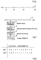
- Fig. 6 shows a schematic representation of a per se known message transmission device with a transmitter S, several receiving stations E1, E2, E3 ... Em and a bus, by means of which the transmitter S and the receiving stations E1 ... Em in series or ring circuit connected to each other.
- One transmitted by transmitter S over the bus Message therefore arrives at all receiving stations E1 ... Em a message sent by the sender S selectively to individual receiving stations can not be sent, does not contain the sent message only one composed of several bits message word but in addition, an address word composed of a number of bits.
- Each receiving device contains a device for checking, whether the address word of each message sent for the respective receiving point is acceptable or not. In the case of acceptance the message associated with this address word will be from the accepting receiving point.
- Fig. 7 shows a schematic representation of the known structure of a the receiving stations E1 ... Em.
- a receiving station has a physical interface 11, by means of which a bit acquisition of the carried over a bus 13 bit sequence is performed.
- the output signal the physical interface 11 is based on a so-called Protocol processing 15 given, by means of which a frame format detection and frame format checking is performed.
- the protocol processing 15 is followed by a message filter 17th with which an acceptance test is carried out, ie an examination, whether the respective transmitted address word of the considered Reception is accepted or not. If accepted, the with the message transmitted to the accepted address word to a consumer 19, which is a display device, an actuator or the like can act.
- the shown in Fig. 7 Circuitry is known per se.
- the present invention relates to an improvement of the message filter 17.
- FIG. 8 shows an example of two address words ADR0 and ADR1, which should be accepted by a specific receiving point.
- FIG. 9 shows a practical realization of an acceptance checking device, if there is only one acceptable address word and therefore only a single filter is needed.
- conventional Message filter for acceptance checking of two address words would require two filters with 12 filter bit locations each to check whether it is at the respectively transmitted data word to one of two acceptable data words or an unacceptable other Data word acts. So there would be two filters with a total of 24 Filter points required.
- a correspondingly large number of XOR gates and word lines on the Semiconductor chip needed in which this receiving point monolithically integrated is.
- FIG. 1 A first embodiment of a device according to the invention for Acceptance check or selection of address words is shown in FIG shown in schematic block diagram.
- each address word consists of 12 bit locations, each address word in 6 address word segments 2 bit positions is divided and the considered receiving point should accept two address words, as in the in Fig. 2 shown in the table as an example.
- Fig. 1 is a bit sequence of a frame-by-frame transmitted message each frame representing a frame start flag, an address field with 12 bit locations, an address field end tag bit and then a message word with a predetermined Bit length has.
- Fig. 1 of such a frame is substantially only the Address field for an address word with 12 address bit locations a0 to a11 and with a division into 6 address word segments (hereinafter also called segments for short) A to F with two bit positions each.
- the embodiment shown in Fig. 1 comprises a 4-out-of-2 decoder DEC with two decoder inputs DE1 and DE2 and four Decoder outputs DA0, DA1, DA2 and DA3.
- Each of the decoder outputs is an AND gate AND0, AND1, AND2 and AND3 assigned.
- Each of the filter registers has four filter register locations, each one of the AND gates AND0 are assigned to AND3.
- the outputs of the AND gates AND0 bis AND3 are each connected to an input of an OR gate OR, its output with the input side of a check result register He is connected.
- the check result register shows per Address word segment on a result register point, so a total six result register locations.
- An output of each of the result register locations is each with an input of another AND gate ANDT connected.
- At the output of an acceptance signal is removable, whose binary value depends on whether the respectively checked address word is acceptable or not.
- Fig. 1 below the address field, are the side of the check result register and an arrow is drawn on each side of the filter register, with which the demultiplex-like segmental processing of the respective Address word with the help of the 4-out-of-2 decoder DEC is indicated. That is, the two decoder inputs DE1 and DE2 are in one certain segment clock, the two segment bits of each segment A to F fed in succession. In the same segment clock are with the AND gates AND0 to AND3 the individual segments A to F associated filter register FRA to FRF connected in succession. And in the same segment clock at the OR gate OR segment by segment formed check result signals segment clockwise successively in the direction of the arrow in the individual result register locations of the transmission result register He enrolled. After checking the last segment of the respective received address word are then at the outputs of the 6 result register locations the 6 check result signals for the 6 segments A to F available.
- the decoder DEC supplies the logic value at its decoder output DA0 "1" if its inputs DE1 and DE2 the segment bit pattern "00" is supplied. For the segment bit pattern supplied to it on the input side "01", “10” and "11", the decoder DEC supplies a logic value "1" at the decoder output DA1 or DA2 or DA3. At each of these Segment bit pattern appears on the three other decoder outputs the logic value "0".
- the storage represents of the logic value "1" in the filter register location belonging to the AND gate AND0 a segment bit pattern "00" while the storage of the Logic value "1" in one of the AND gate AND 1 and AND2 and AND3 belonging register location a segment bit pattern "01" or "10” or "11" represents.
- FIG. 2 two are acceptable for a particular receiving location
- Address words ADR1 and ADR2 with an address word length of each 12 bits each, each in six segments A to F with two bit positions are divided.
- Fig. 3 shows the assignment of the filter register FRA to FRF for the case where the two address words shown in FIG from the selection or acceptance device according to FIG. 1 as acceptable to be evaluated. Since both address words ADR1 and ADR2 in segment A have the segment bit pattern "00" is located only in the left, belonging to the AND gate AND0 filter register location from FRA the logic value "1" while in the remaining three Filter register locations of FRA is the logic value "0".
- the logic value "1" is both in the AND gate AND1 and in the AND gate AND2 belonging second and third filter register location of FRB. In its two remaining digits is the logic value "0". In Similarly, in the filter registers FRC to FRF, the logic values "1" and "0" stored.
- Fig. 4 shows a dashed curve a verification process, if the receiving point considered the acceptable address word ADR1 supplied, and a solid course of a verification process, if the receiving station is the acceptable address word ADR2 is supplied.
- Fig. 4 in each of these both verification processes in the individual result register locations of the check result register ER shown.
- the decoder When the address word ADR1 is received, the decoder outputs while its decoder inputs DE1 and DE2 the segment bit pattern "00" of Address word segment A is supplied, the logic value "1" at its Decoder output DA0 off. As during the review of the segment A with the AND gates AND0 to AND3 the filter register of the Filter register FRA, appears at the output of AND0 the logic value "1” and is the OR gate OR the logic value "1" in the result register belonging to the segment A of the result register He wrote.
- Fig. 5 is a check process for an address word ADR3 that is not acceptable to those of the receiving point considered Address words heard.
- This address word ADR3 is correct all segments except the segment D with the address word ADR2 match. Therefore, the results register point assigned to the segment D appears the logic value "0" while in all others Result register locations of the logic value "1" appear. Because of the logic value "0" in the result register belonging to segment D. appears at the output of the AND gate ANDT the logic value "0", which on non-compliance of the address word ADR3 with one of acceptable address words ADR1 and ADR2, and thus non-acceptance the address word ADR3 signals.
Landscapes
- Engineering & Computer Science (AREA)
- Computer Security & Cryptography (AREA)
- Computer Networks & Wireless Communication (AREA)
- Signal Processing (AREA)
- Microelectronics & Electronic Packaging (AREA)
- Communication Control (AREA)
- Tests Of Electronic Circuits (AREA)
- Data Exchanges In Wide-Area Networks (AREA)
Claims (9)
- Dispositif pour la sélection de mots d'adresse (ADR1, ADR2, ADR3), qui présentent chacun n emplacements binaires et servent à l'adressage de m points de réception différents (E1, E2, ... Em) d'un appareil numérique de transmission d'informations, dans au moins l'un des points de réception, avec un appareil numérique d'acceptation, au moyen duquel des mots d'adresse (ADR1, ADR2) acceptables pour le point de réception considéré peuvent être sélectionnés et qui présente :a) un appareil de segmentation de mot d'adresse (DEC), au moyen duquel chaque mot d'adresse reçu par le point de réception peut être divisé en s segments de mot d'adresse (A à F) comprenant respectivement b emplacements binaires de segment, b étant égal à n/s et n étant un multiple entier de s ;b) un décodeur (DEC) avec une entrée de décodeur (DE1, DE2), auquel le modèle de bit du segment de mot d'adresse respectif du mot d'adresse qui est à vérifier au niveau de l'acceptation est amené pour le décodage selon un algorithme de décodage prédéfini, et une sortie de décodeur (DA0 à DA3), sur laquelle on peut prélever un modèle de bit de sortie de décodeur, représentant seulement un modèle de bit de segment, avec deux emplacements binaires pour chacun des modèles possibles de bit de segment ;c) s registres de filtre (FRA à FRF) attribués chacun à l'un des segments de mot d'adresse (A à F) pour le stockage de modèles de bit de registre de filtre dont chacun correspond au moins à l'un de tous les modèles de bit de sortie de décodeur, qui se forment lors du décodage de tous les modèles de bit de segment, qui peuvent apparaítre dans chaque segment correspondant de mot d'adresse de tous les mots d'adresse pouvant être acceptés par le point de réception considéré ;d) un appareil de comparaison (AND0 à AND3), au moyen duquel le modèle de bit de sortie de décodeur provenant du décodage du modèle de bit de segment du segment correspondant de mot d'adresse peut être comparé ensuite avec le contenu du registre de filtre correspondant (FRA à FRF), pour voir si le modèle de bit de sortie de décodeur provenant de l'opération de décodage respective coïncide ou non avec l'un des modèles de bit de registre de filtre mémorisés dans ce registre de filtre, et à la sortie desquels un signal de contrôle peut être prélevé, lequel est selon le résultat du contrôle un signal de concordance ("1") ou un signal de non-concordance ("0") ; ete) un appareil d'analyse (OR, ER, ANDT), qui fournit un signal d'acceptation ("1") après le décodage de tous les segments de mot d'adresse faisant partie du mot d'adresse respectivement reçu uniquement dans les cas où le signal de concordance (" 1") est apparu à la sortie de l'appareil de comparaison (ADN0 à AND3) pour chaque segment du mot d'adresse (A à F).
- Dispositif selon la revendication 1, sur lequela) le décodeur (DEC) présente b branchements d'entrée de décodeur (DE1, DE2), à chacun desquels l'un de ses b bits de segment peut être amené pendant chaque segment de mot d'adresse (A à F) et 2b branchements de sortie de décodeur (DA0 à DA3), sur lesquels apparaít un modèle de valeur binaire lors de chaque opération de décodage, de telle sorte qu'une première valeur binaire ("1") apparaít sur l'un des branchements de sortie de décodeur (DA0 à DA3) et la valeur binaire ("0") opposée apparaít sur tous les branchements de sortie de décodeur (DA0 à DA3) restants ;b) les registres de filtre (FRA à FRF) ont chacun 2b emplacements de registre de filtre, qui sont attribués chacun à l'un des 2b branchements de sortie de décodeur (DA0 à DA3), tous les emplacements de registre de filtre du stockage de la première valeur binaire ("1") servant dans chacun des registres de filtre (FRA à FRF), sur chacun des branchements de sortie de décodeur (DA0 à DA3) desquels, qui leur sont attribués, apparaít la première valeur binaire ("1") avec les modèles de bit de segment qui peuvent apparaítre dans tous les mots d'adresse (ADR1, ADR2) pouvant être acceptés par l'emplacement de réception considéré dans le segment de mot d'adresse (A à F), correspondant alors que les emplacements de registre de filtre restants de chaque registre de filtre (FRA à FRF) servent au stockage de la valeur binaire ("0") opposée, etc) l'appareil de comparaison (AND0 à AND3) fournit un signal de concordance ("1") pour le segment de mot d'adresse respectivement décodé dans les cas où la première valeur binaire ("1") se trouve dans l'emplacement de registre de filtre du registre de filtre (FRA à FRF) correspondant, lequel fait partie du branchement de sortie de décodeur (DA0 à DA3) qui fournit la première valeur binaire ("1") du modèle de bit de sortie de décodeur respectif
- Dispositif selon la revendication 2, sur lequel les segments de mot d'adresse (A à F) du mot d'adresse à vérifier respectivement au niveau de l'acceptation peuvent être amenés aux branchements d'entrée de décodeur (DA0 à DA3) dans l'ordre dans un cycle de segment et les registres de filtre (FRA à FRF) attribués aux segments de mot d'adresse (A à F) individuels peuvent être reliés dans l'ordre par bit de segment à l'appareil de comparaison (AND0 à AND3).
- Dispositif selon l'une quelconque des revendications 1 à 3, sur lequel est prévu un dispositif interrupteur, au moyen duquel les registres de filtre (FRA à FRF) individuels peuvent être reliés par cycle de segment dans l'ordre à l'appareil de comparaison (AND0 à AND3).
- Dispositif selon la revendication 3 ou 4, sur lequel l'appareil de comparaison présente 2b éléments ET (AND0 à AND3) avec respectivement deux entrées ET une sortie ET, une première entrée ET étant reliée pour chaque élément ET (AND0 à AND3) au branchement correspondant des branchements de sortie de décodeur (DA0 à DA3), et une autre entrée ET pouvant être reliée à l'emplacement de registre de filtre correspondant du registre de filtre (FRA à FRF) respectivement relié à l'appareil de comparaison (AND0 à AND3).
- Dispositif selon la revendication 5, sur lequel l'appareil d'analyse présente :a) un élément OU (OR) avec 2b entrées OU, qui sont reliées chacune à l'une des sorties ET, et une sortie OU, sur laquelle le signal de résultat de contrôle respectif peut être prélevé ;b) un registre de résultat de contrôle (ER) avec s emplacements de registre de résultat, dans lesquels les signaux du résultat du contrôle peuvent être inscrits par cycle de segment dans l'ordre pour les segments de mot d'adresse (A à F) individuels ; etc) un circuit ET (ANDT) avec s entrées de circuit ET, qui sont reliées chacune à l'un des emplacements du registre de résultat du registre de résultat de contrôle (ER), et une sortie de circuit ET, sur laquelle la première valeur binaire ("1") en cas d'acceptation du mot d'adresse contrôlé et la valeur binaire ("0") opposée en cas de non-acceptation peut être prélevée après le contrôle du dernier segment de mot d'adresse (A à F) du mot d'adresse respectif.
- Procédé pour la sélection de mots d'adresse, qui présentent n emplacements binaires et servent à l'adressage de m emplacements de réception différents d'un système numérique de transmission d'informations, dans au moins l'un des endroits de réception, avec lequel :a) chaque mot d'adresse est subdivisé en s segments de mot d'adresse (A à F) comprenant chacun b emplacements binaires de segment, b étant égal à n/s et n étant un multiple entier de s ;b) pour chaque segment de mot d'adresse (A à F), tous les modèles de bit de segment, qui peuvent apparaítre dans le segment de mot d'adresse respectif avec les mots d'adresse à accepter par le point de réception considéré, sont décodés selon un algorithme de décodage prédéfini en un modèle de valeur binaire présentant 2b emplacements binaires et ces modèles de valeur binaire sont mémorisés ;c) les modèles de bit de segment des différents segments de mots d'adresse du mot d'adresse respectivement reçu sont décodés dans un cycle de segment dans l'ordre selon l'algorithme de décodage prédéfini de façon appropriée en un modèle de valeur de codage présentant 2b emplacements binaires ;d) le modèle de valeur binaire respectivement obtenu lors du décodage est contrôlé au niveau de la concordance avec tous les modèles de valeur binaire mémorisés pour le segment de mot d'adresse respectif ; ete) après le contrôle de tous les segments de mot d'adresse d'un mot d'adresse reçu, on effectue à l'aide des résultats du contrôle pour les segments de mot d'adresse individuels de ce mot d'adresse une évaluation pour savoir s'il s'agit ou non en ce qui concerne le mot d'adresse respectivement reçu d'un mot d'adresse pouvant être accepté pour le point de réception considéré.
- Procédé selon la revendication 7, avec lequel le modèle de valeur binaire obtenu lors du décodage du segment de mot d'adresse respectif du mot d'adresse reçu et les modèles de valeur binaire acceptables et mémorisés pour ce segment de mot d'adresse sont soumis pour chaque emplacement binaire à une opération ET et le résultat du contrôle est déduit du résultat de l'opération ET.
- Procédé selon la revendication 8, avec lequel les résultats de l'opération ET obtenus pour chaque segment de mot d'adresse du mot d'adresse respectivement reçu sont mémorisés par segment et tous les résultats de l'opération ET, mémorisés après le contrôle du dernier segment de mot d'adresse du mot d'adresse respectivement reçu, sont soumis pour leur part à une opération ET, moyennant quoi on déduit du résultat de l'opération si le mot d'adresse respectivement reçu peut être accepté ou non par le point de réception considéré.
Applications Claiming Priority (2)
| Application Number | Priority Date | Filing Date | Title |
|---|---|---|---|
| DE19645057 | 1996-10-31 | ||
| DE19645057A DE19645057C2 (de) | 1996-10-31 | 1996-10-31 | Vorrichtung zur Selektion von Adressenwörtern mittels Demultiplex-Decodierung |
Publications (3)
| Publication Number | Publication Date |
|---|---|
| EP0840230A2 EP0840230A2 (fr) | 1998-05-06 |
| EP0840230A3 EP0840230A3 (fr) | 2002-03-06 |
| EP0840230B1 true EP0840230B1 (fr) | 2005-05-18 |
Family
ID=7810379
Family Applications (1)
| Application Number | Title | Priority Date | Filing Date |
|---|---|---|---|
| EP97118987A Expired - Lifetime EP0840230B1 (fr) | 1996-10-31 | 1997-10-30 | Dispositif et méthode de sélection de mots d'adresse utilisant du décodage de démultiplexage |
Country Status (3)
| Country | Link |
|---|---|
| US (1) | US6104728A (fr) |
| EP (1) | EP0840230B1 (fr) |
| DE (1) | DE19645057C2 (fr) |
Families Citing this family (6)
| Publication number | Priority date | Publication date | Assignee | Title |
|---|---|---|---|---|
| DE19809726A1 (de) * | 1998-03-06 | 1999-09-09 | Sgs Thomson Microelectronics | Interface für einen Datenknoten eines Datennetzes |
| US6529508B1 (en) * | 1999-02-01 | 2003-03-04 | Redback Networks Inc. | Methods and apparatus for packet classification with multiple answer sets |
| US20040153583A1 (en) * | 2001-09-20 | 2004-08-05 | Bartling James E. | Serial communication device with dynamic allocation of acceptance masks using serial implementation |
| US6944739B2 (en) * | 2001-09-20 | 2005-09-13 | Microchip Technology Incorporated | Register bank |
| US7274699B2 (en) * | 2002-09-20 | 2007-09-25 | Caterpillar Inc | Method for setting masks for message filtering |
| CN109145169B (zh) * | 2018-07-26 | 2021-03-26 | 浙江省测绘科学技术研究院 | 一种基于统计分词的地址匹配方法 |
Family Cites Families (10)
| Publication number | Priority date | Publication date | Assignee | Title |
|---|---|---|---|---|
| US4788507A (en) * | 1987-05-04 | 1988-11-29 | Eaton Corporation | Peak timeout indicator/encoder and method |
| EP0325670B1 (fr) * | 1988-01-28 | 1990-09-26 | Hewlett-Packard GmbH | Circuit détecteur de changement d'état de signaux binaires |
| EP0436194A3 (en) * | 1990-01-02 | 1992-12-16 | National Semiconductor Corporation | Media access controller |
| JP2695956B2 (ja) * | 1990-02-28 | 1998-01-14 | 株式会社東芝 | 多重通信システム |
| US5305321A (en) * | 1992-02-24 | 1994-04-19 | Advanced Micro Devices | Ethernet media access controller with external address detection interface and associated method |
| JP3208590B2 (ja) * | 1992-02-28 | 2001-09-17 | ソニー株式会社 | シリアル制御装置 |
| EP0663635A1 (fr) * | 1993-12-15 | 1995-07-19 | Firma Erika Köchler | Comparateur rapide pour données en série |
| US5467349A (en) * | 1993-12-21 | 1995-11-14 | Trw Inc. | Address handler for an asynchronous transfer mode switch |
| US5668525A (en) * | 1996-09-17 | 1997-09-16 | International Business Machines Corporation | Comparator circuit using two bit to four bit encoder |
| DE19645054C2 (de) * | 1996-10-31 | 1999-11-25 | Sgs Thomson Microelectronics | Vorrichtung und Verfahren zur Selektion von Adressenwörtern |
-
1996
- 1996-10-31 DE DE19645057A patent/DE19645057C2/de not_active Expired - Fee Related
-
1997
- 1997-10-30 US US08/960,846 patent/US6104728A/en not_active Expired - Lifetime
- 1997-10-30 EP EP97118987A patent/EP0840230B1/fr not_active Expired - Lifetime
Also Published As
| Publication number | Publication date |
|---|---|
| DE19645057A1 (de) | 1998-05-28 |
| EP0840230A3 (fr) | 2002-03-06 |
| US6104728A (en) | 2000-08-15 |
| EP0840230A2 (fr) | 1998-05-06 |
| DE19645057C2 (de) | 1999-11-25 |
Similar Documents
| Publication | Publication Date | Title |
|---|---|---|
| DE2751097C2 (de) | Schaltungsanordnung zum Erzeugen eines Kennsignals | |
| DE3300263C2 (fr) | ||
| DE2740483C2 (de) | Vorrichtung zur Feststellung von Merkmalen | |
| DE3407389C2 (fr) | ||
| DE2233796C3 (de) | Verfahren zur Video-Signal-Kompression und Expansion und Vorrichtungen zur Durchführung des Verfahrens | |
| DE2722124A1 (de) | Anordnung zum feststellen des prioritaetsranges in einem dv-system | |
| DE1474062B2 (de) | Datenverarbeitungsanlage mit einer anzahl von pufferspeichern | |
| DE3111555C2 (de) | Verfahren und Vorrichtung zur Informationsspeicherung unter Anwendung früherer Aufzeichnung | |
| EP0035731A2 (fr) | Procédé et dispositif pour le transfert de signaux de données | |
| DE2432608A1 (de) | Speicheranordnung fuer datenverarbeitungseinrichtungen | |
| DE2703559A1 (de) | Rechnersystem | |
| DE2736967A1 (de) | Asynchrone telemetrieschaltung | |
| EP0840230B1 (fr) | Dispositif et méthode de sélection de mots d'adresse utilisant du décodage de démultiplexage | |
| DE2062236A1 (de) | Verbesserungen an Redundanz Verringe rungssystemen und Einrichtungen zur Ver Wendung in diesen | |
| DE2556625B2 (de) | Anordnung zur Identifizierung von Objekten mit auf eine Abfrageimpulsgruppe mit einem Impulskode antwortender Bake | |
| EP0840229B1 (fr) | Dispositif et méthode de sélection de mots d'adresse | |
| DE3113189C2 (de) | Vorrichtung zur Umsetzung von digitalen Zeichencodes, die von einem Datenverarbeitungssystem empfangen oder geliefert werden | |
| EP0280914A2 (fr) | Appareil pour la réception de données | |
| EP0774849B1 (fr) | Procédé de transmission de données binaires, asynchrones, sur un canal synchrone | |
| EP0379625B1 (fr) | Procédé de traitement de mots binaires contrôlables par parité, qui, pendant leur transmission, subissent une atténuation numérique et/ou une conversion de code | |
| EP0427884A1 (fr) | Méthode et dispositif pour la compression et décompression de données | |
| EP0584387B1 (fr) | Procédé et circuit pour surveiller l'agencement de cellules pendant la transmission des cellules d'information | |
| DE2717065C3 (de) | Einrichtung zur Prüfung der Zuordnung einer Geheimzahl zu einer auf einer Karte gespeicherten Kartenzahl | |
| DE2641913C2 (de) | Schaltungsanordnung zur zyklischen Abfrage einer Vielzahl von Leitungen | |
| EP0377886B1 (fr) | Montage pour le transfert de mots de données subdivisés en plusieurs parties |
Legal Events
| Date | Code | Title | Description |
|---|---|---|---|
| PUAI | Public reference made under article 153(3) epc to a published international application that has entered the european phase |
Free format text: ORIGINAL CODE: 0009012 |
|
| AK | Designated contracting states |
Kind code of ref document: A2 Designated state(s): AT BE CH DE DK ES FI FR GB GR IE IT LI LU MC NL PT SE Kind code of ref document: A2 Designated state(s): FR GB IT |
|
| AX | Request for extension of the european patent |
Free format text: AL;LT;LV;RO;SI |
|
| PUAL | Search report despatched |
Free format text: ORIGINAL CODE: 0009013 |
|
| AK | Designated contracting states |
Kind code of ref document: A3 Designated state(s): AT BE CH DE DK ES FI FR GB GR IE IT LI LU MC NL PT SE |
|
| AX | Request for extension of the european patent |
Free format text: AL;LT;LV;RO;SI |
|
| RIC1 | Information provided on ipc code assigned before grant |
Free format text: 7G 06F 12/06 A, 7G 06F 7/02 B, 7H 04L 29/12 B |
|
| 17P | Request for examination filed |
Effective date: 20020410 |
|
| AKX | Designation fees paid |
Free format text: FR GB IT |
|
| REG | Reference to a national code |
Ref country code: DE Ref legal event code: 8566 |
|
| GRAP | Despatch of communication of intention to grant a patent |
Free format text: ORIGINAL CODE: EPIDOSNIGR1 |
|
| RTI1 | Title (correction) |
Free format text: APPARATUS AND METHOD FOR SELECTING ADDRESS WORDS USING DEMULTIPLEX-DECODING |
|
| GRAS | Grant fee paid |
Free format text: ORIGINAL CODE: EPIDOSNIGR3 |
|
| GRAA | (expected) grant |
Free format text: ORIGINAL CODE: 0009210 |
|
| AK | Designated contracting states |
Kind code of ref document: B1 Designated state(s): FR GB IT |
|
| REG | Reference to a national code |
Ref country code: GB Ref legal event code: FG4D Free format text: NOT ENGLISH |
|
| REG | Reference to a national code |
Ref country code: IE Ref legal event code: FG4D Free format text: LANGUAGE OF EP DOCUMENT: GERMAN |
|
| GBT | Gb: translation of ep patent filed (gb section 77(6)(a)/1977) |
Effective date: 20050802 |
|
| ET | Fr: translation filed | ||
| PLBE | No opposition filed within time limit |
Free format text: ORIGINAL CODE: 0009261 |
|
| STAA | Information on the status of an ep patent application or granted ep patent |
Free format text: STATUS: NO OPPOSITION FILED WITHIN TIME LIMIT |
|
| 26N | No opposition filed |
Effective date: 20060221 |
|
| PGFP | Annual fee paid to national office [announced via postgrant information from national office to epo] |
Ref country code: IT Payment date: 20061031 Year of fee payment: 10 |
|
| PG25 | Lapsed in a contracting state [announced via postgrant information from national office to epo] |
Ref country code: IT Free format text: LAPSE BECAUSE OF NON-PAYMENT OF DUE FEES Effective date: 20071030 |
|
| REG | Reference to a national code |
Ref country code: FR Ref legal event code: PLFP Year of fee payment: 20 |
|
| PGFP | Annual fee paid to national office [announced via postgrant information from national office to epo] |
Ref country code: GB Payment date: 20160928 Year of fee payment: 20 |
|
| PGFP | Annual fee paid to national office [announced via postgrant information from national office to epo] |
Ref country code: FR Payment date: 20160921 Year of fee payment: 20 |
|
| REG | Reference to a national code |
Ref country code: GB Ref legal event code: PE20 Expiry date: 20171029 |
|
| PG25 | Lapsed in a contracting state [announced via postgrant information from national office to epo] |
Ref country code: GB Free format text: LAPSE BECAUSE OF EXPIRATION OF PROTECTION Effective date: 20171029 |