EP0840230B1 - Apparatus and method for selecting address words using demultiplex-decoding - Google Patents
Apparatus and method for selecting address words using demultiplex-decoding Download PDFInfo
- Publication number
- EP0840230B1 EP0840230B1 EP97118987A EP97118987A EP0840230B1 EP 0840230 B1 EP0840230 B1 EP 0840230B1 EP 97118987 A EP97118987 A EP 97118987A EP 97118987 A EP97118987 A EP 97118987A EP 0840230 B1 EP0840230 B1 EP 0840230B1
- Authority
- EP
- European Patent Office
- Prior art keywords
- address word
- segment
- address
- bit
- locations
- Prior art date
- Legal status (The legal status is an assumption and is not a legal conclusion. Google has not performed a legal analysis and makes no representation as to the accuracy of the status listed.)
- Expired - Lifetime
Links
Images


Classifications
-
- G—PHYSICS
- G11—INFORMATION STORAGE
- G11C—STATIC STORES
- G11C8/00—Arrangements for selecting an address in a digital store
- G11C8/10—Decoders
-
- H—ELECTRICITY
- H04—ELECTRIC COMMUNICATION TECHNIQUE
- H04L—TRANSMISSION OF DIGITAL INFORMATION, e.g. TELEGRAPHIC COMMUNICATION
- H04L9/00—Cryptographic mechanisms or cryptographic arrangements for secret or secure communications; Network security protocols
- H04L9/40—Network security protocols
-
- Y—GENERAL TAGGING OF NEW TECHNOLOGICAL DEVELOPMENTS; GENERAL TAGGING OF CROSS-SECTIONAL TECHNOLOGIES SPANNING OVER SEVERAL SECTIONS OF THE IPC; TECHNICAL SUBJECTS COVERED BY FORMER USPC CROSS-REFERENCE ART COLLECTIONS [XRACs] AND DIGESTS
- Y10—TECHNICAL SUBJECTS COVERED BY FORMER USPC
- Y10S—TECHNICAL SUBJECTS COVERED BY FORMER USPC CROSS-REFERENCE ART COLLECTIONS [XRACs] AND DIGESTS
- Y10S707/00—Data processing: database and file management or data structures
- Y10S707/99931—Database or file accessing
- Y10S707/99933—Query processing, i.e. searching
- Y10S707/99936—Pattern matching access
Definitions
- the invention relates to a device and a method for selection address words (as described in EP-A-0 663 635) each having n bit positions and addressing from m different receiving stations of a digital communication device serve in at least one of the receiving points.
- the device comprises an acceptance device, by means of which the receiving point considered acceptable address words selectable are.
- each sent message for a particular receiving station is or is not determined in the Receiving point
- the address word of each message sent Correspondence with the data word assigned to this receiving point or the data words associated with this receiving station. This is conventionally done by means of filters as well how the address words have n bit positions and in which a bit sequence is stored, which corresponds to the bit sequence of an acceptable address word. If the receiving station in question should have multiple address words it needs as many filters with n bistels each as Address words should be acceptable.
- the address word of each of the single message offered message is with each bit string in each filter of this receiving station for conformity or non-conformity compared.
- Consumers are, for example, display devices or actuators.
- each of the plurality has Filter a receiving station a filter length equal to the address word length.
- this requires hardware with a capacity that one for cost reasons sometimes do not want to provide.
- the address register in which the address for the filter comparison caches the filters for comparison used XOR gates and the downstream of these OR gate many word lines required. These require on a chip of a monolithically integrated semiconductor circuit lots of space. Also XOR gates are circuit groups that take up a lot of space on a semiconductor chip.
- the present invention is based on the object, the circuit complexity for the acceptance check of received address words to reduce, in particular in a way, to the saving of Chip surface leads.
- a solution to this problem consists in a device according to Claim 1 and in a method according to claim 7. Preferred Embodiments thereof are given in the dependent claims.
- each address word is an address word of 12 bit locations and each address word in 6 address word segments is divided into 2 segment bit positions
- No XOR members are required which require more circuit complexity and chip area than AND gates. This huge saving on circuit units as well as word and Connecting leads to a huge reduction in the number of Such selection or acceptance device required area a semiconductor chip comprising this selection device monolithic integrated circuit.
- the decoder b has decoder input terminals to which one of its b segment bits can be supplied during each address word segment, and 2 b decoder output terminals at which a binary value pattern occurs in each decoding operation such that a first one at one of the decoder output terminals Binary value, for example "1", and at all remaining decoder output terminals of the opposite binary value, so for example, "0" occurs.
- the filter registers each have 2 b filter register locations which are each associated with one of the 2 b decoder output terminals, wherein in each of the filter registers all those filter register locations are used to store the first binary value at their respective assigned decoder output terminals in the segment bit patterns which are in all of the considered receiving location acceptable address words in the respective associated address word segment, the first binary value occurs while the remaining filter register locations of each filter register serve to store the opposite binary value.
- the comparator then provides a match signal for the respective decoded address word segment if the first binary value associated with the decoder output port providing the first binary value of the respective decoder output bit pattern is in that filter register location of the associated filter register.
- Address word can in turn address the decoder input terminals be deliverable in a segment clock and the individual address word segments associated filter registers are sequentially segmented clockwise connectable to the comparison device.
- the comparator 2 comprises b AND gates each having two AND inputs and one AND output, each AND gate having a first AND input connected to the respective one of the decoder output terminals, and another AND gate connected to each AND gate. Input with the respective corresponding filter register of each associated with the comparator filter register is connectable.
- the evaluation device has: an OR gate having 2 b OR inputs each connected to one of the AND outputs and an OR output to which the respective check result signal is detachable; a check result register with s result register locations, in which segment clockwise in turn the check result signals for the individual address word segments can be written; and an AND circuit with s AND circuit inputs, which are each connected to one of the result register locations, and an AND circuit output at which, after checking the last address word segment of the respective address word in the case of acceptance of the respectively checked address word of the first binary value and Non-acceptance of the opposite binary value is removable.
- the invention also provides a method for selecting address words each having n bit positions and serving for addressing m different receiving sites of a digital communication device in at least one of the receiving sites.
- For each address word segment all the segment bit patterns which can occur in the respective address words at the address words to be accepted by the receiving point under consideration are decoded into a binary value pattern having 2 b binary digits according to a predetermined decoding algorithm; the segment bit patterns of the individual address word segments of the respectively received address word are decoded in a segment clock in order, depending on the predetermined decoding algorithm, into a binary value pattern having 2 b binary digits; the binary value pattern respectively obtained by means of the decoding is checked for correspondence with all the binary value patterns stored for the respective address word segment; and after checking all the address word segments of a received address word on the basis of the verification results for the
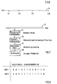
- Fig. 6 shows a schematic representation of a per se known message transmission device with a transmitter S, several receiving stations E1, E2, E3 ... Em and a bus, by means of which the transmitter S and the receiving stations E1 ... Em in series or ring circuit connected to each other.
- One transmitted by transmitter S over the bus Message therefore arrives at all receiving stations E1 ... Em a message sent by the sender S selectively to individual receiving stations can not be sent, does not contain the sent message only one composed of several bits message word but in addition, an address word composed of a number of bits.
- Each receiving device contains a device for checking, whether the address word of each message sent for the respective receiving point is acceptable or not. In the case of acceptance the message associated with this address word will be from the accepting receiving point.
- Fig. 7 shows a schematic representation of the known structure of a the receiving stations E1 ... Em.
- a receiving station has a physical interface 11, by means of which a bit acquisition of the carried over a bus 13 bit sequence is performed.
- the output signal the physical interface 11 is based on a so-called Protocol processing 15 given, by means of which a frame format detection and frame format checking is performed.
- the protocol processing 15 is followed by a message filter 17th with which an acceptance test is carried out, ie an examination, whether the respective transmitted address word of the considered Reception is accepted or not. If accepted, the with the message transmitted to the accepted address word to a consumer 19, which is a display device, an actuator or the like can act.
- the shown in Fig. 7 Circuitry is known per se.
- the present invention relates to an improvement of the message filter 17.
- FIG. 8 shows an example of two address words ADR0 and ADR1, which should be accepted by a specific receiving point.
- FIG. 9 shows a practical realization of an acceptance checking device, if there is only one acceptable address word and therefore only a single filter is needed.
- conventional Message filter for acceptance checking of two address words would require two filters with 12 filter bit locations each to check whether it is at the respectively transmitted data word to one of two acceptable data words or an unacceptable other Data word acts. So there would be two filters with a total of 24 Filter points required.
- a correspondingly large number of XOR gates and word lines on the Semiconductor chip needed in which this receiving point monolithically integrated is.
- FIG. 1 A first embodiment of a device according to the invention for Acceptance check or selection of address words is shown in FIG shown in schematic block diagram.
- each address word consists of 12 bit locations, each address word in 6 address word segments 2 bit positions is divided and the considered receiving point should accept two address words, as in the in Fig. 2 shown in the table as an example.
- Fig. 1 is a bit sequence of a frame-by-frame transmitted message each frame representing a frame start flag, an address field with 12 bit locations, an address field end tag bit and then a message word with a predetermined Bit length has.
- Fig. 1 of such a frame is substantially only the Address field for an address word with 12 address bit locations a0 to a11 and with a division into 6 address word segments (hereinafter also called segments for short) A to F with two bit positions each.
- the embodiment shown in Fig. 1 comprises a 4-out-of-2 decoder DEC with two decoder inputs DE1 and DE2 and four Decoder outputs DA0, DA1, DA2 and DA3.
- Each of the decoder outputs is an AND gate AND0, AND1, AND2 and AND3 assigned.
- Each of the filter registers has four filter register locations, each one of the AND gates AND0 are assigned to AND3.
- the outputs of the AND gates AND0 bis AND3 are each connected to an input of an OR gate OR, its output with the input side of a check result register He is connected.
- the check result register shows per Address word segment on a result register point, so a total six result register locations.
- An output of each of the result register locations is each with an input of another AND gate ANDT connected.
- At the output of an acceptance signal is removable, whose binary value depends on whether the respectively checked address word is acceptable or not.
- Fig. 1 below the address field, are the side of the check result register and an arrow is drawn on each side of the filter register, with which the demultiplex-like segmental processing of the respective Address word with the help of the 4-out-of-2 decoder DEC is indicated. That is, the two decoder inputs DE1 and DE2 are in one certain segment clock, the two segment bits of each segment A to F fed in succession. In the same segment clock are with the AND gates AND0 to AND3 the individual segments A to F associated filter register FRA to FRF connected in succession. And in the same segment clock at the OR gate OR segment by segment formed check result signals segment clockwise successively in the direction of the arrow in the individual result register locations of the transmission result register He enrolled. After checking the last segment of the respective received address word are then at the outputs of the 6 result register locations the 6 check result signals for the 6 segments A to F available.
- the decoder DEC supplies the logic value at its decoder output DA0 "1" if its inputs DE1 and DE2 the segment bit pattern "00" is supplied. For the segment bit pattern supplied to it on the input side "01", “10” and "11", the decoder DEC supplies a logic value "1" at the decoder output DA1 or DA2 or DA3. At each of these Segment bit pattern appears on the three other decoder outputs the logic value "0".
- the storage represents of the logic value "1" in the filter register location belonging to the AND gate AND0 a segment bit pattern "00" while the storage of the Logic value "1" in one of the AND gate AND 1 and AND2 and AND3 belonging register location a segment bit pattern "01" or "10” or "11" represents.
- FIG. 2 two are acceptable for a particular receiving location
- Address words ADR1 and ADR2 with an address word length of each 12 bits each, each in six segments A to F with two bit positions are divided.
- Fig. 3 shows the assignment of the filter register FRA to FRF for the case where the two address words shown in FIG from the selection or acceptance device according to FIG. 1 as acceptable to be evaluated. Since both address words ADR1 and ADR2 in segment A have the segment bit pattern "00" is located only in the left, belonging to the AND gate AND0 filter register location from FRA the logic value "1" while in the remaining three Filter register locations of FRA is the logic value "0".
- the logic value "1" is both in the AND gate AND1 and in the AND gate AND2 belonging second and third filter register location of FRB. In its two remaining digits is the logic value "0". In Similarly, in the filter registers FRC to FRF, the logic values "1" and "0" stored.
- Fig. 4 shows a dashed curve a verification process, if the receiving point considered the acceptable address word ADR1 supplied, and a solid course of a verification process, if the receiving station is the acceptable address word ADR2 is supplied.
- Fig. 4 in each of these both verification processes in the individual result register locations of the check result register ER shown.
- the decoder When the address word ADR1 is received, the decoder outputs while its decoder inputs DE1 and DE2 the segment bit pattern "00" of Address word segment A is supplied, the logic value "1" at its Decoder output DA0 off. As during the review of the segment A with the AND gates AND0 to AND3 the filter register of the Filter register FRA, appears at the output of AND0 the logic value "1” and is the OR gate OR the logic value "1" in the result register belonging to the segment A of the result register He wrote.
- Fig. 5 is a check process for an address word ADR3 that is not acceptable to those of the receiving point considered Address words heard.
- This address word ADR3 is correct all segments except the segment D with the address word ADR2 match. Therefore, the results register point assigned to the segment D appears the logic value "0" while in all others Result register locations of the logic value "1" appear. Because of the logic value "0" in the result register belonging to segment D. appears at the output of the AND gate ANDT the logic value "0", which on non-compliance of the address word ADR3 with one of acceptable address words ADR1 and ADR2, and thus non-acceptance the address word ADR3 signals.
Landscapes
- Engineering & Computer Science (AREA)
- Computer Security & Cryptography (AREA)
- Computer Networks & Wireless Communication (AREA)
- Signal Processing (AREA)
- Microelectronics & Electronic Packaging (AREA)
- Communication Control (AREA)
- Tests Of Electronic Circuits (AREA)
- Data Exchanges In Wide-Area Networks (AREA)
Description
Die Erfindung betrifft eine Vorrichtung und ein Verfahren zur Selektion von Adressenwörtern (wie im Dokument EP-A-0 663 635 beschrieben), die je n Bitstellen aufweisen und der Adressierung von m verschiedenen Empfangsstellen einer digitalen Nachrichtenübertragungseinrichtung dienen, in mindestens einer der Empfangsstellen. Die Vorrichtung umfaßt eine Akzeptanzeinrichtung, mittels welcher für die betrachtete Empfangsstelle akzeptierbare Adressenwörter selektierbar sind.The invention relates to a device and a method for selection address words (as described in EP-A-0 663 635) each having n bit positions and addressing from m different receiving stations of a digital communication device serve in at least one of the receiving points. The device comprises an acceptance device, by means of which the receiving point considered acceptable address words selectable are.
Es ist heutzutage üblich, bei einem System, das eine oder mehrere Sendestellen und mehrere Empfangsstellen aufweist, ein von einer Sendestelle ausgesendetes Signal an alle Empfangsstellen zu schicken, und zwar über einen gemeinsamen Übertragungskanal, beispielsweise in Form einer Busleitung. Damit die Möglichkeit besteht, von der Sendestelle Nachrichten nur an jeweils eine Empfangsstelle zu schicken, enthalten die von der Sendestelle gesendeten Signale jeweils zusätzlich zu der zu übertragenden Nachricht ein Adressenwort. Dabei ist jeder der Empfangsstellen mindestens ein für sie bestimmtes Adressenwort zugeordnet. Die einzelnen Empfangsstellen weisen Vorrichtungen zur Selektion der ihnen jeweils zugeordneten Adressenwörter auf. Daher kann diejenige Empfangsstelle, für welche die jeweils gesendete Nachricht bestimmt ist, solche Nachrichten aus dem Übertragungskanal entnehmen, welche mit einem für diese Empfangsstellen bestimmten oder akzeptierbaren Datenwort versehen ist.It is common nowadays for a system that has one or more senders and a plurality of receiving stations, one from a transmitting station send out transmitted signal to all receiving stations, and although via a common transmission channel, for example in Form of a bus line. So that there is the possibility of the transmitting station Messages only to one receiving station to send included the signals sent by the transmitting station in addition to the message to be transmitted an address word. Everybody is Receiving stations assigned at least one specific address word for them. The individual receiving points have devices for Selection of their respective assigned address words. Therefore can that receiving station for which the message sent is determined, remove such messages from the transmission channel, which with one intended for these receiving stations or acceptable data word is provided.
Gehören zu einer Empfangsstelle mehrere Empfänger, kann man jedem dieser Empfänger ein eigenes Adressenwort zuordnen. Sollen bestimmte Nachrichten von mehreren Empfangsstellen empfangbar sein, kann man so vorgehen, daß jede dieser Empfangsstellen nicht nur ihr eigenes Adressenwort akzeptiert sondern auch weitere Adressenwörter. In diesen Fällen wird die Empfangsstelle so ausgelegt, daß sie mehrere Adressenwörter akzeptieren kann.If you have several recipients at one receiving point, you can do it for everyone This receiver assign a separate address word. Should be certain You can receive messages from several receiving stations so that each of these receiving stations is not just their own Address word accepted but also more address words. In these Cases, the receiving station is designed so that they have multiple address words can accept.
Für die Überprüfung, ob das Adressenwort der über den Übertragungskanal, beispielsweise die Busleitung, jeweils gesendeten Nachricht für eine bestimmte Empfangsstelle bestimmt ist oder nicht, wird in der Empfangsstelle das Adressenwort der jeweils gesendeten Nachricht auf Übereinstimmung mit dem dieser Empfangsstelle zugeordneten Datenwort bzw. den dieser Empfangsstelle zugeordneten Datenwörtern verglichen. Dies geschieht herkömmlicherweise mittels Filtern, die genauso wie die Adressenwörter n Bitstellen aufweisen und in denen eine Bitfolge abgelegt ist, die der Bitfolge eines akzeptablen Adressenwortes entspricht. Soll die betrachtete Empfangstelle mehrere Adressenwörter akzeptieren können, benötigt sie soviele Filter mit je n Bistellen, wie Adressenwörter akzeptabel sein sollen. Das Adressenwort jeder der einzelnen Empfangsstelle angebotenen Nachricht wird mit jeder Bitfolge in jedem Filter dieser Empfangsstelle auf Übereinstimmung oder Nicht-Übereinstimmung verglichen. Besteht Übereinstimmung hinsichtlich eines der Filter, wird das gerade empfangene Adressenwort akzeptiert und die diesem Adressenwort beigepackte Nachricht zu Verbrauchereinheiten dieser Empfangsstelle durchgelassen. Stimmt das gerade empfangene Adressenwort nicht mit der in einem der Filter abgelegten Bitfolge überein, wird dieses Adressenwort nicht akzeptiert und gelangt die diesem Adressenwort beigepackte Nachricht nicht zu Verbrauchereinheiten dieser Empfangsstelle.For verifying that the address word is over the transmission channel, For example, the bus, each sent message for a particular receiving station is or is not determined in the Receiving point, the address word of each message sent Correspondence with the data word assigned to this receiving point or the data words associated with this receiving station. This is conventionally done by means of filters as well how the address words have n bit positions and in which a bit sequence is stored, which corresponds to the bit sequence of an acceptable address word. If the receiving station in question should have multiple address words it needs as many filters with n bistels each as Address words should be acceptable. The address word of each of the single message offered message is with each bit string in each filter of this receiving station for conformity or non-conformity compared. Consists of agreement one of the filters, the address word just received is accepted and the message to consumer units enclosed with this address word passed through this receiving station. Is that just received Address word not with the one stored in one of the filters Bit string match, this address word is not accepted and gets the message enclosed with this address word not to consumer units this receiving point.
Verbraucher sind beispielsweise Anzeigevorrichtungen oder Stellglieder.Consumers are, for example, display devices or actuators.
Für den Vergleich, ob ein empfangenes Adressenwort mit der in dem
Filter abgelegten Bitfolge übereinstimmt oder nicht, werden herkömmlicherweise
XOR-Verknüpfungsschaltungen verwendet, und zwar pro
Bitstelle von Adressenwort und Filter eine. Weist das Adressenwort
beispielsweise 12 Bitstellen auf, besitzt auch das Filter 12 Bitstellen und
sind für den Vergleich des jeweils empfangenen Adressenwortes mit der
in dem Filter abgelegten Bitfolge 12 XOR-Verknüpfungsschaltungen
erforderlich. Die Ausgänge sämtlicher XOR-Verknüpfungsglieder werden
auf ein OR-Verknüpfungsglied gegeben, das soviele Eingänge aufweist,
wie XOR-Verknüpfungsglieder vorhanden sind. An einem Ausgang
des OR-Verknüpfungsgliedes erscheint je nach dem, ob zwischen
dem gerade empfangenen Adressenwort und dem in dem Filter abgelegten
Wort Übereinstimmung besteht oder nicht, der Logikwert "1" oder
der Logikwert "0". Der Logikwert "0" am Ausgang des OR-Verknüpfungsgliedes
bedeutet somit, daß das gerade empfangene Adressenwort
von der betrachteten Empfangsstelle akzeptiert wird, während es nicht
akzeptiert wird, wenn am Ausgang des OR-Verknüpfungsgliedes der
Logikwert "1" erscheint.For comparing whether a received address word with that in the
Filter stored bit sequence matches or not, become conventional
XOR gate circuits used, per
Bit position of address word and filter one. Indicates the address word
For example, 12 bit positions, the filter also has 12 bit positions and
are for the comparison of each received address word with the
in the filter stored
Bei der zuvor betrachteten herkömmlichen Lösung hat jedes der mehreren Filter einer Empfangsstelle eine Filterlänge gleich der Adressenwortlänge. Dies erfordert einerseits Hardware mit einer Kapazität, die man aus Kostengründen mitunter nicht bereitstellen möchte. Andererseits sind zwischen dem Adressenregister, in dem die Adresse für den Filtervergleich zwischengespeichert wird, den Filtern, den für den Vergleich verwendeten XOR-Verknüpfungsgliedern und dem diesen nachgeschalteten OR-Verknüpfungsglied viele Wortleitungen erforderlich. Diese erfordern auf einem Chip einer monolithisch integrierten Halbleiterschaltung viel Platz. Auch XOR-Verknüpfungsglieder sind Schaltungsgruppen, die relativ viel Platz auf einem Halbleiterchip beanspruchen.In the conventional solution considered above, each of the plurality has Filter a receiving station a filter length equal to the address word length. On the one hand, this requires hardware with a capacity that one for cost reasons sometimes do not want to provide. on the other hand are between the address register, in which the address for the filter comparison caches the filters for comparison used XOR gates and the downstream of these OR gate many word lines required. These require on a chip of a monolithically integrated semiconductor circuit lots of space. Also XOR gates are circuit groups that take up a lot of space on a semiconductor chip.
Der vorliegenden Erfindung liegt die Aufgabe zugrunde, den Schaltungsaufwand für die Akzeptanzprüfung von empfangenen Adressenwörtern zu reduzieren, insbesondere auf eine Weise, die zur Einsparung von Chipfläche führt.The present invention is based on the object, the circuit complexity for the acceptance check of received address words to reduce, in particular in a way, to the saving of Chip surface leads.
Eine Lösung dieser Aufgabe besteht in einer Vorrichtung gemäß
Anspruch 1 und in einem Verfahren gemäß Anspruch 7. Bevorzugte
Ausführungsformen hiervon sind in den abhängigen Ansprüchen angegeben. A solution to this problem consists in a device according to
Die Erfindung schafft eine Vorrichtung, mittels welcher sich in einer Empfangsstelle einer digitalen Nachrichtenübertragungseinrichtung Adressenwörter selektieren lassen, die je n Bitstellen aufweisen und der Adressierung von m verschiedenen Empfangsstellen der Nachrichtenübertragungseinrichtung dienen. Die Vorrichtung umfaßt eine digitale Akzeptanzeinrichtung, mittels welcher für die betrachtete Empfangsstelle akzeptierbare Adressenwörter selektierbar sind. Die Akzeptanzeinrichtung weist auf:
- eine Adressenwortsegmentiereinrichtung, mittels welcher jedes von der Empfangsstelle empfangene Adressenwort in s Adressenwortsegmente mit je b Segmentbitstellen unterteilbar ist, wobei b = n/s und n ein ganzzahliges Vielfaches von s ist;
- einen Decoder mit einem Decodereingang, dem das Segmentbitmuster des jeweiligen Adressenwortsegmentes des jeweils auf Akzeptanz zu überprüfenden Adressenwortes zur Decodierung nach einem vorbestimmten Decodieralgorithmus zuführbar ist, und einen Decoderausgang, an dem für jedes der möglichen Segmentbitmuster ein nur dieses Segmentbitmuster repräsentierendes Decoderausgangsbitmuster mit 2b Binärstellen abnenmbar ist;
- s je einem der Adressenwortsegmente zugeordnete Filterregister zur Speicherung von Filterregisterbitmustern, von denen jedes einem von all denjenigen Decoderausgangsbitmustern entspricht, die beim Decodieren all derjenigen Segmentbitmuster entstehen, welche im je zugehörigen Adressenwortsegment aller von der betrachteten Empfangsstelle akzeptierbaren Adressenwörter auftreten können;
- eine Vergleichseinrichtung, mittels welcher das aus der Decodierung des Segmentbitmusters des jeweiligen Adressenwortsegmentes hervorgehende Decoderausgangsbitmuster mit dem Inhalt des je zugehörigen Filterregisters daraufhin überprüfbar ist, ob das aus dem jeweiligen Decodiervorgang hervorgegangene Decoderausgangsbitmuster mit einem der in diesem Filterregister gespeicherten Filterregisterbitmuster übereinstimmt oder nicht, und an deren Ausgang jeweils ein Überprüfungsergebnissignal abnehmbar ist, das je nach dem Überprüfungsergebnis ein Übereinstimmungssignal oder ein Nicht-Übereinstimmungssignal ist;
- und eine Auswertungseinrichtung, welche nach der Decodierung aller zu dem jeweils empfangenen Adressenwort gehörender Adressenwortsegmente ein Akzeptanzsignal nur dann liefert, wenn am Ausgang der Vergleichseinrichtung für jedes Adressenwortsegment dieses Adressenwortes ein Übereinstimmungssignal aufgetreten ist.
- an address word segmenting device, by means of which each address word received by the receiving point can be subdivided into s address word segments having b segment bit positions each, where b = n / s and n is an integer multiple of s;
- a decoder with a decoder input to which the segment bit pattern of the respective address word segment of the respectively to be checked for acceptance address word for decoding according to a predetermined decoding algorithm can be supplied, and a decoder output, at which for each of the possible segment bit pattern a only this segment bit pattern representing decoder output bit pattern with 2 b binary points abnenmbar is;
- s each one of the address word segments associated filter registers for storing Filterregisterbitmustern, each of which corresponds to one of all those Decoderausgangsbitmustern that arise when decoding all those Segmentbitmuster that can occur in each associated address word segment of all acceptable by the considered receiving point address words;
- a comparison device, by means of which the decoder output bit pattern resulting from the decoding of the segment bit pattern of the respective address word segment can be checked with the content of the respective associated filter register as to whether the decoder output bit pattern resulting from the respective decoding process coincides with one of the filter register bit patterns stored in this filter register and at the latter Output is each a check result signal is removable, which is a match signal or a non-match signal depending on the result of the check;
- and an evaluation device which, after the decoding of all address word segments belonging to the respectively received address word, only delivers an acceptance signal if a match signal has occurred at the output of the comparison device for each address word segment of this address word.
Möchte man bei der bekannten Akzeptanzprüfungsmethode für eine bestimmte Empfangsstelle beispielsweise zwei verschiedene Adressenwörter akzeptieren, muß man in dieser Empfangsstelle zwei Filter vorsehen, die je eine Filterlänge gleich der Adressenwortlänge aufweisen. Bei einer Adressenwortlänge von beispielsweise 12 Bitstellen benötigt man in diesem Fall 24 Filterstellen. Hinzu kommt eine entsprechend große Anzahl von XOR-Gliedern und von Wortleitungen mit entsprechend hohem Platzbedarf auf dem Halbleiterchip, auf dem sich die Adressenselektionsvorrichtung befindet.Would you like the known acceptance test method for a For example, certain receiving location two different address words you have to accept two filters in this receiving station provide that each have a filter length equal to the address word length. For an address word length of, for example, 12 bit positions needed in this case 24 filter points. There is also a corresponding large number of XOR gates and word lines with accordingly high space requirement on the semiconductor chip on which the Address selection device is located.
Bei der erfindungsgemäßen segmentweisen Überprüfung der empfangenen Adressenwörter auf Akzeptanz kommt man mit wesentlich weniger Schaltungselementen und mit wesentlich weniger Wortleitungen aus. Nimmt man beispielsweise an, daß jedes Adressenwort eine Adressenwordänge von 12 Bitstellen aufweist und jedes Adressenwort in 6 Adressenwortsegmente à 2 Segmentbitstellen unterteilt ist, benötigt man bei einer bevorzugten Ausführungsform lediglich einen 4-aus-2-Decoder mit zwei Eingangsleitungen und vier Ausgangsleitungen, 4 UND-Glieder, 6 Filterregister à 4 Filterregisterstellen sowie eine Auswertungseinrichtung zur Auswertung der UND-Verknüpfungsergebnisse, die im Prizip wie im herkömmlichen Fall aufgebaut, jedoch wesentlich weniger komplex sind, da sie nicht 32 Vergleichsergebnisse auszuwerten braucht sondern lediglich 4 Vergleichsergebnisse. Es sind keine XOR-Glieder erforderlich, die mehr Schaltungsaufwand und Chipfläche benötigen als UND-Glieder. Diese gewaltige Einsparung an Schaltungseinheiten sowie Wort- und Verbindungsleitungen führt zu einer gewaltigen Reduzierung der für eine solche Selektions- oder Akzeptanzvorrichtung erforderlichen Fläche auf einem Halbleiterchip einer diese Selektionsvorrichtung umfassenden monolithisch integrierten Schaltung.In the inventive segment-by-segment verification of the received Address words for acceptance can be obtained with much less Circuit elements and with significantly fewer word lines. For example, assume that each address word is an address word of 12 bit locations and each address word in 6 address word segments is divided into 2 segment bit positions, you need at a preferred embodiment, only a 4-of-2 decoder with two input lines and four output lines, 4 AND gates, 6 Filter register with 4 filter register locations as well as an evaluation device for the evaluation of the AND-linking results, which in the Prizip as in built in a conventional case, but are much less complex, since she does not need to evaluate 32 comparison results but only 4 comparison results. No XOR members are required which require more circuit complexity and chip area than AND gates. This huge saving on circuit units as well as word and Connecting leads to a huge reduction in the number of Such selection or acceptance device required area a semiconductor chip comprising this selection device monolithic integrated circuit.
Bei einer bevorzugten Ausführungsform der Erfindung weist der Decoder b Decodereingangsanschlüsse auf, denen während eines jeden Adressenwortsegments je eines von dessen b Segmentbits zuführbar ist, sowie 2b Decoderausgangsanschlüsse, an denen bei jedem Decodiervorgang ein Binärwertmuster auftritt, derart, daß an einem der Decoderausgangsanschlüsse ein erster Binärwert, beispielsweise "1", und an allen restlichen Decoderausgangsanschlüssen der entgegengesetzte Binärwert, also beispielsweise "0", auftritt. Die Filterregister weisen je 2b Filterregisterstellen auf, die je einem der 2b Decoderausgangsanschlüsse zugeordnet sind, wobei in jedem der Filterregister alle diejenigen Filterregisterstellen der Speicherung des ersten Binärwertes dienen, an deren je zugeordneten Decoderausgangsanschlüssen bei den Segmentbitmustern, die in allen von der betrachteten Empfangsstelle akzeptierbaren Adressenwörtern in dem je zugehörigen Adressenwortsegment auftreten können, der erste Binärwert auftritt, während die restlichen Filterregisterstellen eines jeden Filterregisters der Speicherung des entgegengesetzten Binärwertes dienen. Die Vergleichseinrichtung liefert für das jeweils decodierte Adressenwortsegment dann ein Übereinstimmungssignal, wenn sich in derjenigen Filterregisterstelle des zugehörigen Filterregisters der erste Binärwert befindet, welche zu dem Decoderausgangsanschluß gehört, der den ersten Binärwert des jeweiligen Decoderausgangbitmusters liefert.In a preferred embodiment of the invention, the decoder b has decoder input terminals to which one of its b segment bits can be supplied during each address word segment, and 2 b decoder output terminals at which a binary value pattern occurs in each decoding operation such that a first one at one of the decoder output terminals Binary value, for example "1", and at all remaining decoder output terminals of the opposite binary value, so for example, "0" occurs. The filter registers each have 2 b filter register locations which are each associated with one of the 2 b decoder output terminals, wherein in each of the filter registers all those filter register locations are used to store the first binary value at their respective assigned decoder output terminals in the segment bit patterns which are in all of the considered receiving location acceptable address words in the respective associated address word segment, the first binary value occurs while the remaining filter register locations of each filter register serve to store the opposite binary value. The comparator then provides a match signal for the respective decoded address word segment if the first binary value associated with the decoder output port providing the first binary value of the respective decoder output bit pattern is in that filter register location of the associated filter register.
Die Adressenwortsegmente des jeweils auf Akzeptanz zu überprüfenden Adressenwortes können den Decodereingangsanschlüssen der Reihe nach in einem Segmenttakt zuführbar sein und die den einzelnen Adressenwortsegmenten zugeordneten Filterregister sind der Reihe nach segmenttaktweise mit der Vergleichseinrichtung verbindbar. The address word segments of each to be checked for acceptance Address word can in turn address the decoder input terminals be deliverable in a segment clock and the individual address word segments associated filter registers are sequentially segmented clockwise connectable to the comparison device.
Bei einer Ausführungsform der Erfindung weist die Vergleichseinrichtung
2b UND-Glieder mit je zwei UND-Eingängen und einem UND-Ausgang
auf, wobei bei jedem UND-Glied ein erster UND-Eingang mit
dem je entsprechenden der Decoderausgangsanschlüsse verbunden ist
und ein anderer UND-Eingang mit der je entsprechenden Filterregisterstelle
des jeweils mit der Vergleichseinrichtung verbundenen Filterregisters
verbindbar ist.In one embodiment of the invention, the
Bei einer Ausführungsform der Erfindung weist die Auswertungseinrichtung
auf:
ein ODER-Glied mit 2b ODER-Eingängen, die je mit einem der UND-Ausgänge
verbunden sind, und einem ODER-Ausgang, an dem das
jeweilige Überprüfungsergebnissignal abnehmbar ist; ein Überprüfungsergebnisregister
mit s Ergebnisregisterstellen, in welche segmenttaktweise
der Reihe nach die Überprüfungsergebnissignale für die einzelnen
Adressenwortsegmente einschreibbar sind; und eine UND-Schaltung mit
s UND-Schaltungseingängen, die mit je einer der Ergebnisregisterstellen
verbunden sind, und einem UND-Schaltungsausgang, an dem nach der
Überprüfung des letzten Adressenwortsegmentes des jeweiligen Adressenwortes
im Fall der Akzeptanz des jeweils überprüften Adressenwortes
der erste Binärwert und bei Nicht-Akzeptanz der entgegengesetzte Binärwert
abnehmbar ist.In one embodiment of the invention, the evaluation device has:
an OR gate having 2 b OR inputs each connected to one of the AND outputs and an OR output to which the respective check result signal is detachable; a check result register with s result register locations, in which segment clockwise in turn the check result signals for the individual address word segments can be written; and an AND circuit with s AND circuit inputs, which are each connected to one of the result register locations, and an AND circuit output at which, after checking the last address word segment of the respective address word in the case of acceptance of the respectively checked address word of the first binary value and Non-acceptance of the opposite binary value is removable.
Es kann eine Schaltereinrichtung vorgesehen sein, mittels welcher die einzelnen Filterregister segmenttaktweise der Reihe nach mit der Vergleichseinrichtung verbindbar sind.It may be provided a switch means by which the individual filter register segment clockwise in turn with the comparator are connectable.
Die Erfindung macht außerdem ein Verfahren verfügbar zur Selektion von Adressenwörtern, die je n Bitstellen aufweisen und der Adressierung von m verschiedenen Empfangsstellen einer digitalen Nachrichtenübertragungseinrichtung dienen, in mindestens einer der Empfangsstellen. Dabei wird jedes Adressenwort in s Adressenwortsegmente mit je b segmentbitstellen unterteilt, wobei b=n/s und n ein ganzzahliges Vielfaches von s ist; werden für jedes Adressenwortsegment alle Segmentbitmuster, die bei den von der betrachteten Empfangsstelle zu akzeptierenden Adressenwörtern in dem jeweiligen Adressenwort vorkommen können, nach einem vorbestimmten Decodieralgorithmus in ein 2b Binärstellen aufweisendes Binärwertmuster decodiert; werden die Segmentbitmuster der einzelnen Adressenwortsegmente des jeweils empfangenen Adressenwortes in einem Segmenttakt der Reihe nach je nach dem vorbestimmten Decodieralgorithmus in ein 2b Binärstellen aufweisendes Binärwertmuster decodiert; wird das mittels der Decodierung jeweils erhaltene Binärwertmuster mit allen für das jeweilige Adressenwortsegment gespeicherten Binärwertmustern auf Übereinstimmung überprüft; und wird nach Überprüfung aller Adressenwortsegmente eines empfangenen Adressenwortes anhand der Überprüfungsergebnisse für die einzelnen Adressenwortsegmente für dieses Adressenwort eine Bewertung dahingehend durchgeführt, ob es sich bei dem jeweils empfangenen Adressenwort um ein für die betrachtete Empfangsstelle akzeptierbares Adressenwort handelt oder nicht.The invention also provides a method for selecting address words each having n bit positions and serving for addressing m different receiving sites of a digital communication device in at least one of the receiving sites. In this case, each address word is subdivided into s address word segments with each segmental digit b, where b = n / s and n is an integer multiple of s; For each address word segment, all the segment bit patterns which can occur in the respective address words at the address words to be accepted by the receiving point under consideration are decoded into a binary value pattern having 2 b binary digits according to a predetermined decoding algorithm; the segment bit patterns of the individual address word segments of the respectively received address word are decoded in a segment clock in order, depending on the predetermined decoding algorithm, into a binary value pattern having 2 b binary digits; the binary value pattern respectively obtained by means of the decoding is checked for correspondence with all the binary value patterns stored for the respective address word segment; and after checking all the address word segments of a received address word on the basis of the verification results for the individual address word segments for this address word an assessment is made as to whether or not the respectively received address word is an acceptable for the receiving point considered address word.
Dabei können das bei der Decodierung des jeweiligen Adressenwortsegmentes des empfangenen Adressenwortes erhaltene Binärwertmuster und die für dieses Adressenwortsegment gespeicherten akzeptablen Binärwertmuster bitstellenweise einer UND-Verknüfung unterzogen werden und kann das Überprüfungsergebnis aus dem UND-Verknüfungsergebnis abgeleitet werden. Die für jedes Adressenwortsegment des jeweils empfangenen Adressenwortes erhaltenen UND-Verknüfungsergebnisse können segmentweise gespeichert werden und alle nach der Überprüfung des letzten Adressenwortsegmentes des jeweils empfangenen Adressenwortes gespeicherten UND-Verknüfungsergebnisse können ihrerseits einer UND-Verknüfung unterzogen werden, wobei von deren Verknüpfungsergebnis ableitbar ist, ob das jeweils empfangene Adressenwort von der betrachteten Empfangsstelle akzeptierbar ist oder nicht. This can be done in the decoding of the respective address word segment of the received address word obtained binary value pattern and the acceptable binary value pattern stored for this address word segment be bit-wise AND-linked and can the check result from the AND match result be derived. The for each address word segment of each received Address word AND correlation results can be saved segment by segment and all after verification the last address word segment of the respective received address word saved AND link results can be your turn be subjected to an AND-linking, whereby of their connection result can be deduced whether the respectively received address word is acceptable from the receiving point considered or not.
Die Erfindung wird nun anhand von Ausführungsformen näher erläutert.
In den Zeichnungen zeigen:
Fig. 6 zeigt in schematisierter Darstellung eine an sich bekannte Nachrichtenübertragungseinrichtung mit einem Sender S, mehreren Empfangsstellen E1, E2, E3 ... Em und einem Bus, mittels welchem der Sender S und die Empfangsstellen E1 ... Em in Reihen- oder in Ringschaltung miteinander verbunden sind. Eine vom Sender S über den Bus übertragene Nachricht gelangt daher an alle Empfangsstellen E1 ... Em. Damit eine vom Sender S gesendete Nachricht selektiv an einzelne Empfangsstellen geschickt werden kann, enthält die ausgesendete Nachricht nicht nur ein aus mehreren Bits zusammengesetztes Nachrichtenwort sondern zusätzlich ein aus einer Anzahl von Bits zusammengesetztes Adressenwort. Jede Empfangsvorrichtung enthält eine Vorrichtung zur Überprüfung, ob das Adressenwort der jeweils gesendeten Nachricht für die jeweilige Empfangsstelle akzeptierbar ist oder nicht. Im Fall der Akzeptanz wird die mit diesem Adressenwort verknüpfte Nachricht von der akzeptierenden Empfangsstelle übernommen.Fig. 6 shows a schematic representation of a per se known message transmission device with a transmitter S, several receiving stations E1, E2, E3 ... Em and a bus, by means of which the transmitter S and the receiving stations E1 ... Em in series or ring circuit connected to each other. One transmitted by transmitter S over the bus Message therefore arrives at all receiving stations E1 ... Em a message sent by the sender S selectively to individual receiving stations can not be sent, does not contain the sent message only one composed of several bits message word but in addition, an address word composed of a number of bits. Each receiving device contains a device for checking, whether the address word of each message sent for the respective receiving point is acceptable or not. In the case of acceptance the message associated with this address word will be from the accepting receiving point.
Fig. 7 zeigt in schematischer Darstellung den bekannten Aufbau einer
der Empfangsstellen E1 ... Em. Eine solche Empfangsstelle besitzt eine
physikalische Schnittstelle 11, mittels welcher eine Bitübernahme der
über einen Bus 13 übertragenen Bitfolge durchgeführt wird. Das Ausgangssignal
der physikalischen Schnittstelle 11 wird auf eine sogenannte
Protokollabwicklung 15 gegeben, mittels welcher eine Rahmenformat-Erkennung
und Rahmenformat-Prüfung durchgeführt wird. An den Ausgang
der Protokollabwicklung 15 schließt sich ein Nachrichtenfilter 17
an, mit dem eine Akzeptanzprüfung durchgeführt wird, also eine Prüfung,
ob das jeweils übertragene Adressenwort von der betrachteten
Empfangsstelle akzeptiert wird oder nicht. Bei Akzeptanz wird die mit
dem akzeptierten Adressenwort übertragene Nachricht an einen Verbraucher
19 weitergegeben, bei dem es sich um eine Anzeigevorrichtung,
ein Stellglied oder ähnliches handeln kann. Der in Fig. 7 gezeigte
Schaltungsaufbau ist an sich bekannt. Die vorliegende Erfindung bezieht
sich auf eine Verbesserung des Nachrichtenfilters 17.Fig. 7 shows a schematic representation of the known structure of a
the receiving stations E1 ... Em. Such a receiving station has a
Fig. 8 zeigt ein Beispiel von zwei Adressenwörtern ADR0 und ADR1, die von einer bestimmten Empfangsstelle akzeptiert werden sollen. Fig. 9 zeigt eine praktische Realisierung einer Akzeptanzüberprüfungseinrichtung, wenn es nur ein akzeptierbares Adressenwort gibt und daher nur ein einziges Filter benötigt wird. Bei Anwendung herkömmlicher Nachrichtenfilter zur Akzeptanzüberprüfung von zwei Adressenwörtern wären zwei Filter mit je 12 Filterbitstellen erforderlich, um zu überprüfen, ob es sich bei dem jeweils übertragenen Datenwort um eines der zwei akzeptierbaren Datenwörter oder um ein nicht-akzeptierbares sonstiges Datenwort handelt. Es wären also zwei Filter mit insgesamt 24 Filterstellen erforderlich. Außerdem wird eine entsprechend große Anzahl von XOR-Verknüpfungsschaltungen und von Wortleitungen auf dem Halbleiterchip benötigt, in dem diese Empfangsstelle monolithisch integriert ist.Fig. 8 shows an example of two address words ADR0 and ADR1, which should be accepted by a specific receiving point. FIG. 9 shows a practical realization of an acceptance checking device, if there is only one acceptable address word and therefore only a single filter is needed. When using conventional Message filter for acceptance checking of two address words would require two filters with 12 filter bit locations each to check whether it is at the respectively transmitted data word to one of two acceptable data words or an unacceptable other Data word acts. So there would be two filters with a total of 24 Filter points required. In addition, a correspondingly large number of XOR gates and word lines on the Semiconductor chip needed in which this receiving point monolithically integrated is.
Eine erste Ausführungsform einer erfindungsgemäßen Vorrichtung zur Akzeptanzprüfung oder Selektion von Adressenwörtern ist in Fig. 1 in schematischer Blockdarstellung gezeigt.A first embodiment of a device according to the invention for Acceptance check or selection of address words is shown in FIG shown in schematic block diagram.
Bei dieser Ausführungsform wird davon ausgegangen, daß jedes Adressenwort
aus 12 Bitstellen besteht, jedes Adressenwort in 6 Adressenwortsegmente
ä 2 Bitstellen unterteilt ist und die betrachtete Empfangsstelle
zwei Adressenwörter akzeptieren soll, wie sie in der in Fig. 2
gezeigten Tabelle als Beispiel angegeben sind.In this embodiment, it is assumed that each address word
consists of 12 bit locations, each address word in 6
In Fig. 1 oben ist eine Bitfolge einer rahmenweise übertragenen Nachricht dargestellt, wobei jeder Rahmen ein Rahmenstart-Kennzeichnungsbit, ein Adressenfeld mit 12 Bitstellen, ein Adressenfeldende-Kennzeichnungsbit und daran anschließend ein Nachrichtenwort mit vorbestimmter Bitlänge aufweist.In Fig. 1 above is a bit sequence of a frame-by-frame transmitted message each frame representing a frame start flag, an address field with 12 bit locations, an address field end tag bit and then a message word with a predetermined Bit length has.
In Fig. 1 ist von einem derartigen Rahmen im wesentlichen nur das Adressenfeld für ein Adressenwort mit 12 Adressenbitstellen a0 bis a11 und mit einer Unterteilung in 6 Adressenwortsegmente (im folgenden auch kurz Segmente genannt) A bis F mit je zwei Bitstellen dargestellt.In Fig. 1 of such a frame is substantially only the Address field for an address word with 12 address bit locations a0 to a11 and with a division into 6 address word segments (hereinafter also called segments for short) A to F with two bit positions each.
Die in Fig. 1 dargestellte Ausführungsform umfaßt einen 4-aus-2-Decoder DEC mit zwei Decodereingängen DE1 und DE2 und mit vier Decoderausgängen DA0, DA1, DA2 und DA3. Jedem der Decoderausgänge ist ein UND-Glied AND0, AND1, AND2 bzw. AND3 zugeordnet. Es sind 6 Filterregister FRA bis FRF vorgesehen, und zwar für jedes der Adressenwortsegmente A bis F eines. Jedes der Filterregister besitzt vier Filterregisterstellen, die je einem der UND-Glieder AND0 bis AND3 zugeordnet sind. Die Ausgänge der UND-Glieder AND0 bis AND3 sind je mit einem Eingang eines ODER-Gliedes OR verbunden, dessen Ausgang mit der Eingangsseite eines Überprüfungsergebnisregisters ER verbunden ist. Das Überprüfungsergebnisregister weist pro Adressenwortsegment eine Ergebnisregisterstelle auf, also insgesamt sechs Ergebnisregisterstellen. Ein Ausgang einer jeden der Ergebnisregisterstellen ist mit je einem Eingang eines weiteren UND-Gliedes ANDT verbunden. An dessen Ausgang ist ein Akzeptanzsignal abnehmbar, dessen Binärwert davon abhängt, ob das jeweils überprüfte Adressenwort akzeptierbar ist oder nicht.The embodiment shown in Fig. 1 comprises a 4-out-of-2 decoder DEC with two decoder inputs DE1 and DE2 and four Decoder outputs DA0, DA1, DA2 and DA3. Each of the decoder outputs is an AND gate AND0, AND1, AND2 and AND3 assigned. There are 6 filter registers FRA to FRF provided, namely for each of the address word segments A to F of a. Each of the filter registers has four filter register locations, each one of the AND gates AND0 are assigned to AND3. The outputs of the AND gates AND0 bis AND3 are each connected to an input of an OR gate OR, its output with the input side of a check result register He is connected. The check result register shows per Address word segment on a result register point, so a total six result register locations. An output of each of the result register locations is each with an input of another AND gate ANDT connected. At the output of an acceptance signal is removable, whose binary value depends on whether the respectively checked address word is acceptable or not.
In Fig. 1 sind unterhalb des Adressenfeldes, seitlich des Überprüfungsergebnisregisters und seitlich der Filterregister je ein Pfeil gezeichnet, mit denen die demultiplexartige segmentweise Abarbeitung des jeweiligen Adressenwortes mit Hilfe des 4-aus-2-Decoders DEC angedeutet ist. Das heißt, den beiden Decodereingängen DE1 und DE2 werden in einem bestimmten Segmenttakt die je zwei Segmentbits der einzelnen Segmente A bis F nacheinander zugeführt. Im gleichen Segmenttakt werden mit den UND-Gliedern AND0 bis AND3 die den einzelnen Segmenten A bis F je zugeordneten Filterregister FRA bis FRF nacheinander verbunden. Und im gleichen Segmenttakt werden die am ODER-Glied OR segmentweise gebildeten Überprüfungsergebnissignale segmenttaktweise nacheinander in Pfeilrichtung in die einzelnen Ergebnisregisterstellen des Übertragungsergebnisregisters ER eingeschrieben. Nach der Überprüfung des letzten Segmentes des jeweils empfangenen Adressenwortes stehen dann an den Ausgängen der 6 Ergebnisregisterstellen die 6 Überprüfungsergebnissignale für die 6 Segmente A bis F zur Verfügung.In Fig. 1, below the address field, are the side of the check result register and an arrow is drawn on each side of the filter register, with which the demultiplex-like segmental processing of the respective Address word with the help of the 4-out-of-2 decoder DEC is indicated. That is, the two decoder inputs DE1 and DE2 are in one certain segment clock, the two segment bits of each segment A to F fed in succession. In the same segment clock are with the AND gates AND0 to AND3 the individual segments A to F associated filter register FRA to FRF connected in succession. And in the same segment clock at the OR gate OR segment by segment formed check result signals segment clockwise successively in the direction of the arrow in the individual result register locations of the transmission result register He enrolled. After checking the last segment of the respective received address word are then at the outputs of the 6 result register locations the 6 check result signals for the 6 segments A to F available.
Da ein UND-Glied an seinem Ausgang nur dann einen Logikwert "1" abgibt, wenn die seinen beiden Eingängen zugeführten Logikwerte den Logikwert "1" aufweisen, gibt das ODER-Glied OR an seinem Ausgang dann den Logikwert "1" ab, wenn bei der Überprüfung eines Segmente von einem der vier UND-Glieder AND0 bis AND3 der Logikwert "1" abgegeben worden ist, weil dessen beiden Eingängen je dieser Logikwert "1" zugeführt worden ist. Ist das Bitmuster eines Segmentes als ein Bitmuster erkannt worden, das in einem der für die betrachtete Empfangsstelle akzeptierbaren Adressenwörter vorkommen kann, wird also vom ODER-Glied OR in die zu diesem Segment gehörige Ergebnisregisterstelle der Logikwert "1" eingeschrieben, ansonsten der Logikwert "0". Nur dann, wenn für alle Segmente des empfangenen Adressenwortes ein akzeptables Segmentbitmuster festgestellt worden ist, befindet sich in sämtlichen Ergebnisregisterstellen der Logikwert "1". Und nur dann erscheint am Ausgang des UND-Gliedes ANDT ebenfalls der Logikwert "1", was auf Übereinstimmung des empfangenen Adressenwortes mit einem der für die betrachtete Empfangsstelle akzeptablen Adressenwort hinweist. Erscheint am UND-Glied ANDT der Logikwert "0", ist dies der Hinweis darauf, daß das empfangene Adressenwort mit keinem der für die betrachtete Empfangsstelle akzeptablen Adressenwörter übereinstimmt.Since an AND gate at its output only a logic value "1" outputs when the logic values supplied to its two inputs Logic value "1", the OR gate OR at its output then the logic value "1" off when checking a segment from one of the four AND gates AND0 to AND3 the logic value "1" has been given because its two inputs ever this logic value "1" has been supplied. Is the bit pattern of a segment as a Bit pattern has been detected in one of the for the receiving point considered acceptable address words, so will from the OR gate OR into the result register belonging to this segment the logic value "1" is written, otherwise the logic value "0". Only if for all segments of the received address word an acceptable segment bit pattern has been detected the logical value "1" in all result register locations. And only then appears at the output of the AND gate ANDT also Logic value "1", indicating that the received address word matches with one of the acceptable for the receiving point considered Address word indicates. Appears on the AND gate ANDT the logic value "0", this is the indication that the received address word with none of the acceptable address words for the receiving point considered matches.
Die Funktionsweise der in Fig. 1 gezeigten Ausführungsform wird nun noch anhand der Figuren 2 bis 5 etwas näher betrachtet.The operation of the embodiment shown in Fig. 1 will now Still considered a little closer with reference to the figures 2 to 5.
Der Decoder DEC liefert an seinem Decoderausgang DA0 den Logikwert "1", wenn seinen Eingängen DE1 und DE2 das Segmentbitmuster "00" zugeführt wird. Für die ihm eingangsseitig zugeführten Segmentbitmuster "01", "10" und "11" liefert der Decoder DEC einen Logikwert "1" am Decoderausgang DA1 bzw. DA2 bzw. DA3. Bei jedem dieser Segmentbitmuster erscheint an den jeweils drei anderen Decoderausgängen der Logikwert "0".The decoder DEC supplies the logic value at its decoder output DA0 "1" if its inputs DE1 and DE2 the segment bit pattern "00" is supplied. For the segment bit pattern supplied to it on the input side "01", "10" and "11", the decoder DEC supplies a logic value "1" at the decoder output DA1 or DA2 or DA3. At each of these Segment bit pattern appears on the three other decoder outputs the logic value "0".
In jedem der Filterregister FRA bis FRF repräsentiert die Speicherung des Logikwertes "1" in der zum UND-Glied AND0 gehörenden Filterregisterstelle ein Segmentbitmuster "00", während die Speicherung des Logikwertes "1" in einer zu dem UND-Glied AND 1 bzw. AND2 bzw. AND3 gehörenden Registerstelle ein Segmentbitmuster "01" bzw. "10" bzw. "11" repräsentiert.In each of the filter registers FRA to FRF, the storage represents of the logic value "1" in the filter register location belonging to the AND gate AND0 a segment bit pattern "00" while the storage of the Logic value "1" in one of the AND gate AND 1 and AND2 and AND3 belonging register location a segment bit pattern "01" or "10" or "11" represents.
In Fig. 2 sind zwei für eine bestimmte Empfangsstelle akzeptierbare Adressenwörter ADR1 und ADR2 mit einer Adressenwortlänge von je 12 Bit dargestellt, die je in sechs Segmente A bis F mit je zwei Bitstellen unterteilt sind. Fig. 3 zeigt die Belegung der Filterregister FRA bis FRF für den Fall, daß die beiden in Fig. 2 gezeigten Adressenwörter von der Selektions- bzw. Akzeptanzeinrichtung gemäß Fig. 1 als akzeptierbar bewertet werden sollen. Da beide Adressenwörter ADR1 und ADR2 im Segment A das Segmentbitmuster "00" aufweisen, befindet sich nur in der linken, zum UND-Glied AND0 gehörenden Filterregisterstelle von FRA der Logikwert "1" während sich in den drei restlichen Filterregisterstellen von FRA der Logikwert "0" befindet. Im Segment "B" der beiden akzeptierbaren Adressenwörter ADR1 und ADR2 kann entweder das Segmentbitmuster "10" oder das Segmentbitmuster "01" auftreten. Demgemäß befindet sich der Logikwert "1" sowohl in der zum UND-Glied AND1 als auch in der zum UND-Glied AND2 gehörenden zweiten bzw. dritten Filterregisterstelle von FRB. In dessen beiden restlichen Stellen befindet sich der Logikwert "0". In entsprechender Weise sind in den Filterregistern FRC bis FRF die Logikwerte "1" und "0" eingespeichert.In Fig. 2, two are acceptable for a particular receiving location Address words ADR1 and ADR2 with an address word length of each 12 bits each, each in six segments A to F with two bit positions are divided. Fig. 3 shows the assignment of the filter register FRA to FRF for the case where the two address words shown in FIG from the selection or acceptance device according to FIG. 1 as acceptable to be evaluated. Since both address words ADR1 and ADR2 in segment A have the segment bit pattern "00" is located only in the left, belonging to the AND gate AND0 filter register location from FRA the logic value "1" while in the remaining three Filter register locations of FRA is the logic value "0". in the Segment "B" of the two acceptable address words ADR1 and ADR2 may have either the segment bit pattern "10" or the segment bit pattern "01" occur. Accordingly, the logic value "1" is both in the AND gate AND1 and in the AND gate AND2 belonging second and third filter register location of FRB. In its two remaining digits is the logic value "0". In Similarly, in the filter registers FRC to FRF, the logic values "1" and "0" stored.
Fig. 4 zeigt mit gestricheltem Verlauf einen Überprüfungsvorgang, wenn der betrachteten Empfangsstelle das akzeptierbare Adressenwort ADR1 zugeführt wird, und einen durchgezogenen Verlauf eines Überprüfungsvorgangs, wenn der Empfangsstelle das akzeptierbare Adressenwort ADR2 zugeführt wird. Außerdem sind in Fig. 4 die bei jedem dieser beiden Überprüfungsvorgänge in die einzelnen Ergebnisregisterstellen des Überprüfungsergebnisregisters ER eingeschriebenen Logikwerte gezeigt.Fig. 4 shows a dashed curve a verification process, if the receiving point considered the acceptable address word ADR1 supplied, and a solid course of a verification process, if the receiving station is the acceptable address word ADR2 is supplied. In addition, in Fig. 4 in each of these both verification processes in the individual result register locations of the check result register ER shown.
Wird das Adressenwort ADR1 empfangen, gibt der Decoder, während seinen Decodereingängen DE1 und DE2 das Segmentbitmuster "00" des Adressenwortsegmentes A zugeführt wird, den Logikwert "1" an seinem Decoderausgang DA0 ab. Da während der Überprüfung des Segmentes A mit den UND-Gliedern AND0 bis AND3 die Filterregisterstellen des Filterregisters FRA verbunden sind, erscheint am Ausgang von AND0 der Logikwert "1" und wird über das ODER-Glied OR der Logikwert "1" in die zum Segment A gehörende Ergebnisregisterstelle des Ergebnisregisters ER geschrieben. Während der Decodierung des Adressenwortsegmentes B sind die Filterregisterstellen von FRB mit AND0 bis AND3 verbunden, wird wegen des Vorhandenseins eines Logikwertes "1" am Decoderausgang DA2 und in der mit AND2 verbundenen Filterregisterstelle von FRB am Ausgang von AND2 der Logikwert "1" erzeugt und in die dem Segment B entsprechende Ergebnisregisterstelle des Überprüfungsergebnisregisters ER geschrieben. Auf die gleiche Weise erfolgt die Überprüfung und Bewertung der weiteren Segmente C bis F.When the address word ADR1 is received, the decoder outputs while its decoder inputs DE1 and DE2 the segment bit pattern "00" of Address word segment A is supplied, the logic value "1" at its Decoder output DA0 off. As during the review of the segment A with the AND gates AND0 to AND3 the filter register of the Filter register FRA, appears at the output of AND0 the logic value "1" and is the OR gate OR the logic value "1" in the result register belonging to the segment A of the result register He wrote. During the decoding of the address word segment B are the filter register locations of FRB with AND0 bis AND3 is connected because of the presence of a logic value "1" at decoder output DA2 and in the filter register location connected to AND2 of FRB at the output of AND2, the logic value "1" is generated and in the result register corresponding to the segment B. of the check result register ER. On the same The review and evaluation of the other segments C takes place to F.
Wie die zu den einzelnen Adressenwortsegmenten gehörenden Filterregister FRA bis FRF jeweils mit den zugehörigen vier Eingängen der UND-Glieder AND0 bis AND3 verbunden werden, ist in den Figuren nicht dargestellt. Hierfür kann eine steuerbare Schaltereinrichtung verwendet werden, welcher mitgeteilt wird, welches Segment des jeweiligen Adressenwortes jeweils zu überprüfen ist, wobei die Schaltereinrichtung während eines jeden Adressenwortsegmentes derart konfiguriert wird, daß das zum jeweiligen Segment gehörende Filterregister mit den UND-Gliedern AND0 bis AND3 verbunden wird.Like the filter registers associated with each address word segment FRA to FRF each with the associated four inputs of AND gates AND0 to AND3 are connected in the figures not shown. For this purpose, a controllable switch device used which is informed which segment of the respective Address word is to be checked in each case, wherein the switch means configured during each address word segment such that belonging to the respective segment filter register with the AND gates AND0 to AND3 is connected.
Verfolgt man für die beiden akzeptierbaren Adressenwörter ADR1 und ADR2 die in Fig. 4 gezeigten Überprüfungabläufe, sieht man, daß am Ende der Überprüfung des letzten Adressenwortsegmentes F in allen Ergebnisregisterstellen von ER der Logikwert "1" erscheint, was am Ausgang des UND-Gliedes ANDT zu dem auf Akzeptanz hinweisenden Logikwert "1" führt. If you follow the two acceptable address words ADR1 and ADR2, the verification procedures shown in Fig. 4, it can be seen that on End of the check of the last address word segment F in all Result register locations of ER the logic value "1" appears, which is on Output of the AND gate ANDT to the point of acceptance Logic value "1" leads.
In Fig. 5 ist ein Überprüfungsvorgang für ein Adressenwort ADR3 dargestellt, das nicht zu den von der betrachteten Empfangsstelle akzeptierbaren Adressenwörtern gehört. Dieses Adressenwort ADR3 stimmt in allen Segmenten außer dem Segment D mit dem Adressenwort ADR2 überein. Deswegen erscheint an der dem Segment D zugeordneten Ergebnisregisterstelle der Logikwert "0", während in allen anderen Ergebnisregisterstellen der Logikwert "1" erscheint. Wegen des Logikwertes "0" in der zum Segment D gehörenden Ergebnisregisterstelle erscheint am Ausgang des UND-Gliedes ANDT der Logikwert "0", was auf Nicht-Übereinstimmung des Adressenwortes ADR3 mit einem der akzeptablen Adressenwörter ADR1 und ADR2 hinweist und somit Nicht-Akzeptanz des Adressenwortes ADR3 signalisiert.In Fig. 5 is a check process for an address word ADR3 that is not acceptable to those of the receiving point considered Address words heard. This address word ADR3 is correct all segments except the segment D with the address word ADR2 match. Therefore, the results register point assigned to the segment D appears the logic value "0" while in all others Result register locations of the logic value "1" appear. Because of the logic value "0" in the result register belonging to segment D. appears at the output of the AND gate ANDT the logic value "0", which on non-compliance of the address word ADR3 with one of acceptable address words ADR1 and ADR2, and thus non-acceptance the address word ADR3 signals.
Claims (9)
- A device for the selection of address words (ADR1, ADR2, ADR3), each having n bit locations and serving for addressing m different receiving locations (E1, E2 ... Em) of a digital communications means, in at least one of the receiving locations, comprising a digital acceptance means by means of which address words (ADR1, ADR2) can be selected which are acceptable for the particular receiving location in consideration, with said acceptance means comprising:a) an address word segmenting means (DEC) through which each address word received by the receiving location can be subdivided into s address word segments (A to F) with b segment bit locations each, wherein b = n/s and n is an integral multiple of s;b) a decoder (DEC) having a decoder input (DE1, DE2) adapted to be fed with the segment bit pattern of the respective address word segment of the particular address word to be examined for acceptance, for decoding thereof in accordance with a predetermined decoding algorithm, and having a decoder output (DA0 to DA3) at which, for each of the possible segment bit patterns, a decoder output bit pattern with 2b binary locations representing only this segment bit pattern is available;c) s filter registers (FRA to FRF) associated with one of the address word segments (A to F) each, for storing filter register bit patterns each corresponding at least to one of all those decoder output bit patterns that are created in decoding of all those segment bit patterns that may occur in the respectively associated address word segment of all address words that are acceptable for the receiving location in consideration;d) a comparison means (AND0 to AND3) through which the decoder output bit pattern resulting from decoding of the segment bit pattern of the respective address word segment can be compared with the contents of the respectively associated filter register (FRA to FRF), to the effect whether or not the decoder output bit pattern resulting from the respective decoding operation is in conformity with one of the filter register bit patterns stored in this filter register, and at the output of which an examination result signal is available which, in accordance with the particular examination result, is either a conformity signal "1" or a non-conformity signal "0"; ande) an evaluation means (OR, E, ANDT) which, upon decoding of all address word segments belonging to the respective address word received, delivers an acceptance signal ("1") only when a conformity signal ("1") has been present at the output of the comparison means (AND0 to AND3) for each address word segment (A to F) of this address word.
- A device according to claim 1,
in whicha) the decoder (DEC) comprises b decoder input terminals (DE1, DE2) adapted to be fed during each address word segment (A to F) with one of the b segment bits thereof each, as well as 2b decoder output terminals (DA0 to DA3) at which a binary value pattern occurs upon each decoding operation, such that a first binary value ("1") occurs at one of the decoder output terminals (DA0 to DA3) and the opposite binary value ("0") occurs at all remaining decoder output terminals(DA0 to DA3);b) the filter registers (FRA to FRF) each comprise 2b filter register locations associated with one of the 2b decoder output terminals (DA0 to DA3) each, and in each of the filter registers (FRA to FRF) all those filter register locations serve for storing the first binary value ("1") at the respectively associated decoder output terminals (DA0 to DA3) of which occurs the first binary value ("1") for those segment bit patterns which may occur in all address words (ADR1, ADR2) that are acceptable for the receiving location in consideration, in the respectively associated address word segment (A to F), whereas the remaining filter register locations of each filter register (FRA to FRF) serve for storing the opposite binary value ("0"); andc) the comparison means (AND0 to AND3) delivers a conformity signal ("1") for the respective address word segment decoded, when the first binary value ("1") is present in that filter register location of the associated filter register (FRA to FRF) which belongs to the decoder output terminal (DA0 to DA3) delivering the first binary value ("1") of the respective decoder output bit pattern. - A device according to claim 2,
in which the address word segments (A to F) of the particular address word to be examined for acceptance are adapted to be fed to the decoding input terminals (DA0 to DA3) successively in segment clock fashion, and the filter registers (FRA to FRF) associated with the individual address word segments (A to F) are adapted to be connected to the comparison means (AND0 to AND3) successively in segment bit fashion. - A device according to any of claims 1 to 3,
in which a switch means is provided through which the individual filter registers (FRA to FRF) are connectable to the comparison means (AND0 to AND3) successively in segment clock fashion. - A device according to claim 3 or 4,
in which the comparison means comprises 2b AND elements (AND0 to AND3) each having two AND inputs and one AND output,
and in each AND element (AND0 to AND3) a first AND input is connected to the respectively corresponding one of the decoder output terminals (DA0 to DA3), and another AND input is adapted to be connected to the respectively corresponding filter register location of the respective filter register (FRA to FRF) connected to the comparison means (AND0 to AND3). - A device according to claim 5,
in which the evaluation means comprises:a) an OR element (OR) having 2b OR inputs each connected to one of the AND outputs, and an OR output at which the respective examination result signal is available;b) an examination result register (ER) having s result register locations into which the examination result signals for the individual address word segments (A to F) can be written successively in segment clock fashion; andc) an AND circuit (ANDT) having s AND circuit inputs which are connected to one of the result register locations of the examination result register (ER) each, and an AND circuit output at which, upon examination of the last address word segment (A to F) of the respective address word, the first binary value ("1") is available in case of acceptance of the particular address word examined and the opposite binary value ("0") is available in case of non-acceptance. - A method of selecting address words, each having n bit locations and serving for addressing m different receiving locations of a digital communications means, in at least one of the receiving locations, in whicha) each address word is subdivided into s address word segments (A to F) each having b segment bit locations, with b=n/s and n being an integral multiple of s;b) for each address word segment (A to F), all segment bit patterns which, in the address words acceptable for the receiving location in consideration, may occur in the respective address word segment, are decoded in accordance with a predetermined decoding algorithm into a binary value pattern having 2b binary locations, and these binary value patterns are stored;c) the segment bit patterns of the individual address word segments of the respective address word received are decoded each in accordance with the predetermined decoding algorithm, successively in segment clock fashion, into a binary value pattern having 2b binary locations;d) the respective binary value pattern obtained by decoding is examined with respect to conformity with all binary bit patterns stored for the respective address word segment; ande) after examination of all address word segments of an address word received, an assessment is carried out by way of the examination results for the individual address word segments of this address word, as to whether or not the particular address word received is an address word that is acceptable for the receiving location in consideration.
- A method according to claim 7,
in which the binary value pattern obtained in decoding the respective address word segment of the address word received and the acceptable binary value patterns stored for this address word segment are subjected to an AND operation bit location for bit location, and the examination result thus obtained is derived from the AND operation result. - A method according to claim 8,
in which the AND operation results obtained for each address word segment of the respective address word received are stored in segment-wise fashion, and all AND operation results stored after examination of the last address word segment of the respective address word received in turn are subjected to an AND operation, from the result of which it is derived whether or not the respective address word received is acceptable for the receiving location in consideration.
Applications Claiming Priority (2)
| Application Number | Priority Date | Filing Date | Title |
|---|---|---|---|
| DE19645057 | 1996-10-31 | ||
| DE19645057A DE19645057C2 (en) | 1996-10-31 | 1996-10-31 | Device for the selection of address words by means of demultiplex decoding |
Publications (3)
| Publication Number | Publication Date |
|---|---|
| EP0840230A2 EP0840230A2 (en) | 1998-05-06 |
| EP0840230A3 EP0840230A3 (en) | 2002-03-06 |
| EP0840230B1 true EP0840230B1 (en) | 2005-05-18 |
Family
ID=7810379
Family Applications (1)
| Application Number | Title | Priority Date | Filing Date |
|---|---|---|---|
| EP97118987A Expired - Lifetime EP0840230B1 (en) | 1996-10-31 | 1997-10-30 | Apparatus and method for selecting address words using demultiplex-decoding |
Country Status (3)
| Country | Link |
|---|---|
| US (1) | US6104728A (en) |
| EP (1) | EP0840230B1 (en) |
| DE (1) | DE19645057C2 (en) |
Families Citing this family (6)
| Publication number | Priority date | Publication date | Assignee | Title |
|---|---|---|---|---|
| DE19809726A1 (en) * | 1998-03-06 | 1999-09-09 | Sgs Thomson Microelectronics | Interface for a data node of a data network |
| US6529508B1 (en) * | 1999-02-01 | 2003-03-04 | Redback Networks Inc. | Methods and apparatus for packet classification with multiple answer sets |
| US6944739B2 (en) * | 2001-09-20 | 2005-09-13 | Microchip Technology Incorporated | Register bank |
| US20040153583A1 (en) * | 2001-09-20 | 2004-08-05 | Bartling James E. | Serial communication device with dynamic allocation of acceptance masks using serial implementation |
| US7274699B2 (en) * | 2002-09-20 | 2007-09-25 | Caterpillar Inc | Method for setting masks for message filtering |
| CN109145169B (en) * | 2018-07-26 | 2021-03-26 | 浙江省测绘科学技术研究院 | Address matching method based on statistical word segmentation |
Family Cites Families (10)
| Publication number | Priority date | Publication date | Assignee | Title |
|---|---|---|---|---|
| US4788507A (en) * | 1987-05-04 | 1988-11-29 | Eaton Corporation | Peak timeout indicator/encoder and method |
| EP0325670B1 (en) * | 1988-01-28 | 1990-09-26 | Hewlett-Packard GmbH | Binary signal state change detector circuit |
| EP0436194A3 (en) * | 1990-01-02 | 1992-12-16 | National Semiconductor Corporation | Media access controller |
| JP2695956B2 (en) * | 1990-02-28 | 1998-01-14 | 株式会社東芝 | Multiplex communication system |
| US5305321A (en) * | 1992-02-24 | 1994-04-19 | Advanced Micro Devices | Ethernet media access controller with external address detection interface and associated method |
| JP3208590B2 (en) * | 1992-02-28 | 2001-09-17 | ソニー株式会社 | Serial controller |
| EP0663635A1 (en) * | 1993-12-15 | 1995-07-19 | Firma Erika Köchler | Fast serial comparator |
| US5467349A (en) * | 1993-12-21 | 1995-11-14 | Trw Inc. | Address handler for an asynchronous transfer mode switch |
| US5668525A (en) * | 1996-09-17 | 1997-09-16 | International Business Machines Corporation | Comparator circuit using two bit to four bit encoder |
| DE19645054C2 (en) * | 1996-10-31 | 1999-11-25 | Sgs Thomson Microelectronics | Device and method for selecting address words |
-
1996
- 1996-10-31 DE DE19645057A patent/DE19645057C2/en not_active Expired - Fee Related
-
1997
- 1997-10-30 US US08/960,846 patent/US6104728A/en not_active Expired - Lifetime
- 1997-10-30 EP EP97118987A patent/EP0840230B1/en not_active Expired - Lifetime
Also Published As
| Publication number | Publication date |
|---|---|
| DE19645057A1 (en) | 1998-05-28 |
| US6104728A (en) | 2000-08-15 |
| EP0840230A2 (en) | 1998-05-06 |
| EP0840230A3 (en) | 2002-03-06 |
| DE19645057C2 (en) | 1999-11-25 |
Similar Documents
| Publication | Publication Date | Title |
|---|---|---|
| DE2751097C2 (en) | Circuit arrangement for generating an identification signal | |
| DE3300263C2 (en) | ||
| DE2740483C2 (en) | Device for determining features | |
| DE69123952T2 (en) | Computer addressing device | |
| DE3407389C2 (en) | ||
| DE2233796C3 (en) | Method for video signal compression and expansion and devices for carrying out the method | |
| DE2722124A1 (en) | ARRANGEMENT FOR DETERMINING THE PRIORITY RANK IN A DP SYSTEM | |
| DE1474062B2 (en) | DATA PROCESSING SYSTEM WITH A NUMBER OF BUFFER MEMORIES | |
| DE3111555C2 (en) | Method and apparatus for storing information using prior recording | |
| EP0035731A2 (en) | Method and arrangement for transmitting data signals | |
| DE2703559A1 (en) | COMPUTER SYSTEM | |
| DE2736967A1 (en) | ASYNCHRONOUS TELEMETRY CIRCUIT | |
| EP0840230B1 (en) | Apparatus and method for selecting address words using demultiplex-decoding | |
| EP0840229B1 (en) | Apparatus and method for selecting address words | |
| DE69422570T2 (en) | Content addressable memory | |
| DE3113189C2 (en) | Device for converting digital character codes that are received or supplied by a data processing system | |
| EP0479268B1 (en) | Apparatus and method for clocked correlation and signal processing using a structure-programmable processor | |
| EP0774849B1 (en) | Method for the transmission of binary, asynchronous data over a synchronous channel | |
| EP0379625B1 (en) | Method for the treatment of parity-controllable binary code words which undergo a digital damping and/or code conversion during their transmission | |
| EP0427884A1 (en) | Method and device for data compression and decompression | |
| EP0840204A2 (en) | Electrical circuit for serial bit stream evaluation | |
| EP0584387B1 (en) | Method and circuit to monitor cell sequence during transmission of data cells | |
| DE2717065C3 (en) | Device for checking the assignment of a secret number to a card number stored on a card | |
| DE69217764T2 (en) | Transmission device with broadcast function | |
| DE2641913C2 (en) | Circuit arrangement for cyclical polling of a large number of lines |
Legal Events
| Date | Code | Title | Description |
|---|---|---|---|
| PUAI | Public reference made under article 153(3) epc to a published international application that has entered the european phase |
Free format text: ORIGINAL CODE: 0009012 |
|
| AK | Designated contracting states |
Kind code of ref document: A2 Designated state(s): AT BE CH DE DK ES FI FR GB GR IE IT LI LU MC NL PT SE Kind code of ref document: A2 Designated state(s): FR GB IT |
|
| AX | Request for extension of the european patent |
Free format text: AL;LT;LV;RO;SI |
|
| PUAL | Search report despatched |
Free format text: ORIGINAL CODE: 0009013 |
|
| AK | Designated contracting states |
Kind code of ref document: A3 Designated state(s): AT BE CH DE DK ES FI FR GB GR IE IT LI LU MC NL PT SE |
|
| AX | Request for extension of the european patent |
Free format text: AL;LT;LV;RO;SI |
|
| RIC1 | Information provided on ipc code assigned before grant |
Free format text: 7G 06F 12/06 A, 7G 06F 7/02 B, 7H 04L 29/12 B |
|
| 17P | Request for examination filed |
Effective date: 20020410 |
|
| AKX | Designation fees paid |
Free format text: FR GB IT |
|
| REG | Reference to a national code |
Ref country code: DE Ref legal event code: 8566 |
|
| GRAP | Despatch of communication of intention to grant a patent |
Free format text: ORIGINAL CODE: EPIDOSNIGR1 |
|
| RTI1 | Title (correction) |
Free format text: APPARATUS AND METHOD FOR SELECTING ADDRESS WORDS USING DEMULTIPLEX-DECODING |
|
| GRAS | Grant fee paid |
Free format text: ORIGINAL CODE: EPIDOSNIGR3 |
|
| GRAA | (expected) grant |
Free format text: ORIGINAL CODE: 0009210 |
|
| AK | Designated contracting states |
Kind code of ref document: B1 Designated state(s): FR GB IT |
|
| REG | Reference to a national code |
Ref country code: GB Ref legal event code: FG4D Free format text: NOT ENGLISH |
|
| REG | Reference to a national code |
Ref country code: IE Ref legal event code: FG4D Free format text: LANGUAGE OF EP DOCUMENT: GERMAN |
|
| GBT | Gb: translation of ep patent filed (gb section 77(6)(a)/1977) |
Effective date: 20050802 |
|
| ET | Fr: translation filed | ||
| PLBE | No opposition filed within time limit |
Free format text: ORIGINAL CODE: 0009261 |
|
| STAA | Information on the status of an ep patent application or granted ep patent |
Free format text: STATUS: NO OPPOSITION FILED WITHIN TIME LIMIT |
|
| 26N | No opposition filed |
Effective date: 20060221 |
|
| PGFP | Annual fee paid to national office [announced via postgrant information from national office to epo] |
Ref country code: IT Payment date: 20061031 Year of fee payment: 10 |
|
| PG25 | Lapsed in a contracting state [announced via postgrant information from national office to epo] |
Ref country code: IT Free format text: LAPSE BECAUSE OF NON-PAYMENT OF DUE FEES Effective date: 20071030 |
|
| REG | Reference to a national code |
Ref country code: FR Ref legal event code: PLFP Year of fee payment: 20 |
|
| PGFP | Annual fee paid to national office [announced via postgrant information from national office to epo] |
Ref country code: GB Payment date: 20160928 Year of fee payment: 20 |
|
| PGFP | Annual fee paid to national office [announced via postgrant information from national office to epo] |
Ref country code: FR Payment date: 20160921 Year of fee payment: 20 |
|
| REG | Reference to a national code |
Ref country code: GB Ref legal event code: PE20 Expiry date: 20171029 |
|
| PG25 | Lapsed in a contracting state [announced via postgrant information from national office to epo] |
Ref country code: GB Free format text: LAPSE BECAUSE OF EXPIRATION OF PROTECTION Effective date: 20171029 |