EP0837570B1 - Optischer Empfänger für Burst und kontinuierliche Signale - Google Patents
Optischer Empfänger für Burst und kontinuierliche Signale Download PDFInfo
- Publication number
- EP0837570B1 EP0837570B1 EP97118090A EP97118090A EP0837570B1 EP 0837570 B1 EP0837570 B1 EP 0837570B1 EP 97118090 A EP97118090 A EP 97118090A EP 97118090 A EP97118090 A EP 97118090A EP 0837570 B1 EP0837570 B1 EP 0837570B1
- Authority
- EP
- European Patent Office
- Prior art keywords
- limit amplifier
- amplifier circuits
- electrical signal
- optical receiver
- circuit
- Prior art date
- Legal status (The legal status is an assumption and is not a legal conclusion. Google has not performed a legal analysis and makes no representation as to the accuracy of the status listed.)
- Expired - Lifetime
Links
- 230000003287 optical effect Effects 0.000 title claims description 131
- 230000004044 response Effects 0.000 claims description 14
- 239000004065 semiconductor Substances 0.000 claims description 10
- 239000003990 capacitor Substances 0.000 claims description 8
- 230000008859 change Effects 0.000 claims description 8
- 230000002463 transducing effect Effects 0.000 claims description 5
- 238000010586 diagram Methods 0.000 description 11
- 230000035945 sensitivity Effects 0.000 description 8
- 230000008878 coupling Effects 0.000 description 3
- 238000010168 coupling process Methods 0.000 description 3
- 238000005859 coupling reaction Methods 0.000 description 3
- 230000005540 biological transmission Effects 0.000 description 2
- 238000004891 communication Methods 0.000 description 2
- 230000009466 transformation Effects 0.000 description 2
- 238000010276 construction Methods 0.000 description 1
- 238000005516 engineering process Methods 0.000 description 1
- 239000000835 fiber Substances 0.000 description 1
- 238000004519 manufacturing process Methods 0.000 description 1
- 238000000034 method Methods 0.000 description 1
- 239000013307 optical fiber Substances 0.000 description 1
- 230000009467 reduction Effects 0.000 description 1
- 230000000087 stabilizing effect Effects 0.000 description 1
- 238000011144 upstream manufacturing Methods 0.000 description 1
Images


Classifications
-
- H—ELECTRICITY
- H04—ELECTRIC COMMUNICATION TECHNIQUE
- H04B—TRANSMISSION
- H04B10/00—Transmission systems employing electromagnetic waves other than radio-waves, e.g. infrared, visible or ultraviolet light, or employing corpuscular radiation, e.g. quantum communication
- H04B10/60—Receivers
- H04B10/66—Non-coherent receivers, e.g. using direct detection
- H04B10/69—Electrical arrangements in the receiver
- H04B10/693—Arrangements for optimizing the preamplifier in the receiver
- H04B10/6933—Offset control of the differential preamplifier
Definitions
- This invention relates to an optical receiver used for a digital optical transmission system.
- a conventional optical receiver of the type described is classified into a first optical receiver for receiving a burst signal and a second optical receiver for receiving a continuous signal.
- the first optical receiver for the burst signal comprises a photo diode and a plurality of limit amplifier circuits connected in series to one another.
- Each limit amplifier circuit has an offset compensating function determined by an offset compensation time constant. Disclosure is made about such an optical receiver comprising the plurality of limit amplifier circuits, for example, in Japanese Unexamined Patent Publication (JP-A) No.310967/1994, Japanese Unexamined Patent Publication (JP-A) No.
- the second conventional optical receiver for receiving only a continuous signal has a preamplifier which is connected to a post-amplifier through a coupling capacitor for unipolar-to-bipolar transformation.
- the post amplifier comprises a plurality of limit amplifier circuits connected in series to one another. Furthermore, the post amplifier compensates internal offset of its circuit by having a negative feedback circuit which has an integrating circuit and which maintains a time average value of positive and negative outputs at a constant value.
- This optical signal receiver comprises a photoelectric transducer for transducing said input optical signal into an electrical signal as well as limit amplifier circuits connected in series to one another and having offset compensation functions determined by offset compensation time constants, respectively, said limit amplifier circuits amplifying said electrical signal to produce an amplified electrical signal. Furthermore, the optical receiver of this document comprises output means (OUT) for producing said amplified electrical signal as said output electrical signal.
- an optical receiver which is operable in response to an input optical signal to produce an output electrical signal and which comprises a photoelectric transducer for transducing the input optical signal into an electrical signal, a plurality of limit amplifier circuits which are connected in series to one another and which have offset compensation functions determined by controllable offset compensation time constants, respectively, the plurality of limit amplifier circuits amplifying the electrical signal to produce an amplified and controlled electrical signal in dependency upon the offset compensation time constants controlled, adjusting means connected to the plurality of limit amplifier circuits for adjusting at least one of the offset compensation time constants to make the limit amplifier circuits produce the amplified and controlled electrical signal, and output means for producing the amplified and controlled electrical signal as the output electrical signal.
- an optical receiver which is operable in response to an input optical signal to produce an output electrical signal and which comprise a photoelectric transducer for transducing the input optical signal into an electrical signal, first through n-th limit amplifier circuits which are connected in series to one another to form first through n-th connection stages, respectively, and which have offset compensation functions determined by offset compensation time constants, the first through the n-th limit amplifier circuits amplifying the electrical signal supplied to one of the first through the n-th limit amplifier circuit to produce an amplified electrical signal through the n-th limit amplifier circuits, selecting means supplied with the electrical signal and coupled to the first through the n-th limit amplifier circuits for selecting one of the first through the n-th limit amplifier circuits as a selected limit amplifier circuit to change the number of the limit amplifier circuits between the selected limit amplifier circuit and the n-th limit amplifier circuit and to deliver the electrical signal to the selected limit amplifier circuit, and output means for delivering the output electrical signal from the n-th limit amplifier circuit
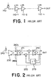
- the first conventional optical receiver for a burst signal comprises a photo diode 140 and a plurality of limit amplifier circuits 110-1, 110-2, 110-3, ..., 110-n connected in series to one one another.
- Each limit amplifier circuit has an offset compensating function determined by an offset compensation time constant of the such an offset compensation time constant is set to a predetermined value in each of the limit amplifier circuits.
- the offset compensation time constants of the limit amplifier circuits 110-1, 110-2, 110-3, ..., 110-n are give by ⁇ (1), ⁇ (2), ⁇ (3), ..., ⁇ (n), respectively.
- the offset compensation time constants in the limit amplifier circuits are very small in consideration of so as receive continuation of a predetermined bits having the same polarity.
- the second conventional optical receiver responding to a continuous signal only is structured by a photo diode 240, a preamplifier 230 of a differential type, and a post amplifier 270.
- a pair of outputs of the preamplifier 230 is led to the post-amplifier 270 through coupling capacitors 280a and 280b.
- each of the coupling capacitors 280a and 280b serves to carry out unipolar-to-bipolar transformation.
- the post-amplifier 270 comprises limit amplifier circuits 271 and 272 connected in series to each other through subtracters (unnumbered).
- the post-amplifier 270 compensates an internal offset thereof by having a negative feedback circuit which includes an integrating circuit 273.
- the integrating circuit 273 is operable to maintain a time average value of positive and negative outputs at a constant value.
- a PON (Passive Optical Network) system is well known as an optical subscriber system which is able to economically realize a narrow band service such as a telephone service. Recently, the PON system is enable to adapted in a field of optical communication. Furthermore, a single star system is also known as an effective method which realizes a wide band system by the use of existing resources utilized in the PON system. The single star system is described in 1995 IEICE Technical Report SSE95-140.
- the PON system is upgraded stepwise into the single star system.
- the existing resources of the PON system are used in common to the single star system.
- a system which comprises both the PON and the single star systems is existent before the completion of a complete single star system.
- ONU Optical Network Unit
- both types of the optical receivers are preferably small in size and inexpensive in cost.
- the optical receiver for the burst signal generally can also be used to receive the continuous signal.
- threshold control of received signal has been degraded in accuracy in comparison with the optical receiver designed to receive the continuous signal alone. This brings about a reduction of receiver sensitivity of the continuous signal.
- the optical receiver for the burst signal is small in the offset compensation time constant and large in a detecting error of an offset detector, such as a peak detecting circuit.
- the optical receiver is susceptible to an influence of an electromagnetic interference.
- the conventional optical receiver illustrated in Fig. 1 compensates an internal offset thereof by connecting, in series, a plurality of limit amplifier circuits having offset compensating function in order to accomplish a quick response.
- the multichannel optical link has a possibility that is applied to the technical field, such as an interconnection or a LAN (a Local Area Network).
- the optical receiver should have both two properties different from each other.
- One of the properties is to have a middle speed response to the burst signal together with wide phase margin necessary for signal decision.
- Another property is to have a very high speed response to the continuous signal and relatively high sensitivity.
- the optical receiver in the field should be small in size and low in cost.
- optical receiver illustrated in Fig. 1 and the optical receiver illustrated in Fig. 2 are completely different in structure from each other. Therefore, one of the two optical receivers illustrated in Figs. 1 and 2 cannot replaced by each other by only changing parts of their components.
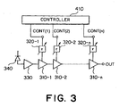
- an optical receiver is supplied with an input optical signal.
- the optical receiver comprises a photo diode 340 as a photoelectric transducer for transducing the input optical signal into an electrical signal, a preamplifier 330 for amplifying the electrical signal produced from the photo diode 340 into a preamplified electrical signal, and a plurality of limit amplifier circuits 310-1, 310-2, ..., and 310-n which are connected in series to one another and which have offset compensation functions,where n is a natural number greater than unity.
- the limit amplifier circuits 310-1 to 310-n successively amplify the preamplified electrical signal supplied from the preamplifier 330 to produce an amplified electrical signal through an output terminal OUT.
- the optical receiver further comprises a plurality of adjusting circuits 320-1, 320-2, ..., and 320-n connected to the plurality of limit amplifier circuits 310-1 to 310-n, respectively.
- Each of adjusting circuits 320-1 to 320-n serves to adjust an offset compensation time constant in each of the limit amplifier circuits 310-1 to 310-n.
- the plurality of the adjusting circuits 320-1 to 320-n may collectively be called an adjusting unit.
- the adjusting circuits 320-1, 320-2, ..., and 320-n have control ports CONT(1), CONT(2), ..., and CONT(n), respectively, which are connected to a controller 410.
- the offset compensation time constant in each of the limit amplifier circuits 310-1 to 310-n is changed by a control signal supplied from the controller 410 to each of the control ports CONT(1) to CONT(n).
- each of the offset compensation time constants is set to a small value so as to receive the burst signal and to realize a high speed response.
- each of the offset compensation time constants is set to a large value so as to receive the continuous signal which should be received with high sensitivity.
- the optical receiver can carry out the offset compensation with high accuracy and therefore has high sensitivity.
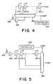
- an optical receiver is also supplied with an input optical signal like in the first embodiment.
- the optical receiver is similar to that illustrated in Fig. 3 except that an analog switch unit 350 is used as a selecting unit in place of the plurality of adjusting circuits 320-1 to 320-n illustrated in Fig. 3.
- the limit amplifier circuits 310-1 to 310-n has connection stages equal to in number to n.
- the limit amplifier circuits 310-1 to 310-n may collectively be called an n-stage limit amplifier circuit.
- the analog switch unit 350 is operable to change the number of the connection stages from on to another.
- the analog switch unit 350 which has a single input port supplied from the preamplifier 330 with the preamplified electrical signal and a plurality of output ports, n in number, selectively supplied with the preamplified electrical signal to send the same to one of the limit amplifier circuits 310-1 to 310-n in response to a control signal supplied from a controller 420 through a control port CONT.
- each of the limit amplifier circuits 310-1 to 310-n is implemented by a differential amplifier.
- the analog switch unit 350 supplies differential output signals, namely, a pair of output signals to each limit amplifier circuit 310-1 to 310-n. If each of the limit amplifier circuits 310-1 to 310-n is structured by an amplifier operable in response to a single input signal instead of the differential amplifier, the analog switch unit 350 may produce a single output signal.
- the limit amplifier circuits 310-1, 310-2, ..., and 310-n have offset compensation time constants ⁇ (1), ⁇ (2), ..., and ⁇ (n),respectively.
- a relationship between two adjacent one of the offset compensation time constants is defined by the following inequality represented by: ⁇ (j) > ⁇ (j+1), where j represents a positive integer smaller than n.
- the analog switch unit 350 carries out the selecting operation so that the preamplified electrical signal is supplied to one of the limit amplifier circuits 310-1 to 310-n that may be arranged relatively rearwards of the connection stages in the vicinity of the output terminals OUT.
- the optical receiver has the offset compensation time constant of a small value and is formed by a small number of the connection stages. For example, when the preamplified electrical signal is assumed to be supplied to the limit amplifier circuit 310-(n-1), the number of the connection stages becomes equal to two. In this event, the preamplified electrical signal is amplified by both the limit amplifier circuits 310-(n-1) and 310-n. As a result, the optical receiver is operable at a high speed and serves an optical receiver for the burst signal.
- the analog switch unit 350 should carry out the selecting operation so that the preamplified electrical signal is supplied to relatively forward one of the limit amplifier circuits 310-1 to 310-n that may be arranged relatively forwards of the connection stages.
- the preamplified electrical signal which is delivered through the analog switch unit 350 is amplified through a large number of the limit amplifier circuits.
- the optical receiver has the offset compensation time constant of a large value and the large number of the connection stages. For example, when the preamplified electrical signal is supplied to the limit amplifier circuit 310-2, the number of the connection stage becomes equal to (n-1). In this event, the preamplified electrical signal is amplified by the limit amplifier circuits 310-2 to 310-n. As a result, the optical receiver can compensate the offset with high accuracy.
- an optical receiver is similar to that illustrated in Fig. 4 except that an analog switch unit 360 is connected to output sides of the limit amplifier circuits 310-1 to 310-n connected in series to one another and is given output signals from the limit amplifier circuits 310-1 to 310-n.
- the analog switch unit 360 has a plurality of input ports connected to the output sides of the limit amplifier circuits 310-1 to 310-n, respectively. With this structure, the analog switch unit 360 selectively delivers one of the output signals of the limit amplifier circuits 310-1 to 310-n as the amplified electrical signal in response to a control signal supplied through a control port CONT sent from a controller 430.
- the analog switch unit 360 is given differential input signals (a pair of input signals) from each of the limit amplifier circuits 310-1 to 310-n because each limit amplifier circuit 310-1 to 310-n comprises the differential amplifier. If each of the limit amplifier circuits 310-1 to 310-n is structured by an amplifier which produces a single output signal, the analog switch unit 360 is operable in response to a single input signal.
- an analog switch circuit 360' is an example for explanation about the inner structure of the analog switch unit 360.
- the analog switch circuit 360' is an alternative type and comprises a differential amplifier 361 having transistors Tr611 and Tr612, a differential amplifier 362 having transistors Tr621 and Tr622, a differential amplifier 363 having transistors Tr631 and Tr632, and a driving current source 364.
- the analog switch circuit 360' can carry out the selecting operation for an analog signal having a frequency of several hundreds MHz and is operable at a high speed.
- the analog switch unit 360 can also carry out the selecting operation for the analog signal and is also operable at a high speed.
- the limit amplifier circuits 310-1, 310-2, ..., and 310-n have offset compensation time constants ⁇ (1), ⁇ (2), ..., and ⁇ (n), respectively.
- a relationship between two adjacent one of the the offset compensation time constants is defined by the following inequality represented by: ⁇ (j) > ⁇ (j + 1), where j represents a positive integer smaller than n.
- the optical receiver is used for receiving the burst signal.
- the analog switch unit 360 should select the output signal that is produced from the relatively forward one of the limit amplifier circuits 310-1 to 310-n.
- the selecting unit 360 selects the output signal of the limit amplifier circuit 310-2
- the output signal amplified by each of the limit amplifier circuits 310-1 and 310-2 is delivered through the output terminal OUT as the amplified electrical signal.
- the optical receiver has the offset compensation time constant of a small value and has the small number of the connection stages. As a result, the optical receiver enables a high speed response.
- the analog switch unit 360 should select the output signal of the limit amplifier circuits 310-1 to 310-n that is produced from a relatively rearward one of the limit amplifier circuits 310-1 to 310-n. For example, when the selecting unit 360 selects the output signal of the limit amplifier circuit 310-(n-1), each output signal amplified by the limit amplifier circuits 310-1 to 310-(n-1) is delivered through the output terminal OUT as the amplified electrical signal. According to the selecting operation, the preamplified electrical signal is amplified through the large number of the limit amplifier circuits. In this case, the optical receiver has the offset compensation time constant of a large value and the large number of the connection stages. As a result, the optical receiver can compensate the offset with high accuracy.
- an optical receiver according to a fourth embodiment of this invention is a combination of the first and the second embodiments described in conjunction with Figs. 3 and 4.
- the optical receiver has the adjusting function of the offset compensation time constant and the switching function of the number of the connection stages formed by the limit amplifier circuits 310-1 to 310-n.
- an optical receiver according to a fifth embodiment of this invention is a combination of the first and the third embodiments described in conjunction with Figs. 3 and 5.
- the optical receiver has the adjusting function of the offset compensation time constant and the switching function of the number of the connection stages of the limit amplifier circuits 310-1 to 310-n.
- an optical receiver is similar in structure to those illustrated in connection with the first through the fifth embodiments except that the optical receiver is implemented by a semiconductor integrated circuit.
- the optical receiver according to the sixth embodiment is illustrated in Fig. 9 and is substantially equivalent to the first embodiment and has an adjusting circuit 320' representative of each of adjusting circuit 320-1 to 320-n formed by the semiconductor integrated circuit. More specifically, the adjusting circuit 320' is formed by wiring patterns which can change connections from one to another.
- the offset compensation time constant of a single limit amplifier circuit 310 representative of each of the limit amplifier circuits 310-1 to 310-n is adjusted by changing the connections of the wiring patterns between terminals a1, a2, a3, ..., and ax coupled to capacitors C1, C2, C3, ..., and Cx and terminals b1, b2, b3, ..., and bx coupled to the single limit amplifier circuit 310, respectively.
- the selecting circuit 350' is implemented by the semiconductor integrated circuit including wiring patterns.
- one of the the limit amplifier circuits 310-1 to 310-n is selected by changing of connection of wiring patterns of the selecting circuit 350' between terminals b1, b2, ..., and bn coupled to the preamplifier 330 and terminals a1, a2, ..., and an coupled to the limit amplifier circuits 310-1 to 310-n.
- a selecting circuit 360'' formed by wiring patterns.
- one of the limit amplifier circuits 310-1 to 310-n is selected by changing of connections of the wiring patterns of the selecting circuit 360'' between terminals a1, a2, ..., and an coupled to the limit amplifier circuits 310-1 to 310-n and terminals b1, b2, ..., and bn coupled to the output terminal OUT.
- At least one of the adjusting circuit and the selecting circuit may be formed by wiring patterns which can change connections from one to another.
- the offset compensation time constant is uniquely determined in the sixth embodiment.
- An optical receiver is similar in structure to that illustrated in Figs. 3, 5, and 8 except that no adjusting circuits 320-1 to 320-n are included in the optical receiver and, instead, at least one of the limit amplifier circuits themselves has offset compensation functions determined by controllable offset compensation time constants.
- Such a controllable limit amplifier circuits amplifies the electrical signal into an amplified and controlled electrical signal in dependency upon the controllable offset compensation time constant.
- controllable limit amplifier circuit is specified by a single limit amplifier circuit 310' (suffixes omitted).
- controllable limit amplifier circuit 310' comprises a differential amplifier 311, two peak detecting circuits 312a and 312b, and two adders (unnumbered).
- Each of the peak detecting circuits 312a and 312b comprises a peak hold capacitor (not shown) for holding a peak value.
- the offset compensation time constant in the controllable limit amplifier circuit 310' is adjusted in dependency upon a capacitance of the peak hold capacitor.
- the offset compensation time constant of the controllable limit amplifier circuit can be controlled by adjusting the capacitance in each circuit.
- the above-mentioned capacitor in each limit amplifier circuit serves to adjust the offset compensation time constant.
- This structure dispenses with the adjusting circuits 320-1 to 320-n, as illustrated in Fig. 3, 5, and 8.
Landscapes
- Physics & Mathematics (AREA)
- Electromagnetism (AREA)
- Engineering & Computer Science (AREA)
- Computer Networks & Wireless Communication (AREA)
- Signal Processing (AREA)
- Optical Communication System (AREA)
- Amplifiers (AREA)
- Cable Transmission Systems, Equalization Of Radio And Reduction Of Echo (AREA)
Claims (24)
- Optischer Empfänger, welcher ansprechend auf ein optisches Eingangssignal betriebsfähig ist, um ein elektrisches Ausgangssignal zu erzeugen, wobei der optische Signalempfänger Folgendes aufweist:dadurch gekennzeichnet, dass der optische Signalempfänger weiter Folgendes aufweist:einen photoelektrischen Messwandler (340) zum Umwandeln des optischen Eingangssignals in ein elektrisches Signal;Grenzwert-Verstärkerschaltkreise (310-1, 310-2,..., und 310-n), welche in Reihe geschaltet sind und Offset-Kompensationsfunktionen aufweisen, die jeweils durch Offset-Kompensations-Zeitkonstanten festgelegt sind, wobei die Grenzwert-Verstärkerschaltkreise das elektrische Signal zur Erzeugung eines verstärkten elektrischen Signals verstärken; undAusgabevorrichtungen (OUT) zur Erzeugung des verstärkten elektrischen Signals als das elektrische Ausgangssignal,Einstellvorrichtungen (320, 320', 350, 350', und/oder 360, 360' 360''), welche mit den Grenzwert-Verstärkerschaltkreisen (310-1, 310-2, ..., und 310-n) zum Einstellen mindestens einer der Offset-Kompensations-Zeitkonstanten verbunden ist, um die Grenzwert-Verstärkerschaltkreise zu veranlassen, das verstärkte elektrische Signal zu erzeugen.
- Optischer Empfänger nach Anspruch 1, dadurch gekennzeichnet, dass er Folgendes aufweist:als die Grenzwert-Verstärkerschaltkreise eine Vielzahl von Grenzwert-Verstärkerschaltkreisen (310-1, 310-2,..., und 310-n), die in Reihe geschaltet sind und Offset-Kompensationsfunktionen aufweisen, die jeweils durch steuerbare Offset-Kompensations-Zeitkonstanten bestimmt sind, wobei die Vielzahl von Grenzwert-Verstärkerschaltkreisen (310-1, 310-2,..., und 310-n) das elektrische Signal zur Erzeugung eines verstärkten und gesteuerten elektrischen Signals in Abhängigkeit von den gesteuerten Offset-Kompensations-Zeitkonstanten verstärken;als die Einstellvorrichtungen Einstellvorrichtungen (320, 320'), die mit der Vielzahl von Grenzwert-Verstärkerschaltkreisen (310-1, 310-2,...,310-n) zum Einstellen mindestens einer der Offset-Kompensations-Zeitkonstanten verbunden ist, um die Grenzwert-Verstärkerschaltkreise (310-1, 310-2,..., und 310-n) zu veranlassen, das verstärkte und gesteuerte elektrische Signal zu erzeugen; undals die Ausgabevorrichtung eine Ausgabevorrichtung (OUT) zum Erzeugen des verstärkten und gesteuerten Signals als das elektrische Ausgangssignal.
- Optischer Empfänger nach Anspruch 2, dadurch gekennzeichnet, dass die Einstellvorrichtung (320) Folgendes aufweist:eine Vielzahl von Einstellschaltkreisen (320-1, 320-2, ..., und 320-n), die jeweils mit den Grenzwert-Verstärkerschaltkreisen zur Einstellung der Offset-Kompensations-Zeitkonstanten der Grenzwert-Verstärkerschaltkreise (310-1, 310-2, ..., und 310-n) verbunden sind.
- Optischer Empfänger nach Anspruch 3, dadurch gekennzeichnet dass:jeder der Einstellschaltkreise (320-1, 320-2, ..., und 320-n) eine steuerbare Zeitkonstante aufweist, die zur Bestimmung einer jeden Offset-Kompensations-Zeitkonstanten in jedem der Grenzwert-Verstärkerschaltkreise (310-1, 310-2, ..., und 310-n) dient.
- Optischer Empfänger nach Anspruch 4, dadurch gekennzeichnet, dass die Einstellvorrichtung Folgendes aufweist:eine Steuervorrichtung (410) zur Lieferung eines Steuersignals an jeden der Einstellschaltkreise (320-1, 320-2, ..., und 320-n) zum Steuern der steuerbaren Zeitkonstanten in jedem Einstellschaltkreis.
- Optischer Empfänger nach Anspruch 2, dadurch gekennzeichnet, dass jeder der Grenzwert-Verstärkerschaltkreise (310-1, 310-2, ..., und 310-n) einen Höchstwert-Erfassungsschaltkreis zum Halten eines Höchstwerts sowie einen mit dem Höchstwert-Erfassungsschaltkreis verbundenen Differenzverstärker aufweist.
- Optischer Empfänger nach Anspruch 2, dadurch gekennzeichnet, dass der optische Empfänger als integrierter Halbleiterschaltkreis realisiert ist, wobei die Einstellvorrichtung (320') durch Verdrahtungsmuster gebildet ist.
- Optischer Empfänger nach Anspruch 1, dadurch gekennzeichnet, dass er Folgendes aufweist:als die Grenzwert-Verstärkerschaltkreise erste bis einschließlich n-te Grenzwert-Verstärkerschaltkreise (310-1, 310-2, ..., und 310-n), welche zur Bildung erster bis einschließlich n-ter Verbindungsstufen jeweils in Reihe geschaltet sind, und welche Offset-Kompensationsfunktionen aufweisen, die durch Offset-Kompensations-Zeitkonstanten bestimmt sind, wobei die ersten bis einschließlich n-ten Grenzwert-Verstärkerschaltkreise das an einen der ersten bis einschließlich n-ten Verstärkerschaltkreise zur Erzeugung eines verstärkten elektrischen Signals mit Hilfe der n-ten Grenzwert-Verstärkerschaltkreise gelieferte elektrische Signal verstärken;als die Einstellvorrichtung Auswahlvorrichtungen (350, 350'), an welche das elektrische Signal geliefert wird und welche mit den ersten bis einschließlich den n-ten Grenzwert-Verstärkerschaltkreisen (310-1, 310-2, ..., und 310-n) zur Auswahl eines der ersten bis einschließlich der n-ten Grenzwert-Verstärkerschaltkreise als ausgewählter Grenzwert-Verstärkerschaltkreis verbunden sind, um die Anzahl der Grenzwert-Verstärkerschaltkreise zwischen dem ausgewählten Grenzwert-Verstärkerschaltkreis und dem n-ten Grenzwert-Verstärkerschaltkreis zu ändern, und als die Ausgabevorrichtung, um das elektrische Signal an den ausgewählten Grenzwert-Verstärkerschaltkreis zu liefern; undals die Ausgabevorrichtung eine Ausgabevorrichtung (OUT) zum Liefern des elektrischen Ausgangssignals von dem n-ten Grenzwert-Verstärkerschaltkreis durch Verstärken des elektrischen Signals zwischen dem ausgewählten Grenzwert-Verstärkerschaltkreis und dem n-ten Grenzwert-Verstärkerschaltkreis.
- Optischer Empfänger nach Anspruch 8, dadurch gekennzeichnet, dass jeder erste bis einschließlich dem n-ten Grenzwert-Verstärkerschaltkreis (310-1, 310-2, ..., 310-n) Eingangs- und Ausgangsanschlüsse aufweist;wobei die Auswahlvorrichtung mit den Eingangsanschlüssen des ersten bis einschließlich des n-ten Grenzwert-Verstärkerschaltkreises (310-1, 310-2, ..., und 310-n) verbunden ist.
- Optischer Empfänger nach Anspruch 8, dadurch gekennzeichnet, dass die Auswahlvorrichtung Folgendes aufweist:einen Analogschalter, welcher einen Eingangsanschluss und erste bis einschließlich n-te Ausgangsanschlüsse aufweist, und der den Eingangsanschluss mit einem ausgewählten aus den ersten bis einschließlich den n-ten Ausgangsanschlüssen verbindet, um das elektrische Signal vom Eingangsanschluss an den ausgewählten Grenzwert-Verstärkerschaltkreis zu liefern.
- Optischer Empfänger nach Anspruch 10, dadurch gekennzeichnet, dass die Auswahlvorrichtung eine Steuereinrichtung (420) zum Liefern eines Steuersignals an den Analogschalter aufweist, um eine Verbindung und eine Signallieferung darin zu steuern.
- Optischer Empfänger nach Anspruch 8, dadurch gekennzeichnet, dass jeder der ersten bis einschließlich der n-ten Grenzwert-Verstärkerschaltkreise (310-1, 310-2, ..., und 310-n) einen Höchstwert-Erfassungsschaltkreis zum Halten eines Höchstwerts sowie einen mit dem Höchstwert-Erfassungsschaltkreis verbundenen Differenzverstärker aufweist.
- Optischer Empfänger nach Anspruch 8, dadurch gekennzeichnet, dass der optische Empfänger als integrierter Halbleiterschaltkreis realisiert ist, wobei die Auswahlvorrichtung (350') mit Hilfe von Verdrahtungsmustern gebildet ist.
- Optischer Empfänger nach Anspruch 1, dadurch gekennzeichnet, dass der optische Empfänger Folgendes aufweist:als Grenzwert-Verstärkerschaltkreise erste bis einschließlich n-te Grenzwert-Verstärkerschaltkreise (310-1, 310-2, ..., und 310-n), die zur Bildung erster bis einschließlich n-ter Verbindungsstufen jeweils in Reihe geschaltet sind, und welche durch Offset-Kompensations-Zeitkonstanten festgelegte Offset-Kompensationsfunktionen aufweisen, wobei die ersten bis einschließlich die n-ten Grenzwert-Verstärkerschaltkreise (310-1, 310-2, ..., und 310-n) das an den ersten Grenzwert-Verstärkerschaltkreis gelieferte elektrische Signal verstärken, um ein verstärktes elektrisches Signal mit Hilfe eines der ersten bis einschließlich der n-ten Grenzwert-Verstärkerschaltkreise (310-1, 310-2, ..., und 310-n) zu erzeugen;als die Einstellvorrichtung Auswahlvorrichtungen (360, 360', 360''), welche mit den ersten bis einschließlich den n-ten Grenzwert-Verstärkerschaltkreisen (310-1, 310-2, ..., und 310-n) zur Auswahl eines der ersten bis einschließlich der n-ten Grenzwert-Verstärkerschaltkreise als ausgewählter Grenzwert-Verstärkerschaltkreis verbunden sind, um die Anzahl der Grenzwert-Verstärkerschaltkreise zwischen dem ersten Grenzwert-Verstärkerschaltkreis und dem ausgewählten Grenzwert-Verstärkerschaltkreis zu ändern, und um das verstärkte elektrische Signal vom ausgewählten Grenzwert-Verstärkerschaltkreis zu liefern; undals die Ausgabevorrichtung eine Ausgabevorrichtung (OUT) zum Liefern des elektrischen Ausgangssignals vom ausgewählten Grenzwert-Verstärkerschaltkreis durch Verstärken des elektrischen Signals zwischen dem ersten Grenzwert-Verstärkerschaltkreis und dem ausgewählten Grenzwert-Verstärkerschaltkreis.
- Optischer Empfänger nach Anspruch 14, dadurch gekenzeichnet, dass jeder der ersten bis einschließlich der n-ten Grenzwert-Verstärkerschaltkreise (310-1, 310-2, ..., und 310-n) Eingangs- und Ausgangsanschlüsse aufweist;wobei die Auswahlvorrichtung mit den Ausgangsanschlüssen der ersten bis einschließlich der n-ten Grenzwert-Verstärkerschaltkreise (310-1, 310-2, ..., und 310-n) verbunden ist.
- Optischer Empfänger nach Anspruch 15, dadurch gekennzeichnet, dass die Auswahlvorrichtung Folgendes aufweist:einen Analogschalter, der erste bis einschließlich n-te Eingangsanschlüsse sowie einen Ausgangsanschluss aufweist, und der einen ausgewählten aus den ersten bis einschließlich den n-ten Eingangsanschlüssen mit dem Ausgangsanschluss verbindet, um das elektrische Signal vom ausgewählten Grenzwert-Verstärkerschaltkreis an den Ausgangsanschluss zu liefern.
- Optischer Empfänger nach Anspruch 16, dadurch gekennzeichnet, dass die Auswahlvorrichtung eine Steuervorrichtung (430) zum Liefern eines Steuersignals an den Analogschalter aufweist, um eine Verbindung und eine Signallieferung darin zu steuern.
- Optischer Empfänger nach Anspruch 14, dadurch gekennzeichnet; dass jeder der ersten bis einschließlich der n-ten Grenzwert-Verstärkerschaltkreise (310-1, 310-2, ..., und 310-n) einen Höchstwert-Erfassungsschaltkreis zum Halten eines Höchstwerts sowie einen mit dem Höchstwert-Erfassungsschaltkreis verbundenen Differenzverstärker aufweist.
- Optischer Empfänger nach Anspruch 14, dadurch gekennzeichnet, dass der optische Empfänger als integrierter Halbleiterschaltkreis realisiert ist, wobei die Auswahlvorrich-tung (360'') mit Hilfe von Verdrahtungsmustern gebildet ist.
- Optischer Empfänger nach Anspruch 1, dadurch gekennzeichnet, dass der optische Empfänger Folgendes aufweist:als Grenzwert-Verstärkerschaltkreise erste bis einschließlich n-te Grenzwert-Verstärkerschaltkreise (310-1, 310-2, ..., und 310-n), die zur Bildung erster bis einschließlich n-ter Verbindungsstufen jeweils in Reihe geschaltet sind, und welche durch steuerbare Offset-Kompensations-Zeitkonstanten festgelegte Offset-Kompensationsfunktionen aufweisen, wobei der erste bis einschließlich der n-te Grenzwert-Verstärkerschaltkreis (310-1, 310-2, ..., und 310-n) das an einen der ersten bis einschließlich der n-ten Grenzwert-Verstärkerschaltkreise gelieferte elektrische Signal verstärken, um ein verstärktes und gesteuertes elektrisches Signal mit Hilfe des n-ten Grenzwert-Verstärkerschaltkreises in Abhängigkeit von den gesteuerten Offset-Kompensations-Zeitkonstanten zu erzeugen;als eine der Einstellvorrichtungen eine Einstellvorrichtung (320), die mit den ersten bis einschließlich den n-ten Grenzwert-Verstärkerschaltkreisen (310-1, 310-2, ..., und 310-n) zum Einstellen mindestens einer der Offset-Kompensations-Zeitkonstanten verbunden ist, um die Grenzwert-Verstärkerschaltkreise zu veranlassen, das verstärkte und gesteuerte elektrische Signal zu erzeugen;als die andere der Einstellvorrichtungen eine Auswahlvorrichtung (350), an welche das elektrische Signal geliefert wird und welche mit den ersten bis einschließlich den n-ten Grenzwert-Verstärkerschaltkreisen (310-1, 310-2, ..., und 310-n) zum Auswählen eines Grenzwert-Verstärkerschaltkreises aus den ersten bis einschließlich den n-ten Grenzwert-Verstärkerschaltkreisen als ausgewählter Grenzwert-Verstärkerschaltkreis verbunden ist, um die Anzahl der Grenzwert-Verstärkerschaltkreise zwischen dem ausgewählten Grenzwert-Verstärkerschaltkreis und dem n-ten Grenzwert-Verstärkerschaltkreis zu ändern und um das elektrische Signal an den ausgewählten Grenzwert-Verstärkerschaltkreis zu liefern; undals Ausgabevorrichtung eine Ausgabevorrichtung (OUT) zum Liefern des elektrischen Ausgangssignals vom n-ten Grenzwert-Verstärkerschaltkreis durch Verstärken und Einstellen des elektrischen Signals zwischen dem ausgewählten Grenzwert-Verstärkerschaltkreis und dem n-ten Grenzwert-Verstärkerschaltkreis.
- Optischer Empfänger nach Anspruch 1, dadurch gekennzeichnet, dass der optische Empfänger Folgendes aufweist:als die Grenzwert-Verstärkerschaltkreise erste bis einschließlich n-te Grenzwert-Verstärkerschaltkreise (310-1, 310-2, ..., und 310-n), die zur Bildung erster bis einschließlich n-ter Verbindungsstufen jeweils in Reihe geschaltet sind, und welche durch steuerbare Offset-Kompensations-Zeitkonstanten festgelegte Offset-Kompensationsfunktionen aufweisen, wobei die ersten bis einschließlich die n-ten Grenzwert-Verstärkerschaltkreise (310-1, 310-2, ..., und 310-n) das an den ersten Grenzwert-Verstärkerschaltkreis gelieferte elektrische Signal verstärken, um ein verstärktes und gesteuertes elektrisches Signal mit Hilfe eines Grenzwert-Verstärkerschaltkreises aus den ersten bis einschließlich den n-ten Grenzwert-Verstärkerschaltkreisen (310-1, 310-2, ..., und 310-n) in Abhängigkeit von den gesteuerten Offset-Kompensations-Zeitkonstanten zu erzeugen;als eine der Einstellvorrichtungen eine Einstellvorrichtung (320), die mit den ersten bis einschließlich den n-ten Grenzwert-Verstärkerschaltkreisen (310-1, 310-2, ..., und 310-n) zum Einstellen mindestens einer der Offset-Kompensations-Zeitkonstanten verbunden ist, um die Grenzwert-Verstärkerschaltkreise zu veranlassen, das verstärkte und gesteuerte elektrische Signal zu erzeugen;als die andere der Einstellvorrichtungen eine Auswahlvorrichtung (360), welche mit den ersten bis einschließlich den n-ten Grenzwert-Verstärkerschaltkreisen (310-1, 310-2, ..., und 310-n) zum Auswählen eines Grenzwert-Verstärkerschaltkreises aus den ersten bis einschließlich den n-ten Grenzwert-Verstärkerschaltkreisen (310-1, 310-2, ..., und 310-n) als ausgewählter Grenzwert-Verstärkerschaltkreis verbunden ist, um die Anzahl der Grenzwert-Verstärkerschaltkreise zwischen dem ersten Grenzwert-Verstärkerschaltkreis und dem ausgewählten Grenzwert-Verstärkerschaltkreis zu ändern, und um das verstärkte und gesteuerte elektrische Signal vom ausgewählten Grenzwert-Verstärkerschaltkreis zu liefern; undals Ausgabevorrichtung eine Ausgabevorrichtung (OUT) zum Liefern des elektrischen Ausgangssignals von dem ausgewählten Grenzwert-Verstärkerschaltkreis durch Verstärken und Einstellen des elektrischen Signals zwischen dem ersten Grenzwert-Verstärkerschaltkreis und dem ausgewählten Grenzwert-Verstärkerschaltkreis.
- Optischer Empfänger nach Anspruch 1, dadurch gekennzeichnet, dass mindestens einer der Grenzwert-Verstärkerschaltkreise steuerbar ist, wobei die Vielzahl der Grenzwert-Verstärkerschaltkreise das elektrische Signal zur Erzeugung eines verstärkten und gesteuerten elektrischen Signals in Abhängigkeit von den gesteuerten Offset-Kompensations-Zeitkonstanten verstärkt.
- Optischer Empfänger nach Anspruch 22, dadurch gekennzeichnet, dass jeder Grenzwert-Verstärkerschaltkreis einen Höchstwert-Erfassungsschaltkreis (312a, 312b) zum Halten eines Höchstwerts sowie einen mit dem Höchstwert-Erfassungsschaltkreis verbundenen Differenzverstärker aufweist;wobei der Höchstwert-Erfassungsschaltkreis die steuerbare Offset-Kompensations-Zeitkonstante aufweist.
- Optischer Empfänger nach Anspruch 23, dadurch gekennzeichnet, dass der Höchstwert-Erfassungsschaltkreis einen Kondensator zum Bestimmen der steuerbaren Offset-Kompensations-Zeitkonstanten aufweist.
Applications Claiming Priority (3)
| Application Number | Priority Date | Filing Date | Title |
|---|---|---|---|
| JP27670096 | 1996-10-18 | ||
| JP8276700A JPH10126351A (ja) | 1996-10-18 | 1996-10-18 | 光受信回路 |
| JP276700/96 | 1996-10-18 |
Publications (3)
| Publication Number | Publication Date |
|---|---|
| EP0837570A2 EP0837570A2 (de) | 1998-04-22 |
| EP0837570A3 EP0837570A3 (de) | 2002-06-12 |
| EP0837570B1 true EP0837570B1 (de) | 2005-01-26 |
Family
ID=17573116
Family Applications (1)
| Application Number | Title | Priority Date | Filing Date |
|---|---|---|---|
| EP97118090A Expired - Lifetime EP0837570B1 (de) | 1996-10-18 | 1997-10-17 | Optischer Empfänger für Burst und kontinuierliche Signale |
Country Status (4)
| Country | Link |
|---|---|
| US (1) | US6081362A (de) |
| EP (1) | EP0837570B1 (de) |
| JP (1) | JPH10126351A (de) |
| DE (1) | DE69732332D1 (de) |
Families Citing this family (22)
| Publication number | Priority date | Publication date | Assignee | Title |
|---|---|---|---|---|
| SE506200C2 (sv) * | 1996-03-25 | 1997-11-17 | Ericsson Telefon Ab L M | Anordning och förfarande för kompensering av offsetspänningar vid mottagning av optiska signaler |
| KR100331105B1 (ko) * | 2000-03-11 | 2002-04-06 | 신현국 | I²c 통신 프로토콜의 전기통신 인터페이스 모듈에연결되는 광통신 인터페이스 모듈 |
| JP2003168933A (ja) * | 2001-11-30 | 2003-06-13 | Nef:Kk | 光受信回路 |
| KR100445910B1 (ko) * | 2001-12-27 | 2004-08-25 | 한국전자통신연구원 | 광신호 세기의 변동에 관계없이 최적의 수신 성능을 갖는광신호 수신장치 및 그 방법 |
| JP3880906B2 (ja) * | 2002-08-22 | 2007-02-14 | 富士通株式会社 | 波形劣化補償機能を有する受信装置 |
| US6917233B1 (en) | 2002-09-11 | 2005-07-12 | Koninklijke Philips Electronics N.V. | Limiting amplifier and method for amplifying an input signal |
| KR100467323B1 (ko) * | 2002-09-23 | 2005-01-24 | 한국전자통신연구원 | 광 수신기 출력 신호의 판별 수준 최적화 방법 및 장치 |
| KR100462407B1 (ko) * | 2002-11-07 | 2004-12-17 | 한국전자통신연구원 | 순방향 오류 정정(fec)을 이용한 광수신기의 출력최적화 방법 및 이를 이용한 광수신 시스템 |
| KR100537901B1 (ko) * | 2003-03-29 | 2005-12-20 | 한국전자통신연구원 | 버스트 모드 광 수신기 |
| KR100535311B1 (ko) * | 2003-12-18 | 2005-12-09 | 한국전자통신연구원 | 광 수신기의 문턱전압 제어 장치 |
| US7499648B2 (en) * | 2004-09-27 | 2009-03-03 | Mindspeed Technologies, Inc. | Multistage amplifier for rapid acquisition and random received signal power applications |
| US8509629B2 (en) * | 2007-10-26 | 2013-08-13 | Mindspeed Technologies, Inc. | High sensitivity two-stage amplifier |
| JP4691128B2 (ja) * | 2008-03-28 | 2011-06-01 | 日本電信電話株式会社 | 増幅回路 |
| US10097908B2 (en) | 2014-12-31 | 2018-10-09 | Macom Technology Solutions Holdings, Inc. | DC-coupled laser driver with AC-coupled termination element |
| US10044328B2 (en) | 2015-07-20 | 2018-08-07 | Macom Technology Solutions Holdings, Inc. | Transimpedance amplifier with bandwidth extender |
| TWI750216B (zh) | 2016-08-30 | 2021-12-21 | 美商Macom技術方案控股公司 | 具分散式架構之驅動器 |
| US10630052B2 (en) | 2017-10-04 | 2020-04-21 | Macom Technology Solutions Holdings, Inc. | Efficiency improved driver for laser diode in optical communication |
| JP7653790B2 (ja) | 2018-05-30 | 2025-03-31 | メイコム テクノロジー ソリューションズ ホールディングス インコーポレイテッド | 集積回路に基づくac結合トポロジ |
| US11005573B2 (en) * | 2018-11-20 | 2021-05-11 | Macom Technology Solutions Holdings, Inc. | Optic signal receiver with dynamic control |
| US12013423B2 (en) | 2020-09-30 | 2024-06-18 | Macom Technology Solutions Holdings, Inc. | TIA bandwidth testing system and method |
| US11658630B2 (en) | 2020-12-04 | 2023-05-23 | Macom Technology Solutions Holdings, Inc. | Single servo loop controlling an automatic gain control and current sourcing mechanism |
| US12395130B2 (en) | 2022-12-27 | 2025-08-19 | Macom Technology Solutions Holdings, Inc. | Variable gain optical modulator with open collector driver amplifier and method of operation |
Family Cites Families (4)
| Publication number | Priority date | Publication date | Assignee | Title |
|---|---|---|---|---|
| US4257125A (en) * | 1979-05-01 | 1981-03-17 | The Singer Company | Receiver for unipolar Manchester fiber optics signals |
| US5475342A (en) * | 1993-04-19 | 1995-12-12 | Nippon Telegraph And Telephone Corporation | Amplifier for stably maintaining a constant output |
| JPH08223228A (ja) * | 1994-03-17 | 1996-08-30 | Fujitsu Ltd | 等化増幅器及びこれを用いた受信機並びにプリアンプ |
| JPH08279718A (ja) * | 1995-04-07 | 1996-10-22 | Nec Corp | オフセット除去増幅回路 |
-
1996
- 1996-10-18 JP JP8276700A patent/JPH10126351A/ja active Pending
-
1997
- 1997-10-17 DE DE69732332T patent/DE69732332D1/de not_active Expired - Lifetime
- 1997-10-17 US US08/951,603 patent/US6081362A/en not_active Expired - Fee Related
- 1997-10-17 EP EP97118090A patent/EP0837570B1/de not_active Expired - Lifetime
Also Published As
| Publication number | Publication date |
|---|---|
| US6081362A (en) | 2000-06-27 |
| DE69732332D1 (de) | 2005-03-03 |
| EP0837570A3 (de) | 2002-06-12 |
| JPH10126351A (ja) | 1998-05-15 |
| EP0837570A2 (de) | 1998-04-22 |
Similar Documents
| Publication | Publication Date | Title |
|---|---|---|
| EP0837570B1 (de) | Optischer Empfänger für Burst und kontinuierliche Signale | |
| US5256987A (en) | Power amplifier device having a plurality of power amplifier units connected in parallel | |
| US6122085A (en) | Lightwave transmission techniques | |
| US5892609A (en) | Digital signal receiver circuit | |
| US6366377B1 (en) | Optical network and switch control method for use in the optical network | |
| JP2002520890A (ja) | 改良型光ファイバ増幅器制御 | |
| JP4440343B2 (ja) | 光網 | |
| JP2005006313A (ja) | 受動光通信網の光パワー等化装置 | |
| US5267073A (en) | Amplifier adapter for optical lines | |
| US7105797B2 (en) | Optical receiving circuit | |
| US5745276A (en) | Universal optical signal receiver | |
| JP3226762B2 (ja) | データアクセス装置 | |
| US20050140454A1 (en) | Pre-amplifier for an optical communication | |
| US6819722B2 (en) | Offset control circuit, optical receiver using the same and optical communication system | |
| US6525858B1 (en) | Optical receiver and optical network system using thereof | |
| RU2248087C2 (ru) | Оптический усилитель и оптическая линия передачи | |
| US7304543B2 (en) | Burst-mode TIA (trans-impedance amplifier) | |
| JP3023705B2 (ja) | 予備チャンネル切替え装置および方法 | |
| US20070196105A1 (en) | Optical network unit and control method thereof | |
| US7356262B2 (en) | Time division multiplexing of analog signals in an optical transceiver | |
| EP1317084A3 (de) | Optische Verstärkeranordnung | |
| US20060127090A1 (en) | Apparatus and method for controlling gain of optical receiver in optical communication system | |
| US6169615B1 (en) | Wavelength division multiplex optical transmission apparatus | |
| US6292059B1 (en) | Systems, methods, and circuits for providing thermal compensation in amplifiers | |
| JP3642738B2 (ja) | 光パワーレベル等化回路 |
Legal Events
| Date | Code | Title | Description |
|---|---|---|---|
| PUAI | Public reference made under article 153(3) epc to a published international application that has entered the european phase |
Free format text: ORIGINAL CODE: 0009012 |
|
| AK | Designated contracting states |
Kind code of ref document: A2 Designated state(s): AT BE CH DE DK ES FI FR GB GR IE IT LI LU MC NL PT SE |
|
| AX | Request for extension of the european patent |
Free format text: AL;LT;LV;RO;SI |
|
| PUAL | Search report despatched |
Free format text: ORIGINAL CODE: 0009013 |
|
| AK | Designated contracting states |
Kind code of ref document: A3 Designated state(s): AT BE CH DE DK ES FI FR GB GR IE IT LI LU MC NL PT SE |
|
| AX | Request for extension of the european patent |
Free format text: AL;LT;LV;RO;SI |
|
| RIC1 | Information provided on ipc code assigned before grant |
Free format text: 7H 04B 10/158 A, 7H 03F 3/08 B |
|
| 17P | Request for examination filed |
Effective date: 20020501 |
|
| AKX | Designation fees paid |
Designated state(s): DE FR GB NL SE |
|
| 17Q | First examination report despatched |
Effective date: 20040112 |
|
| GRAP | Despatch of communication of intention to grant a patent |
Free format text: ORIGINAL CODE: EPIDOSNIGR1 |
|
| GRAS | Grant fee paid |
Free format text: ORIGINAL CODE: EPIDOSNIGR3 |
|
| GRAA | (expected) grant |
Free format text: ORIGINAL CODE: 0009210 |
|
| AK | Designated contracting states |
Kind code of ref document: B1 Designated state(s): DE FR GB NL SE |
|
| PG25 | Lapsed in a contracting state [announced via postgrant information from national office to epo] |
Ref country code: NL Free format text: LAPSE BECAUSE OF FAILURE TO SUBMIT A TRANSLATION OF THE DESCRIPTION OR TO PAY THE FEE WITHIN THE PRESCRIBED TIME-LIMIT Effective date: 20050126 Ref country code: FR Free format text: LAPSE BECAUSE OF FAILURE TO SUBMIT A TRANSLATION OF THE DESCRIPTION OR TO PAY THE FEE WITHIN THE PRESCRIBED TIME-LIMIT Effective date: 20050126 |
|
| REG | Reference to a national code |
Ref country code: GB Ref legal event code: FG4D |
|
| REG | Reference to a national code |
Ref country code: IE Ref legal event code: FG4D |
|
| REF | Corresponds to: |
Ref document number: 69732332 Country of ref document: DE Date of ref document: 20050303 Kind code of ref document: P |
|
| PG25 | Lapsed in a contracting state [announced via postgrant information from national office to epo] |
Ref country code: SE Free format text: LAPSE BECAUSE OF FAILURE TO SUBMIT A TRANSLATION OF THE DESCRIPTION OR TO PAY THE FEE WITHIN THE PRESCRIBED TIME-LIMIT Effective date: 20050426 |
|
| PG25 | Lapsed in a contracting state [announced via postgrant information from national office to epo] |
Ref country code: DE Free format text: LAPSE BECAUSE OF FAILURE TO SUBMIT A TRANSLATION OF THE DESCRIPTION OR TO PAY THE FEE WITHIN THE PRESCRIBED TIME-LIMIT Effective date: 20050427 |
|
| NLV1 | Nl: lapsed or annulled due to failure to fulfill the requirements of art. 29p and 29m of the patents act | ||
| PG25 | Lapsed in a contracting state [announced via postgrant information from national office to epo] |
Ref country code: GB Free format text: LAPSE BECAUSE OF NON-PAYMENT OF DUE FEES Effective date: 20051017 |
|
| PLBE | No opposition filed within time limit |
Free format text: ORIGINAL CODE: 0009261 |
|
| STAA | Information on the status of an ep patent application or granted ep patent |
Free format text: STATUS: NO OPPOSITION FILED WITHIN TIME LIMIT |
|
| 26N | No opposition filed |
Effective date: 20051027 |
|
| EN | Fr: translation not filed | ||
| GBPC | Gb: european patent ceased through non-payment of renewal fee |
Effective date: 20051017 |