EP0824225A2 - Ausrichtverfahren - Google Patents
Ausrichtverfahren Download PDFInfo
- Publication number
- EP0824225A2 EP0824225A2 EP97203250A EP97203250A EP0824225A2 EP 0824225 A2 EP0824225 A2 EP 0824225A2 EP 97203250 A EP97203250 A EP 97203250A EP 97203250 A EP97203250 A EP 97203250A EP 0824225 A2 EP0824225 A2 EP 0824225A2
- Authority
- EP
- European Patent Office
- Prior art keywords
- wafer
- mark
- mask
- surface area
- pattern
- Prior art date
- Legal status (The legal status is an assumption and is not a legal conclusion. Google has not performed a legal analysis and makes no representation as to the accuracy of the status listed.)
- Withdrawn
Links
Images


Classifications
-
- G—PHYSICS
- G03—PHOTOGRAPHY; CINEMATOGRAPHY; ANALOGOUS TECHNIQUES USING WAVES OTHER THAN OPTICAL WAVES; ELECTROGRAPHY; HOLOGRAPHY
- G03F—PHOTOMECHANICAL PRODUCTION OF TEXTURED OR PATTERNED SURFACES, e.g. FOR PRINTING, FOR PROCESSING OF SEMICONDUCTOR DEVICES; MATERIALS THEREFOR; ORIGINALS THEREFOR; APPARATUS SPECIALLY ADAPTED THEREFOR
- G03F9/00—Registration or positioning of originals, masks, frames, photographic sheets or textured or patterned surfaces, e.g. automatically
- G03F9/70—Registration or positioning of originals, masks, frames, photographic sheets or textured or patterned surfaces, e.g. automatically for microlithography
Definitions
- This invention relates to an alignment system and, more particularly, to an alignment system for use in a step-and-repeat type exposure apparatus, for detecting the relative position of an original such as a mask and a substrate such as a semiconductor wafer.
- the alignment and exposure system in conventional step-and-repeat type exposure apparatuses there are a global alignment method, a die-by-die alignment method and a zone alignment method.
- the global alignment method the alignment operation is effected only with respect to some of all the shot areas of one wafer by using alignment marks and, after this, exposures are effected while moving a wafer stage stepwise through a distance corresponding to the grid interval (the distance between the centers of adjacent shot areas).
- the alignment operation using alignment marks and the exposure operation are effected.
- the zone alignment method a single alignment operation is effected in relation to plural shot areas.
- the exposure of that shot area is given up or the exposure is effected after the wafer is moved from the preceding shot area position by a distance corresponding to the grid interval or, alternatively, the wafer is moved from the preceding shot area position to the grid point (the design center of the shot area) of the current shot area and thereafter a corrective drive is effected on the basis of the alignment correction quantity related to an adjacent alignment completed shot area.
- the precision is insufficient for attaining the linewidth of 0.25 micron order.
- a plurality of correction (quantitative calculation) processing sequences are provided and, in accordance with the number of the pieces of the mark measured information obtained at that shot area, one correction processing sequence is selected automatically.
- the term "alignment operation” means adjustment of the positional relationship between an original and a substrate to be exposed, by using marks provided on the original and/or the substrate.
- the direction of adjustment is not a matter.
- the position adjustment in a plane (X-Y plane) parallel to the surface of the substrate or the original will be referred to as “AA (autoalignment)”
- the position adjustment in a direction (Z-axis direction) perpendicular to the X-Y plane e.g. the proximity gap setting of the substrate and the original, or the focus adjustment
- AF autofocusing
- a correction processing sequence is selected.
- each shot area is equipped with spare marks and, if the number of the pieces of measured information is insufficient for calculation of the quantity of correction, mark measuring means is moved to observe the spare mark, whereby information sufficient for calculation of the quantity of correction of that shot area can be detected.
- the number of the pieces of information obtained by the mark measuring means is redundant in respect to the calculation of the quantity of correction, such redundancy is effectively used to execute highly reliable calculation. Also, if the number of the pieces of obtained information is sufficient as required for calculation of the quantity of correction, calculation of the quantity of correction is executed on the basis of the obtained information. If the number of the pieces of obtained information is insufficient for calculation of the quantity of correction, substitute information is used to complement the insufficient information and the calculation of the quantity of correction is effected. Such substitute information may be used to provide the aforementioned redundancy.
- four-eye alignment operation is effected by using four pieces of measured information. If, in this occasion, only three pieces of measured information are obtained, the alignment operation is automatically transferred to the three-eye alignment operation using the three pieces of measured information. Also, if only two pieces of measured information is obtained, one or two spare marks are automatically measured to attain the three-eye or four-eye alignment operation.
- rectilinear deviation between an alignment mark formed on a mask and an alignment mark formed on a semiconductor wafer, in a direction parallel to the X-Y coordinate axis is measured and, on the basis of plural rectilinear deviation data ⁇ Xm and ⁇ Yn obtainable from plural pairs of marks of the mask and the wafer, rectilinear deviation ( ⁇ X, ⁇ Y) and rotational deviation ( ⁇ ) of the whole shot area between the mask and the wafer is calculated. Based on the result of calculation, relative and corrective drive of the mask and the wafer is effected to align them.
- the rotational deviation ( ⁇ ) is calculated by using rectilinear deviation data in respect to either the X direction or the Y direction, in accordance with equations which are preset in the apparatus.
- the rotational deviation ⁇ is calculated by simply averaging two rotational deviations as calculated from rectilinear deviations in respect to the X and Y directions, respectively.
- the two rotational deviations in the two directions have different reliabilities due to the factor of length or the like.
- the precision of the obtained rotational deviation ( ⁇ ) is not always sufficient, resulting in increased times of the mark chasing operation.
- the number of marks for calculation of relative deviation of a mask and a wafer has a redundancy in relation to calculation of rotational deviation between the mask and the wafer, and separate quantities of rotational deviation are determined by calculation based on different combinations of these marks. By weighting the thus determined rotational deviation quantities, the amount of rotational deviation is determined.
- a die-by-die type exposure apparatus in which the alignment operation is effected with respect to each shot area on a wafer, even such a zone in which the signal output from each mark pair is in a non-linear relation with the relative deviation of the mask and the wafer, is used and, in accordance with the desired precision of the measured data, one of the rotational deviation quantities is selected or, alternatively, if the precision is of the same level, these quantities are averaged, to determine the amount of rotational deviation (the amount of corrective drive).
- each rotational deviation quantity is weighted in accordance with the reliability of the length or shape of the shot area, to determine the amount of corrective drive.
- a plurality of rotational deviation quantities can be calculated on the basis of different combinations of measured information as obtainable from the mark measuring means. Accordingly, by weighting computation of these rotational deviation quantities in accordance with the precision of the measured information, or by selection of them, the amount of corrective drive for registration of the original and the substrate can be obtained at high precision.
- the rotational deviation quantity is selected in accordance with the precision of the measured information, even if any mark comes into the non-linear zone, correct rotational deviation quantity can be detected at sufficiently high precision on the basis of the measured information within the linear zone.
- the number of times of the mark chasing operation can be reduced without narrowing the measurement range and, therefore, the throughput can be increased.
- Figure 1 is a schematic view showing a major part of a step-and-repeat type exposure apparatus according to an embodiment of the present invention.
- Figure 2 is a schematic view, for explaining the principle of fine autoalignment/autofocusing based on detection of deviation in respect to a direction parallel to the surface of a wafer or a mask and a direction perpendicular thereto.
- FIG. 3 is a block diagram showing the hardware of a control system of the exposure apparatus of Figure 1.
- Figure 4 is a schematic view, for explaining the step-and-repeat exposure method.
- Figure 5 is a flow chart, illustrating the flow in one patch of the step-and-repeat exposure sequence.
- Figure 6 is a flow chart, illustrating details of the autoalignment processing to be made at step 506 in Figure 5.
- Figure 7 is a schematic view, exemplifying the shot layout of one wafer.
- Figure 8 is a schematic view, illustrating the disposition of alignment marks of one shot area.
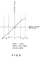
- Figure 9 is a graph showing the characteristics of an output signal from a pickup in relation to the wafer-to-mask deviation in the X and Y directions.
- Figure 10 is a flow chart, illustrating details of the processing to be made at step 604 in Figure 6.
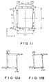
- Figure 11 is a schematic view, for explaining the calculation of elongation percentage of the wafer.
- Figures 12A and 12B are schematic views, respectively, for explaining the deviation due to wafer elongation and the deviation due to rotation, respectively.
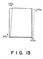
- Figure 13 is a schematic view, for explaining the state wherein one alignment mark of a wafer is out of a high-precision measurement zone.
- Figure 1 illustrates the structure of a part of a step-and-repeat type exposure apparatus (stepper) which pertains to the mask-to-wafer alignment and which is around an exposure stage.
- stepper step-and-repeat type exposure apparatus
- denoted at 1 is light for exposure (photoprinting) which is projected substantially along the Z-axis direction and which comprises X-rays contained in a synchrotron orbit radiation (SOR), for example.
- SOR synchrotron orbit radiation
- Denoted at 2 is a mask having formed thereon a pattern which is to be transferred onto a semiconductor wafer 3.
- Denoted at 4 is a mask 8 stage for rotationally moving the mask 2 along a plane (X-Y plane) parallel to the surface thereof; and at 5 is a ⁇ rough-motion stage for rotationally moving the wafer 3 along a plane (X-Y plane) parallel to the surface thereof.
- Denoted at 6 is a Z tilt stage which is effective to move the wafer 3 in the Z direction (movement toward the exposure light 1), in the wx direction (rotation about the X axis) and in the wy (rotation about the Y axis), respectively, when the wafer 3 is to be opposed to the mask 2 with a predetermined proximity gap in the Z-axis direction.
- Denoted at 7 is a 8 fine-motion stage for minutely rotating the wafer 3 in the X-Y plane; at 8 is an X fine-motion stage for minutely moving the wafer in the X direction; at 9 is a Y fine-motion stage for minutely moving the wafer in the Y direction; at 10 is an X rough-motion stage; and at 11 is a Y rough-motion stage.
- the ⁇ rough-motion stage 5, the Z tilt stage 6, the ⁇ fine-motion stage 7, the X fine-motion stage 8, the Y fine-motion stage 9, the X rough-motion stage 10 and the Y rough-motion stage 11, cooperate with each other to provide a wafer stage 24.
- each shot area on the wafer 3 is equipped with eight alignment marks, comprising regular marks and spare marks, formed on the scribe line around the shot area, wherein each regular mark and an associated spare mark are formed adjacent corresponding one of the four sides of that shot area.
- Each alignment mark is adapted to detect an error in the mask-to-wafer registration with respect to a direction which is parallel to the side at which that alignment mark is formed.
- a diffraction grating that provides an autoalignment (AA) mark 201 as well as an autofocusing (AF) mark 202, for detection of the spacing between the mask 2 and the wafer 3, has been formed on the wafer together with a semiconductor circuit pattern, in the preceding process.
- the mask 2 is provided with eight alignment marks (203, 204) associated with the alignment marks of the wafer 3, respectively, which mask alignment marks are formed of gold, for example, together with a semiconductor circuit pattern which is to be transferred to the wafer.
- 205 is a semiconductor laser (light emitting element); at 206 is a collimator lens for transforming the light emitted by the semiconductor laser 205 into a parallel light; at 207 is the light beam emitted by the semiconductor laser 205 and transformed by the collimator lens 206 into the parallel light; at 208 is an autoalignment (AA) light beam, to be received, which bears positional deviation information (AA information) given by an optical system constituted by the AA mark 201 of the wafer and the AA mark 203 of the mask; and at 209 is an autofocusing (AF) light beam, to be received, which bears gap information (AF information) given by an optical system constituted by the AF mark 202 of the wafer and the AF mark 204 of the mask.
- AA autoalignment
- AF autofocusing
- Denoted at 210 is an autoalignment (AA) sensor for converting the position of an autoalignment (AA) light spot 211, formed by the AA light beam 208, into an electric signal (AA information).
- the sensor 210 comprises a line sensor such as a CCD array.
- Denoted at 212 is an autofocusing (AF) sensor for converting the position of an autofocusing (AF) light spot 213, formed by the RE light beam 209, into an electric signal (AF information).
- the sensor 212 comprises a line sensor such as a CCD array.
- Figure 3 illustrates the structure of a control system of the exposure apparatus of Figure 1. While not shown in the drawings, the exposure apparatus of Figure 1 is equipped with a mirror unit for expanding the flux of X-rays, emitted from a SOR in the form of a horizontal sheet-like beam, in the vertical direction to provide an area beam; a main part unit which includes an alignment unit for aligning the mask and the wafer and an exposure unit for exposing the aligned mask and the wafer with the area X-ray beam; an attitude control unit for controlling the attitude of each of the mirror unit and the main-part unit; as well as a chamber and air conditioning unit for controlling the ambience around the mirror unit and the main-part unit.
- a mirror unit for expanding the flux of X-rays, emitted from a SOR in the form of a horizontal sheet-like beam, in the vertical direction to provide an area beam
- a main part unit which includes an alignment unit for aligning the mask and the wafer and an exposure unit for exposing the aligned mask and the wafer with the
- 301 is a main processor unit for controlling the operation of the apparatus as a whole; at 302 is a communication line for communicating the main processor unit 301 with the main-part unit; at 303 is a main-part side communication interface; at 304 is a main-part control unit; and at 305 is a pickup stage control means.
- Denoted at 306 and 308 are communication interfaces and denoted at 307 is a communication line, all of which are adapted to communicate, in the main-part unit, the main-part control unit 304 with fine AA/AF control means 309a, 309b, 309c and 309d for driving the fine alignment ⁇ , X and Y fine-motion stages and the mask ⁇ stage.
- Denoted at 310 and 312 are communication interfaces and denoted at 311 is a communication line all of which are adapted to communicate, in the main-part unit, the main-part control unit 304 with a stage control means 313 which controls the wafer prealignment and the stepwise movement.
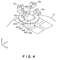
- Figure 4 illustrates the step-and-repeat exposure method.
- the mask ⁇ stage 4 which is driving means for the mask 2
- the wafer stage 24 which is driving means for the wafer 3
- the pickup stage 13 which is driving means for the pickup 12
- FIG 4 denoted at 12 (12a - 12d) are pickups for aligning the mask 2 and the wafer 3; at 418 is a pattern (to be transferred) formed on the mask; at 419 is a pattern, transferred, having been formed on the wafer in the preceding process; at 420 are alignment marks for mask alignment, to be used for aligning the mask 2 with a reference mark 14 ( Figure 1) provided on the wafer stage 24; at 421 are alignment marks formed on the mask, for aligning the mask pattern 418 with the transferred pattern 419; at 422 are alignment marks formed on the wafer for the same purpose; at 423 are projected light beams, projected from the pickups 12 for the same purpose; and at 401 are scribe lines defined between shot areas. The alignment marks 421 and 422 of the mask and the wafer are formed on these scribe lines.
- the mask 2 and the wafer 3 can be aligned with each other in the following manner: First, under the condition that the mask 2 and the wafer 3 are supported to be opposed to each other, the pickups 12a - 12d project light beams 423 and, through the corresponding alignment marks 421 and 422 of the mask and the wafer, the gap between the mask and the wafer is measured. On the basis of the information obtained from the four pickups, the amount of gap correcting drive is calculated and the wafer stage 24 is driven to set the gap between the mask and the wafer in respect to the z-axis direction, to be equal to the gap for exposure.
- the pickups 12a - 12d project light beams 423 again, and deviation between paired alignment marks 421 and 422 of the mask and the wafer, along a plane parallel to the surface of the mask or wafer, is measured.
- the amount of corrective drive of that shot area as a whole is calculated, and the mask ⁇ stage 4 and the wafer stage 24 are driven to bring the mask pattern 418 and the wafer pattern 419 into alignment with each other.
- the exposure operation is effected, whereby the mask pattern 418 is transferred onto the wafer 3.
- the wafer stage 24 is driven so that the next shot area comes to a position below the mask.
- the alignment and exposure operation is repeated, whereby exposures of all the shot areas are effected.
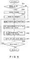
- Figure 5 is a flow chart, illustrating the flow of one patch of the step-and-repeat exposure sequence.
- the "one patch" is the unit with which the photoprinting of one wafer can be effected without replacement of a mask.
- the mask 2 and the wafer 3 are chucked to the mask ⁇ stage 4 and the wafer stage 24, respectively, while the pickup 12 projects light beam 423 to the alignment mark 421 of the mask for the AF (autofocusing) and AA (autoalignment) measurement.
- step 501 discrimination is made as to the necessity of mask replacement. If the exposure is to be effected by using the mask which is being chucked at this time, the sequence goes to step 504. If the mask is to be replaced by another, the sequence goes to step 502.
- step 502 the current mask is demounted from the mask stage 4, by using a mask traverser (not shown) and the demounted mask is stored into a mask cassette (not shown). Then, a mask to be used for the exposure is taken out of its mask cassette by using the mask traverser and it is chucked to the mask stage 4. Then, at step 503, the pickup 12 is used to align the mark 420, provided on the mask 2 for mask alignment, with the reference mark 14 provided on the wafer stage.
- the wafer stage 24 is driven to place the position on the wafer, just to be exposed (i.e. the current shot position, namely, the transferred pattern 419), to be opposed to the mask pattern 418.
- the alignment marks 421 and 422 of the mask and the wafer are used to measure the gap between the mask and the wafer, and the corrective drive for tilt and z-axis position is effected.
- the alignment marks 421 and 422 of the mask and the wafer are used to measure deviation between the mask and the wafer with respect to the X and Y directions, and corrective drive is effected to attain autoalignment. Details of such autoalignment (step 506) will be described later.
- step 507 the exposure of the current shot area is effected. Then, at step 508, discrimination is made as to whether there remains an unexposed shot area. If it remains, the sequence goes back to step 504. If it does not remain, the sequence is finished.
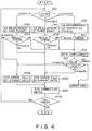
- Figure 6 is a flow chart, illustrating details of the autoalignment processing at step 506 in Figure 5. The illustrated pertains to autoalignment measurement and calculation of X, Y and ⁇ deviations as well as corrective drive, all related to one shot area.
- step 601 the layout of the shot area (current shot area), just to be exposed, on the wafer is checked.
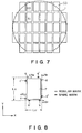
- Figure 7 shows exemplary shot layout of one wafer.
- Characters S1 - S3 denote shot areas.
- Figure 8 illustrates exemplary disposition of alignment marks of one shot area. Characters a - d denote regular marks for measurement of mask-to-wafer deviation, and characters a' - d' denote spare marks, all of which are provided on both the mask and the wafer. Each mark is adapted to detect deviation of its position, with respect to one of the X and Y directions.
- the marks a, a', b and b' are adapted for detection in the X direction, while the marks c, c', d and d' are adapted for detection in the Y direction. Accordingly, for detection of X, Y and ⁇ deviations of one shot area, it is necessary to measure at least those marks which are provided at three sides of the shot area.
- step 602 When the shot area S1 is going to be exposed, since this shot area as a whole is defined on the wafer, all the marks a - d can be measured. Therefore, the sequence goes to step 602 and, by the projection of autoalignment light beams 423 from the pickups 12, four-point measurement is effected. At step 603, the results of measurement are checked. At this step, the failure of measurement due to any fault or breakage of any mark, or a measurement error resulting from excessive deviation between the mask 2 and the wafer 3 is checked.
- Figure 9 illustrates the characteristics of the output signal from the pickup 12 in relation to the deviation between the wafer and the mask in the X and Y direction. While details will be described later with reference to step 604, the extent of zones I and II corresponds to the AA measurement range, and the extent of zone III corresponds to the region of measurement error which is excluded by step 603. If the measurement has been attained with respect to all the four marks, the four-point measurement is successful (OK) and sequence goes to step 604 whereat calculation of X, Y and ⁇ deviations is effected. Then, at step 605, corrective drive is effected to correct the X, Y and ⁇ errors. Then, at step 606, the amount of corrective drive is checked.
- step 604 If the quantity of correction, namely, the amount as obtained by calculation of deviation at step 604, is not greater than the tolerance, the AA processing is finished. If it is greater than the tolerance, sequence goes back to step 601. Details of the manner of calculating the X, Y and ⁇ deviations will be explained later by reference to Figure 10 and the like. If the measurement has been attained only with regard to three marks (step 603), three points are "OK" and the flow is combined into step 609 which is a part of the three-point measurement (steps 607 - 609) branched at step 601 from the sequence of the four-point measurement (steps 602 - 604) described above.
- step 612 is a part of the sequence of measurement using not greater than two points (steps 610 - 613), and a spare mark corresponding to the "NG" mark is measured.
- step 601 the flow goes from step 601 to step 607 whereat the AA measurement is effected to three points, excluding the mark a .
- step 608 the results of measurement are checked, like step 603. If the three points are "OK”, the flow goes to step 609. If "NG”, the flow goes to step 612.
- step 609 calculation of the quantities of X, Y and ⁇ corrections by using the three-point data is effected, including a case where the flow has been branched at step 603 from the four-point measurement sequence.
- Reference characters LX and LY each denotes the distance between those marks with which the deviation in the corresponding direction is to be detected, and a value obtained at step 1006, to be described later, or a design value is used therefor. Also, where measurement of any mark other than the mark a is not attainable, it is possible to detect three unknown quantities ⁇ X, ⁇ Y and ⁇ from the data obtained by measurement to three points other than the measurement-unattained mark. Then, at step 605, corrective drive is effected in the X, Y and ⁇ directions.
- the measurement is attainable only with regard to the marks b and c in Figure 8. While measurement of the mark d' is attainable, depending on the shape of each pickup and the disposition of the marks, there is a possibility of interference of the pickups. In consideration thereof, in the present embodiment, the measurement of the mark d' is effected later.
- step 601 the flow branches to step 610 and AA measurement is effected to two marks b and c. Then, at step 611, the results of measurement are checked and, at step 612, the insufficiency of the data is complemented. To this step 612, the flow having been branched from the four-point measurement or the three-point measurement is combined. Where the measurement has been attained only with regard to two points or less, like the shot area S3, since measurement is attainable with regard to the mark d', as described, the pickup 12d corresponding to the mark d is moved by the pickup stage 13d to the position above the spare mark d' and the mark d' measurement is effected.
- the flow has been branched from the four-point or three-point measurement in response to "NG"
- measurement of such a spare mark that corresponds to the "NG” mark is effected.
- the pickup 12 is moved, after completion of measurement it is necessary to move the pickup back to its preceding position for measurement of the next shot area.
- the total number of effective data is checked. If it is four points, the flow goes to step 604 and, if it is three points, the flow goes to step 609, and calculation of X, Y and ⁇ deviations is effected. If it is still not greater than two points, the flow goes to "error end” wherefrom a manual alignment operation is effected or, alternatively, the current shot area is skipped to the next shot area.
- the alignment may be effected in accordance with prediction based on the information related to an adjacent shot area or areas and, thereafter, the exposure may be effected.
- the flow may go to step 612, rather than step 609, so that measurement of a spare mark corresponding to the "NG" mark may be effected.
- the four-point measurement can reduce the effect of a measurement error as compared with the three-point measurement
- the throughput decreases with the four-point measurement because data measurement of additional one point, with the movement of the pickup, is executed to such a shot area the alignment itself of which is attainable by the three-point measurement. Thus, whether either one should be selected will be determined in consideration of time and precision.
- Figure 10 is a flow chart, illustrating details of the processing made at step 604 of Figure 6.
- the illustrated pertains to the sequence of calculation of X and Y and ⁇ deviations of one shot area, from the data obtained by four-point measurement.
- discrimination is made as to the necessity of calculation of elongation percentage of this shot area. If the elongation or contraction of the wafer due to a process is substantially uniform in the whole wafer, such elongation percentage calculation is necessary only with regard to a first shot area. With regard to a second shot area and those shot areas following it, corrective calculation can be made on the basis of the elongation percentage as determined by calculation with regard to the first shot area. Thus, the sequence skips to step 1007.
- the elongation percentage calculation is necessary, whether it is possible or not is discriminated at step 1002.
- the pickup 12 is moved to the position above a corresponding spare mark and, at step 1004, the mask-to-wafer deviation is measured by using the spare mark.
- the result of measurement is checked, like step 603 of Figure 6. If at least one spare mark in each of the X and Y directions has been measured, the measurement is "OK" and the sequence goes to step 1006. If not, the elongation percentage calculation is not possible and the sequence goes to step 1008.
- the elongation percentage of the wafer is calculated, from the measured values related to the regular marks, as measured at steps 602, 607 and 610 of Figure 6 as well as the measured values related to the spare marks, as measured at step 1004. Additionally, necessary correction of the mark intervals LX and LY is effected. Details of the manner of calculation will be explained by reference to Figure 11.
- the solid line depicts the design size of one shot area, while the broken line depicts the size of that shot area having been expanded.
- the solid line can be considered as representing the shape of the shot area on the mask, while the broken line can be considered as representing the shape of the shot area on the wafer.
- the measured data correction is effected on the basis of the elongation percentage as determined at step 1006.
- the already calculated elongation percentage is used. While the measured data represents the mask-to-wafer deviation at the mark position, the amount of deviation in the sense of alignment of the center of the shot area corresponds to one obtained by subtracting the amount of elongation from the detected deviation.
- step 1008 deviations ⁇ X, ⁇ Y, ⁇ X and ⁇ Y of the shot area are calculated.
- ⁇ X ( ⁇ XU+ ⁇ XD)/2
- ⁇ Y ( ⁇ YL+ ⁇ YR)/2
- ⁇ X ( ⁇ XU- ⁇ XD)/LX
- ⁇ Y ( ⁇ YL- ⁇ YR)/LY
- ⁇ X and ⁇ Y are the amounts of ⁇ rotational deviation as determined from the measured data in respect to the X and Y directions.
- the precision of measurement in the X direction is compared with that in the Y direction.
- the deviations ⁇ X and ⁇ Y as detected at step 1008 have the same value. Actually, however, usually they have different values, because of the measurement precision or distortion of the wafer or the like. In consideration thereof, one having better precision is adopted for the corrective drive.
- the detected deviation ⁇ Y is taken as the ⁇ rotational deviation ⁇ . If, on the other hand, both of the two measured values in the X direction are within the zone I, while at least one of the measured values in the Y direction is within the zone II, at step 1011 the detected deviation ⁇ X is taken as the rotational deviation ⁇ . If they are in the same zone, in both of the X and Y directions, the sequence goes to step 1012.
- step 1012 calculation is effected to determine the weighting coefficient n (0 ⁇ n ⁇ 1), for determining the ⁇ rotational deviation ⁇ by temporal coupling of ⁇ X and ⁇ Y, in an occasion where the measurement precision is the same in the X direction and in the Y direction.
- ⁇ X and ⁇ Y it is clear from the equation that, if the mark measurement precision is the same, one having a larger denominator has higher precision.
- LX and LY used in the calculation of the weighting coefficient n are those values having been corrected at step 1006 in consideration of the elongation percentage. If, however, the elongation percentage calculation is not attainable at step 1002 or 1005 and LX and LY are held at their design values, the weighting coefficient n can be calculated in the following manner: This method can be used in a case where the tendency of elongation/contraction of the wafer in each of the X and Y directions is predetected, from the direction of crystal growth of the wafer, for example.
- the deviations ⁇ X, ⁇ Y and ⁇ are determined after correcting the measured values on the basis of the elongation percentage.
- the branching based on discrimination at step 1009 may precede step 1008 to omit elongation correction to step 1010 or 1011.
- an alignment system usable with an original having a pattern and a substrate having a surface area on which the pattern of the original is to be printed said alignment system comprising:
- the discriminating means discriminates the number of pieces of correct mark detection information as outputted from said mark detecting means in accordance with layout information related to the layout of the surface region on the substrate.
- the discriminating means may discriminate the number of pieces of correct mark detection information as outputted from said mark detecting means in accordance with a mark detection error in said mark detecting means.
- the original and the substrate have surfaces opposed to each other and wherein said adjusting means corrects positional deviation between the original and the substrate along the opposed surfaces thereof.
- An alignment system is also described wherein the original and the substrate are opposed to each other with a spacing, and wherein said adjusting means controls the spacing between the original and the substrate.
- the calculating means may calculate the quantity of correction in accordance with a first formula in an occasion where the number of pieces of the mark detection information is not less than a first predetermined number, wherein said calculating means calculates the quantity of correction in accordance with a second formula in an occasion where the number of pieces of the mark detection information is less than the first predetermined number but not less than a second predetermined number, and wherein said calculating means calculates the quantity of correction in accordance with one of the first and second formulae after substitute mark detection information is complementarily supplied from said mark detecting means in an occasion where the number of pieces of the mark detection information is less than the second predetermined number.
- an alignment method usable with an original having a pattern and a substrate having a surface area on which the pattern of the original is to be printed said alignment method comprising the steps of:
Applications Claiming Priority (5)
| Application Number | Priority Date | Filing Date | Title |
|---|---|---|---|
| JP1248140A JP2785142B2 (ja) | 1989-09-26 | 1989-09-26 | アライメント装置 |
| JP248140/89 | 1989-09-26 | ||
| JP248139/89 | 1989-09-26 | ||
| JP1248139A JP2785141B2 (ja) | 1989-09-26 | 1989-09-26 | アライメント装置 |
| EP19900310481 EP0420574A3 (en) | 1989-09-26 | 1990-09-25 | Alignment system |
Related Parent Applications (1)
| Application Number | Title | Priority Date | Filing Date |
|---|---|---|---|
| EP19900310481 Division EP0420574A3 (en) | 1989-09-26 | 1990-09-25 | Alignment system |
Publications (2)
| Publication Number | Publication Date |
|---|---|
| EP0824225A2 true EP0824225A2 (de) | 1998-02-18 |
| EP0824225A3 EP0824225A3 (de) | 1998-03-04 |
Family
ID=26538621
Family Applications (2)
| Application Number | Title | Priority Date | Filing Date |
|---|---|---|---|
| EP19900310481 Withdrawn EP0420574A3 (en) | 1989-09-26 | 1990-09-25 | Alignment system |
| EP97203250A Withdrawn EP0824225A3 (de) | 1989-09-26 | 1990-09-25 | Ausrichtverfahren |
Family Applications Before (1)
| Application Number | Title | Priority Date | Filing Date |
|---|---|---|---|
| EP19900310481 Withdrawn EP0420574A3 (en) | 1989-09-26 | 1990-09-25 | Alignment system |
Country Status (2)
| Country | Link |
|---|---|
| US (1) | US6018395A (de) |
| EP (2) | EP0420574A3 (de) |
Families Citing this family (15)
| Publication number | Priority date | Publication date | Assignee | Title |
|---|---|---|---|---|
| US5426010A (en) * | 1993-02-26 | 1995-06-20 | Oxford Computer, Inc. | Ultra high resolution printing method |
| US5854671A (en) | 1993-05-28 | 1998-12-29 | Nikon Corporation | Scanning exposure method and apparatus therefor and a projection exposure apparatus and method which selectively chooses between static exposure and scanning exposure |
| US5995263A (en) * | 1993-11-12 | 1999-11-30 | Nikon Corporation | Projection exposure apparatus |
| US6130009A (en) * | 1994-01-03 | 2000-10-10 | Litel Instruments | Apparatus and process for nozzle production utilizing computer generated holograms |
| JP3047863B2 (ja) * | 1997-08-04 | 2000-06-05 | 日本電気株式会社 | アライメント方法 |
| TWI242112B (en) * | 1999-04-19 | 2005-10-21 | Asml Netherlands Bv | Lithographic projection apparatus and method of operating a lithographic projection apparatus |
| JP2000353657A (ja) * | 1999-06-14 | 2000-12-19 | Mitsubishi Electric Corp | 露光方法、露光装置およびその露光装置を用いて製造された半導体装置 |
| US6552790B1 (en) | 2001-02-20 | 2003-04-22 | Advanced Micro Devices, Inc. | System and method for facilitating wafer alignment by mitigating effects of reticle rotation on overlay |
| US6558883B2 (en) * | 2001-03-08 | 2003-05-06 | Infineon Technologies Ag | Apparatus and method for patterning a semiconductor wafer |
| JP2003133215A (ja) * | 2001-10-26 | 2003-05-09 | Oki Electric Ind Co Ltd | 露光装置及び露光方法 |
| US7054477B2 (en) * | 2002-11-13 | 2006-05-30 | Uni-Tek System, Inc. | Automatic accurate alignment method for a semiconductor wafer cutting apparatus |
| US20100045959A1 (en) * | 2008-08-21 | 2010-02-25 | Shin-Hsiang Chou | Photolithography apparatus with leveling element and method for leveling a wafer |
| US8432548B2 (en) * | 2008-11-04 | 2013-04-30 | Molecular Imprints, Inc. | Alignment for edge field nano-imprinting |
| JP2017067992A (ja) * | 2015-09-30 | 2017-04-06 | 株式会社オーク製作所 | 露光装置、露光装置のアライメント方法、およびプログラム |
| CN113506759B (zh) * | 2021-06-28 | 2024-02-02 | 上海华虹宏力半导体制造有限公司 | 关键尺寸在线监控结构的形成方法 |
Citations (3)
| Publication number | Priority date | Publication date | Assignee | Title |
|---|---|---|---|---|
| US4475122A (en) * | 1981-11-09 | 1984-10-02 | Tre Semiconductor Equipment Corporation | Automatic wafer alignment technique |
| US4780617A (en) * | 1984-08-09 | 1988-10-25 | Nippon Kogaku K.K. | Method for successive alignment of chip patterns on a substrate |
| US4833621A (en) * | 1986-06-11 | 1989-05-23 | Nikon Corporation | Method of and apparatus for aligning a substrate |
Family Cites Families (13)
| Publication number | Priority date | Publication date | Assignee | Title |
|---|---|---|---|---|
| JPS58108745A (ja) * | 1981-12-23 | 1983-06-28 | Canon Inc | 転写装置 |
| GB2146427B (en) * | 1983-08-01 | 1987-10-21 | Canon Kk | Semiconductor manufacture |
| US4564284A (en) * | 1983-09-12 | 1986-01-14 | Canon Kabushiki Kaisha | Semiconductor exposure apparatus |
| JPS6077422A (ja) * | 1983-10-04 | 1985-05-02 | Nec Corp | 電子ビ−ム露光による描画位置決め方法および電子ビ−ム露光装置の試料ホルダ− |
| US4830500A (en) * | 1985-04-15 | 1989-05-16 | Canon Kabushiki Kaisha | Alignment device |
| US4676630A (en) * | 1985-04-25 | 1987-06-30 | Canon Kabushiki Kaisha | Exposure apparatus |
| US4748477A (en) * | 1985-04-30 | 1988-05-31 | Canon Kabushiki Kaisha | Exposure apparatus |
| US4749867A (en) * | 1985-04-30 | 1988-06-07 | Canon Kabushiki Kaisha | Exposure apparatus |
| US4704033A (en) * | 1986-03-06 | 1987-11-03 | Micronix Corporation | Multiple wavelength linear zone plate alignment apparatus and method |
| US4918320A (en) * | 1987-03-20 | 1990-04-17 | Canon Kabushiki Kaisha | Alignment method usable in a step-and-repeat type exposure apparatus for either global or dye-by-dye alignment |
| JP2623090B2 (ja) * | 1987-06-03 | 1997-06-25 | キヤノン株式会社 | 距離測定装置 |
| US4958160A (en) * | 1987-08-31 | 1990-09-18 | Canon Kabushiki Kaisha | Projection exposure apparatus and method of correcting projection error |
| EP0412756B1 (de) * | 1989-08-07 | 1995-10-25 | Canon Kabushiki Kaisha | Belichtungsvorrichtung |
-
1990
- 1990-09-25 EP EP19900310481 patent/EP0420574A3/en not_active Withdrawn
- 1990-09-25 EP EP97203250A patent/EP0824225A3/de not_active Withdrawn
-
1996
- 1996-12-16 US US08/766,928 patent/US6018395A/en not_active Expired - Fee Related
Patent Citations (3)
| Publication number | Priority date | Publication date | Assignee | Title |
|---|---|---|---|---|
| US4475122A (en) * | 1981-11-09 | 1984-10-02 | Tre Semiconductor Equipment Corporation | Automatic wafer alignment technique |
| US4780617A (en) * | 1984-08-09 | 1988-10-25 | Nippon Kogaku K.K. | Method for successive alignment of chip patterns on a substrate |
| US4833621A (en) * | 1986-06-11 | 1989-05-23 | Nikon Corporation | Method of and apparatus for aligning a substrate |
Also Published As
| Publication number | Publication date |
|---|---|
| EP0824225A3 (de) | 1998-03-04 |
| EP0420574A2 (de) | 1991-04-03 |
| US6018395A (en) | 2000-01-25 |
| EP0420574A3 (en) | 1992-04-22 |
Similar Documents
| Publication | Publication Date | Title |
|---|---|---|
| EP0420700B1 (de) | Belichtungsvorrichtung | |
| US7202938B2 (en) | Off-axis levelling in lithographic projection apparatus | |
| US6481003B1 (en) | Alignment method and method for producing device using the alignment method | |
| US6649923B2 (en) | Positional deviation detecting method and device manufacturing method using the same | |
| EP1195647B1 (de) | Verfahren zur Detektion einer Oberflächenlage und Abtastbelichtungsverfahren unter Verwendung derselbe | |
| US6018395A (en) | Alignment system | |
| US5323016A (en) | Focusing method | |
| US6416912B1 (en) | Method of manufacturing microdevice utilizing combined alignment mark | |
| US6501532B2 (en) | Exposure apparatus and method of controlling the same | |
| US6124922A (en) | Exposure device and method for producing a mask for use in the device | |
| EP0702272B1 (de) | Belichtungsapparat und Belichtungsverfahren | |
| JP2000012455A (ja) | 荷電粒子線転写露光装置及び荷電粒子線転写露光装置におけるマスクと感応基板の位置合わせ方法 | |
| US4881100A (en) | Alignment method | |
| US6750950B1 (en) | Scanning exposure method, scanning exposure apparatus and making method for producing the same, and device and method for manufacturing the same | |
| JP2868548B2 (ja) | アライメント装置 | |
| JP2785141B2 (ja) | アライメント装置 | |
| JPH0737785A (ja) | 露光装置およびそのアライメント方法 | |
| JPH1116827A (ja) | 面情報検出装置及びそれを用いた投影露光装置 | |
| JP2785142B2 (ja) | アライメント装置 | |
| JP2646417B2 (ja) | 露光装置 | |
| JP3420401B2 (ja) | 位置検出装置および方法、半導体露光装置ならびに半導体デバイスの製造方法 | |
| JP2000208391A (ja) | 露光装置および方法ならびにデバイス製造方法 | |
| JPH11219897A (ja) | 検出方法、走査露光方法、走査型露光装置、及びデバイス製造方法 | |
| JPH05326364A (ja) | 位置決め装置 | |
| JPH03185810A (ja) | 露光装置 |
Legal Events
| Date | Code | Title | Description |
|---|---|---|---|
| PUAI | Public reference made under article 153(3) epc to a published international application that has entered the european phase |
Free format text: ORIGINAL CODE: 0009012 |
|
| PUAL | Search report despatched |
Free format text: ORIGINAL CODE: 0009013 |
|
| AC | Divisional application: reference to earlier application |
Ref document number: 420574 Country of ref document: EP |
|
| AK | Designated contracting states |
Kind code of ref document: A2 Designated state(s): DE FR GB IT NL |
|
| AK | Designated contracting states |
Kind code of ref document: A3 Designated state(s): DE FR GB IT NL |
|
| 17P | Request for examination filed |
Effective date: 19980716 |
|
| 17Q | First examination report despatched |
Effective date: 20011025 |
|
| STAA | Information on the status of an ep patent application or granted ep patent |
Free format text: STATUS: THE APPLICATION HAS BEEN WITHDRAWN |
|
| 18W | Application withdrawn |
Effective date: 20160720 |