EP0814514A2 - A semiconductor memory device including a capacitor - Google Patents
A semiconductor memory device including a capacitor Download PDFInfo
- Publication number
- EP0814514A2 EP0814514A2 EP97304161A EP97304161A EP0814514A2 EP 0814514 A2 EP0814514 A2 EP 0814514A2 EP 97304161 A EP97304161 A EP 97304161A EP 97304161 A EP97304161 A EP 97304161A EP 0814514 A2 EP0814514 A2 EP 0814514A2
- Authority
- EP
- European Patent Office
- Prior art keywords
- layer
- oxide
- group
- upper electrode
- semiconductor memory
- Prior art date
- Legal status (The legal status is an assumption and is not a legal conclusion. Google has not performed a legal analysis and makes no representation as to the accuracy of the status listed.)
- Granted
Links
Images
Classifications
-
- H—ELECTRICITY
- H10—SEMICONDUCTOR DEVICES; ELECTRIC SOLID-STATE DEVICES NOT OTHERWISE PROVIDED FOR
- H10B—ELECTRONIC MEMORY DEVICES
- H10B12/00—Dynamic random access memory [DRAM] devices
-
- H—ELECTRICITY
- H01—ELECTRIC ELEMENTS
- H01L—SEMICONDUCTOR DEVICES NOT COVERED BY CLASS H10
- H01L28/00—Passive two-terminal components without a potential-jump or surface barrier for integrated circuits; Details thereof; Multistep manufacturing processes therefor
- H01L28/40—Capacitors
-
- H—ELECTRICITY
- H10—SEMICONDUCTOR DEVICES; ELECTRIC SOLID-STATE DEVICES NOT OTHERWISE PROVIDED FOR
- H10B—ELECTRONIC MEMORY DEVICES
- H10B12/00—Dynamic random access memory [DRAM] devices
- H10B12/01—Manufacture or treatment
Definitions
- the present invention relates to a memory device and a manufacturing method thereof, and more particularly, to a capacitor of a semiconductor memory device comprised of a ferroelectric material as a dielectric film, and a manufacturing method thereof.
- DRAMs dynamic random access memories
- the unit cell area decreases.
- cell capacitance is reduced due to the reduction in the area of the memory cell, readout of the memory cell is deteriorated and the soft error ratio increases.
- excessive amounts of power is required for device operation at low voltage. Accordingly, it is necessary to ensure a large enough cell capacitance so as not to deteriorate the operation characteristics of the memory cell.
- a first method is to form a thinner dielectric film
- a second method is to increase the effective area of the capacitor
- a third method is to use material having a high dielectric constant as the dielectric film.
- ferroelectric material for example, an oxide of a Perovskite structure having a high dielectric constant, such as PbZrTiO 3 (PZT) or BaSrTiO 3 (BST), has recently been proposed.
- the ferroelectric material has a spontaneous polarization phenomenon, unlike a conventional dielectric film such as a silicon oxide film, a silicon nitride film or a tantalum oxide (Ta 2 O 5 ) film, and a high dielectric constant of hundreds to approximately 1,000 under a bulk state. Even though the dielectric film of the ferroelectric material is formed to 500 ⁇ or thicker, the equivalent oxide thickness can be formed as thin as 10 ⁇ or less.
- the electrode material formed on and under the dielectric film is important.
- the following conditions must be met for an electrode material of a capacitor using a ferroelectric material.
- a film of a Perovskite structure should be formed on the electrode.
- a low dielectric film should not be formed on a interface between the electrode and a film having the ferroelectric material.
- silicon or components of the ferroelectric material should not be mutually diffused.
- the electrode should be easy to pattern.
- Platinum group metals having oxidation-resistance and high conductivity can be used such as Platinum (Pt), Ruthenium (Ru) or Iridium (Ir), and a conductive oxide such as IrO 2 or RuO 2 for electrodes of the capacitor in which the ferroelectric material is used as the dielectric film.
- a resistor of a periphery region is formed of material for forming an upper electrode of the capacitor.
- the capacitor having a ferroelectric material in which electrodes formed of the platinum group metals or an oxide thereof are used as the upper electrode the resistance of the electrodes is excessively low.
- the upper electrode of the capacitor cannot be used as the resistor of the periphery region.
- the resistor used for the memory device is used for a voltage generator and a RC delay in the periphery region, and requires a resistance of several of k ⁇ .
- the resistor of the periphery region is formed of polysilicon for gate electrodes of a cell region, and in the case that the desired resistance is high, it is formed of polysilicon for an upper electrode of the capacitor.
- the sheet resistance of gate electrodes having a structure of a low resistance or the upper electrode is excessively low. Accordingly, in the case that the materials are used for a resistor of the periphery region, a length of the resistor which becomes longer in inverse proportion to the sheet resistance, makes it difficult to integrate. For example, in the case that 1 ⁇ m of resistor width is used, in order to form a resistor of 1k ⁇ , polysilicon having a sheet resistance of 100 ⁇ / ⁇ requires a length of 10 ⁇ m, however, WSi x /polysilicon having a sheet resistance of 2 ⁇ / ⁇ requires a length of 500 ⁇ m. Thus, the resistor occupies much of the periphery region. Also, in the case that platinum (Pt) is used for the upper electrode of the ferroelectric material, the upper electrode of the capacitor cannot be used for the resistor of the periphery region.
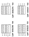
- FIG. 1 is a sectional view for illustrating a first conventional method for forming a capacitor having a ferroelectric material, which is described in "VLSI Technology Digest of Technical, pp. 149-150, in 1994 by Mitsubishi Co".
- the capacitor has a structure of Pt 2/BST 4/Pt 6.
- platinum Pt has a low sheet resistance
- the upper electrode 6 cannot be used for the resistor of the periphery region.
- adhesion of the platinum 6 of the upper electrode to an aluminum film 8 of an interconnection layer formed on the platinum layer 6 is poor.
- FIG. 2 is a sectional view for illustrating a second conventional manufacturing method of a capacitor having a ferroelectric material, described in U.S. Patent No. 5,005,012.
- FIG. 2 a method of forming a multilayered upper electrode is shown.
- a conductive barrier layer 17 is inserted between an upper electrode 16 and an interconnection metal layer 18.
- the structure shown in FIG. 2 has advantage that the adhesive characteristic of the upper electrode 16 to the interconnection metal layer 18 is enhanced, whereas the structure has disadvantage that the upper electrode of the capacitor cannot be used as a resistor of the periphery region.
- Reference numeral 12 denotes a lower electrode
- reference numeral 13 denotes an adhesion/barrier layer for enhancing adhesion and preventing mutual reaction between the lower electrode 12 to a dielectric film 14.
- FIG. 3A is a sectional view for illustrating a third conventional manufacturing method of a capacitor having a ferroelectric material described in Japanese Patent No. JP06-125057.
- a metal layer 37a having a high melting point such as titanium nitride (TiN) and tungsten-titanium (TiW) is inserted, to thereby prevent mutual diffusion of Al and Pt.
- Reference numeral 32 denotes a lower electrode and reference numeral 34 denotes a dielectric film.
- FIG. 3B is a sectional view for illustrating a fourth conventional manufacturing method of a capacitor having a ferroelectric material described in U.S. Patent No. 4,982,309. Between conductive oxide electrode 36 and a metal interconnection layer 38, a barrier layer 37b formed of a metal such as Ruthenium or Iridium, is inserted. Reference numeral 32 denotes a lower electrode and reference numeral 34 denotes a dielectric film.
- the upper electrode of the capacitor cannot be used for a resistor of a periphery region like in FIGs. 1 and 2.
- the upper electrode formed of platinum 36 and a metal layer 37a having a high melting point, contacts an interlayer insulating film (not shown), which is based on a silicon oxide such as Borophosphorus Silicate Glass (BPSG) or Undoped Silicate Glass (USG).
- BPSG Borophosphorus Silicate Glass
- USG Undoped Silicate Glass
- an object of the present invention to provide a semiconductor memory device in which an upper electrode can be used as a resistance layer of a periphery region and in which adhesion of the upper electrode to an interconnection layer is enhanced, and further, to prevent deterioration of characteristics of the capacitor by reducing stress between the upper electrode and the interlayer insulating film.
- a semiconductor memory device comprising a lower electrode, a dielectric film, an upper electrode and a first material layer.
- the lower electrode and upper electrode are formed of one selected from the group consisting of a platinum group metal such as Pt, Ru, Ir, Pd and Os, and insulating conductive oxide such as IrO 2 , platinum oxide, Osmium oxide, Indium oxide, Indium Tin Oxide (ITO) and RuO 2 .
- the dielectric film is formed of an oxide having Perovskite structure such as PZT, PbTiO 3 , PbLaTiO 3 , BaTiO 3 , Bi 4 Ti 3 O 12 , SrBi 2 Ta 2 O 9 , BST (BaSrTiO 3 ) and STO (SrTiO 3 ).
- the first material layer formed on the upper electrode has sheet resistance of 5 ⁇ 500 ⁇ / ⁇ .
- the first material layer further comprises a first barrier layer and an interconnection layer on the first barrier layer, wherein the first barrier layer prevents reaction of the first material layer and the interconnection layer.
- a second barrier layer can be formed to prevent reaction of the upper electrode and first material layer between the upper electrode and first material layer.
- a manufacturing method of a semiconductor memory device By the method, a lower electrode is formed on a semiconductor substrate. A dielectric film is formed on the lower electrode. A conductive layer for an upper electrode is formed on the dielectric film, and then the conductive layer for the upper electrode and the dielectric film are patterned. A first material layer capable of being used as a resistor of a periphery region is formed on the resultant structure. An interlayer insulating film is formed on the resultant structure first material layer and then patterned, to form a contact hole for connecting an interconnection layer to the upper electrode. The interconnection layer is formed on the resultant structure where the contact hole is formed.
- the upper and lower electrodes are formed of one selected from the group consisting of a platinum group metal such as and a conductive oxide such as Pt, Ru, Ir, Pd and Os, and insulating conductive oxide such as IrO 2 , platinum oxide, Osmium oxide, Indium oxide, Indium Tin Oxide (ITO) and RuO 2 .
- a platinum group metal such as and a conductive oxide such as Pt, Ru, Ir, Pd and Os
- insulating conductive oxide such as IrO 2 , platinum oxide, Osmium oxide, Indium oxide, Indium Tin Oxide (ITO) and RuO 2 .
- the dielectric film is formed of an oxide having Perovskite structure such as PZT, PbTiO 3 , PbLaTiO 3 , BaTiO 3 , Bi 4 Ti 3 O 12 , SrBi 2 Ta 2 O 9 , BST (BaSrTiO 3 ) and STO (SrTiO 3 ).
- the first material layer having sheet resistance of 5 ⁇ 500 ⁇ / ⁇ is one selected from the group consisting of polysilicon, tungsten silicide, SiN and Al 2 O 3 .
- a semiconductor layer or an insulator layer is deposited on the upper electrode of the capacitor, so that the semiconductor layer or the insulator layer can be used as the resistor of the periphery region without deterioration of capacitor characteristics, and adhesion of the upper electrode to the interconnection layer and the upper electrode of Pt to the dielectric film can also be enhanced.
- reference numeral 40 denotes a semiconductor substrate
- reference numeral 42 denotes a field oxide film for defining an active region and a non-active region
- reference numeral 44 denotes a gate insulating film of an oxide film, a nitride film or an ONO film
- reference numeral 46 denotes a gate of polysilicon or polycide
- reference numeral 48 denotes a bit line connected to a drain of a transistor (not shown)
- reference numerals 50 and 64 denote interlayer insulating films
- reference numeral 52 denotes a plug for connecting a lower electrode of a capacitor to a source of the transistor (not shown)
- reference numeral 54 denotes a lower electrode of the capacitor
- reference numeral 56 denotes a dielectric film
- reference numeral 58 denotes an upper electrode of the capacitor
- reference numeral 62a denotes a first material layer formed of a semiconductor or an insulator
- reference numeral 62b denotes a resist
- a capacitor having ferroelectric material including the lower electrode 54, the dielectric film 56 and the upper electrode 58, the upper and lower electrodes 58 and 54 are formed of a material selected from the group consisting of Pt, Ru, Ir, Pd, IrO 2 , a platinum oxide, an osmium oxide, an indium oxide, an Indium Tin Oxide (ITO) and RuO 2 .
- the dielectric film 56 is formed of one selected from the group consisting of an oxide having a Perovskite structure such as PZT, PbTiO 3 , PbLaTiO 3 , BaTiO 3 , BaSrTiO 3 and SrTiO 3 or Bi 4 Ti 3 O 12 and SrBi 2 Ta 2 O 9 .
- an oxide having a Perovskite structure such as PZT, PbTiO 3 , PbLaTiO 3 , BaTiO 3 , BaSrTiO 3 and SrTiO 3 or Bi 4 Ti 3 O 12 and SrBi 2 Ta 2 O 9 .
- first material layers 62a and 62b which can enhance adhesion of an interconnection layer to the upper electrode and can be used as a resistor of the periphery region and are formed of a semiconductor or an insulator having sheet resistance of approximately 5 ⁇ 500 ⁇ / ⁇ , are formed.
- the first material layers 62a and 62b are formed of one selected from the group consisting of a semiconductor such as polysilicon or WSix, and an insulator such as SiN, Al 2 O 3 , TiSi 2 N y , TaSi x N y and Ti x Al y N z .
- first material layers 62a and 62b are formed of a semiconductor such as polysilicon or silicide
- a contact hole for connecting the interconnection layer 70 of a cell region to the first material layer thereof may be formed directly on a surface of the first material layer 62a.
- a first barrier layer 68 can be further included.
- the first barrier layer 68 is formed of one selected from the group consisting of a double film of Ti/TiN, TiSi x N y , TaSi x N y , Ir and IrO 2 .
- a second barrier layer 76 for preventing mutual reaction of the upper electrode and the first material layer may be further included.
- the second barrier layer 76 can be formed of the same material as that of the first barrier layer 68.
- first material layers 78a and 78b formed between an upper electrode 58 and an interconnection layer 70 can be formed of an insulator instead of a semiconductor such as polysilicon.
- the first material layer formed of a semiconductor or an insulator having sheet resistance which can be used for a resistor of a periphery region, is further included between the upper electrode of the capacitor having ferroelectric material and the interconnection layer.
- the adhesion of the interconnection layer to the upper electrode of the capacitor can be enhanced, and the first material layer can form the resistor of the periphery region.
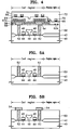
- FIG. 5A shows the step of forming a transistor and a contact hole.
- the step is performed by forming an isolation film for isolating a semiconductor substrate into an active region and a non-active region, forming a transistor at the active region of the semiconductor substrate, forming a bitline connected to a drain of the transistor, forming an interlayer insulating film on the resultant structure where the bitline is formed, and forming a plug for connecting a source of the transistor and a lower electrode of the capacitor.
- a field oxide film 42 is formed on a semiconductor substrate 40 using a typical isolation process such as local oxidation of silicon (LOCOS), and then a transistor having a gate insulating film 44, a gate electrode 46 and a source/drain (not shown) are formed in a usual manner.
- LOCOS local oxidation of silicon
- a bitline 48 contacting the drain of the transistor is formed, and then an insulating film is deposited on the entire surface of the resultant structure where the bitline 48 is formed, to thereby form an interlayer insulating film 50.
- the interlayer insulating film 50 is partially etched, to thereby form a contact hole.
- the contact hole is filled with conductive material, to thereby form a plug 52 for connecting a source of the transistor to the lower electrode of the capacitor.
- FIG. 5B shows the step of forming lower electrode 54 of the capacitor.
- the step is performed by depositing a platinum group metal or a conductive oxide, thereby forming a conductive layer, and patterning the conductive layer.
- conductive material for forming the lower electrode of the capacitor on the resultant structure, where the plug 52 is formed is deposited to a thickness of approximately 100 ⁇ 3,000 ⁇ , to thereby form a conductive layer. Then, the conductive layer is patterned using a conventional photolithography method, to thereby form the lower electrode 54 of the capacitor.
- the material for forming the lower electrode 54 of the capacitor is, one selected from the group consisting of a conductive material having high conductivity and oxidation-resistance such as Pt, Ru, Ir, Pd or Os, a conductive oxide such as IrO 2 , platinum oxide (PtO), Osmium oxide (OsO 2 ) Indium oxide (In 2 O 3 ), Indium Tin Oxide (ITO), RuO 2 , and a combination of the conductive material with the conductive oxide.
- a conductive material having high conductivity and oxidation-resistance such as Pt, Ru, Ir, Pd or Os
- a conductive oxide such as IrO 2 , platinum oxide (PtO), Osmium oxide (OsO 2 ) Indium oxide (In 2 O 3 ), Indium Tin Oxide (ITO), RuO 2
- a combination of the conductive material with the conductive oxide is, one selected from the group consisting of a conductive material having high conductivity and
- a sputtering or chemical vapor deposition (CVD) is used to deposit the electrode material.
- the metal is used as a target under an argon (Ar) atmosphere, at a substrate temperature of 20 ⁇ 500°C and at a chamber pressure of 1 ⁇ 10mTorr.
- Ar argon
- the metal is used as a target under an atmosphere of mixed gases of Ar with O 2 of 5 ⁇ 50% and further, at a chamber pressure of 1 ⁇ 10mTorr.
- platinum-hexafluoroacetyl acetonate (Pt-HFA) 2 is used as a platinum source.
- Pt-HFA platinum-hexafluoroacetyl acetonate
- Ar of 100 ⁇ 1,000sccm is provided at a chamber pressure of 10mTorr ⁇ 10Torr and at substrate temperature of 100 ⁇ 500°C.
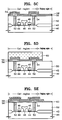
- FIG. 5C shows the step of forming a dielectric film 56 and a conductive layer 58 for an upper electrode of a capacitor.
- the step is performed by depositing ferroelectric material on the resultant structure of FIG. 5B, thereby forming a dielectric film, and depositing a platinum group metal or a platinum oxide, thereby forming a conductive layer.
- ferroelectric material such as PZT
- a lower electrode of the capacitor is formed, by sputtering or CVD, thereby forming the dielectric film 56.
- a platinum group metal or a conductive oxide is deposited on the dielectric film in the same manner as that for forming the lower electrode 54, to thereby form the conductive layer 58 for an upper electrode.
- the material for forming the dielectric film 56 one selected from the group consisting of an oxide having a Perovskite structure such as PZT, PbTiO 3 , PbLaTiO 3 , BaTiO 3 , BST (BaSrTiO 3 ) and STO (SrTiO 3 ) or Bi 4 Ti 3 O 12 , SrBi 2 Ta 2 O 9 can be used.
- BST is used as a target under Ar and O 2 atmosphere.
- a substrate temperature of 450 ⁇ 650°C and a chamber pressure of 1 ⁇ 10mTorr are maintained.
- Ba(DPM) 2 , Sr(DPM) 2 or Ti(DPM) 2 is used as a main component of the CVD source and an oxide gas including O 2 _and N 2 O of 10 ⁇ 50% with Ar is provided into the chamber, in which the substrate temperature is 450 ⁇ 800°C and the chamber pressure is 0.1 ⁇ 10Torr.
- FIG. 5D shows the step of photolithography for patterning the conductive layer 58 for an upper electrode.
- the step is performed by forming a photo resist pattern on the conductive layer for the upper electrode and patterning the conductive layer for the upper electrode and the dielectric film.
- the conductive layer 58 for the upper electrode of the periphery region and the dielectric film 56 thereof are etched, using the photo resist pattern 60 as a mask.
- the conductive layer 58 for the upper electrode can be etched by wet or dry etching.
- a mixture of HCl and HNO 3 can be used for wet-etching, or a mixed gas of O 2 and Cl 2 can be used for the dry-etching.
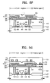
- FIG. 5E shows the step of forming a first material layer 62.
- the step is performed by removing the photo resist pattern and depositing polysilicon on the resultant structure where the photo resist pattern is removed.
- the photo resist pattern is eliminated, and then on the entire surface of the resultant structure of the cell region and the periphery region, a semiconductor or insulator such as polysilicon, which can be used as a resistor of the periphery region, is deposited, to thereby form the first material layer 62.
- the first material layer 62 can be used as a barrier layer for enhancing adhesion of the upper electrode to the interconnection layer in the cell region and can be used for a resistor in the periphery region.
- SiH 4 or SiH 2 Cl 2 is used as a source and a dopant source including PH 3 is implanted into a chamber, and a CVD method is used at a substrate temperature of 550 ⁇ 750°C.
- the thickness and doping concentration of the polysilicon film 62 should be controlled appropriately such that the sheet resistance of the polysilicon film is 5 ⁇ 500 ⁇ / ⁇ , which is the sheet resistance Rs required for resistance of the periphery region. It is preferred that the thickness of the polysilicon film is approximately 100 ⁇ 3,000 ⁇ .
- the doping concentration of the polysilicon film is controlled by adding a dopant into the chamber during a CVD process or depositing undoped polysilicon, and then performing ion-implantation or diffusion.
- silicide such as WSi x TiSi x , TiSi x N y and TaSi x N y or an insulating film such as SiN or Al 2 O 3 , instead of the polysilicon film 62, can be used.
- FIG. 5F shows the step of forming an interlayer insulating film 64 and a contact hole 66.
- the step is performed by patterning a polysilicon film, depositing an insulator on the patterned polysilicon, thereby forming the interlayer insulating film, and etching the interlayer insulating film, thereby forming a contact hole for connecting the upper electrode of the capacitor and the interconnection layer thereof.
- the first material layer is patterned by a conventional photolithography, to thereby form a first material layer pattern, which can be used for the barrier layer 62a for enhancing adhesion of the upper electrode 58 of the capacitor to the interconnection layer thereof, and can be used for the resistor 62b having a predetermined resistance in the periphery region.
- one selected from the group consisting of BPSG, PSG, SG, SOG, USG, and a combination thereof is deposited on the resultant structure to a predetermined thickness of approximately 2,000 ⁇ 10,000 ⁇ , to thereby form an interlayer insulating film 64.
- the interlayer insulating film 64 is partially etched by photolithography, to thereby form a contact hole 66 for connecting the upper electrode of the capacitor to the interconnection layer thereof.
- the contact hole 66 can be formed, with a surface of the first material layer 62a exposed or with a surface of the upper electrode layer 58 portion under the first material layer exposed.
- FIG. 5G shows the step of forming a barrier layer 68, an interconnection layer 70 and a protective film 72.
- the step is performed by forming the barrier layer 68 on the resultant structure where the contact hole is formed, and depositing interconnection metal on the resultant structure, thereby forming the interconnection layer 70, patterning the interconnection layer and the barrier layer, and forming the protective film 72 on the resultant structure.
- a material selected from the group consisting of a double film of Ti/TiN, TiSi x N y , TaSi x 4 y , Ir and IrO 2 is deposited to a thickness of 100 ⁇ 1,000 ⁇ , to thereby form the barrier layer 68 for preventing mutual diffusion of the first material layer 62a and the interconnection layer and forming an ohmic contact between the first material layer 62a and the interconnection layer.
- a metal such as Aluminum for interconnection, is deposited to a thickness of approximately 3,000 ⁇ 10,000 ⁇ , and then the barrier layer 68 and the interconnection layer 70 are patterned by photolithography. Then, a process of forming the protective layer 72 and a succeeding process are performed by a typical manufacturing process of a DRAM.
- a resistor of the periphery region is deposited on the upper electrode layer of the capacitor having ferroelectric material.
- the resistor of the periphery region can be concurrently formed during formation of the capacitor, and adhesion of the upper electrode layer to the interconnection layer is enhanced, and further reliability can be enhanced.
- the first material layer prevents stress due to reaction with an interlayer insulating film to be deposited.
- the second embodiment is suitable for preventing the mutual diffusion of an upper electrode of a capacitor and a first material layer, i.e., for forming the upper electrode by Pt.
- the manufacturing method of this embodiment involves the processes of forming a first barrier layer which is formed of Platinum on an upper electrode layer 74, forming the first material layer on the first barrier layer, exposing the first material layer of the periphery region by photolithography and patterning the first material layer, the first barrier layer and the upper electrode layer.
- a Platinum layer 74 is formed as a conductive layer for the upper electrode. Then, in order to prevent reaction of the Pt layer 74 and a polysilicon film 62a formed at the first material layer, material for preventing reaction of Pt and polysilicon, i.e., TiN, Ir, IrO 2 , RuO 2 or Ru, TiSi x N y , TaSi x N y is deposited on the platinum layer 74 to a thickness of 100 ⁇ 1,000 ⁇ by sputtering, to thereby form a first barrier layer 76.
- the processes of forming the polysilicon film, patterning the upper electrode layer, or forming a contact hole, which are performed by the same method as that in the first embodiment, will not be described.
- a barrier layer for preventing the mutual reaction of the first material layer and the upper electrode layer is also formed, to thereby enhance reliability.
- the third embodiment is suitable for cases where an insulator instead of a semiconductor such as polysilicon is used as the first material layers 78a and 78b formed between the upper electrode 58 and the interconnection layer 70.
- the insulator is SiO 2 , Al 2 O 3 or SiN.
- Other processes performed by the same method as that in the first embodiment will not be described.
- a contact hole for connecting the interconnection layers 68 and 70 to the upper electrode 58 in a cell region is formed by etching the insulator layer 78a to expose a surface of the upper electrode 58.
- a semiconductor layer or an insulator layer is deposited on the upper electrode of the capacitor. Accordingly, the semiconductor layer or the insulation layer can be used for a resistor of a periphery region without deterioration of capacitor characteristics, adhesion of the upper electrode to the interconnection layer can be enhanced, and adhesion of the upper electrode to a dielectric film is improved. Also, a layer without stress, which is caused by a reaction with the interlayer insulating film, is formed between the electrode and the interlayer insulating film, to thereby prevent deterioration of capacitance in a subsequent process.
Abstract
Description
- The present invention relates to a memory device and a manufacturing method thereof, and more particularly, to a capacitor of a semiconductor memory device comprised of a ferroelectric material as a dielectric film, and a manufacturing method thereof.
- In general, in semiconductor memory devices, such as dynamic random access memories (DRAMs), as integration increases, the unit cell area decreases. When cell capacitance is reduced due to the reduction in the area of the memory cell, readout of the memory cell is deteriorated and the soft error ratio increases. Also, excessive amounts of power is required for device operation at low voltage. Accordingly, it is necessary to ensure a large enough cell capacitance so as not to deteriorate the operation characteristics of the memory cell.
- Various methods for increasing capacitance of the memory cell within a defined cell area have been proposed, of which most fall into one of three methods. That is, a first method is to form a thinner dielectric film, a second method is to increase the effective area of the capacitor, and a third method is to use material having a high dielectric constant as the dielectric film. By the first method of forming a dielectric film having a thickness of 100Å or less, reliability of the device is deteriorated by the generation of a Fowler-Nordheim current. Thus, it is difficult to apply the method to a memory device having a large capacity. By the second method of forming a three-dimensional structure of the capacitor, a complicated process is required. Thus, a rise in the production cost is inevitable.
- Accordingly, the third method, by which a dielectric film is formed using a dielectric material (hereinafter referred to ferroelectric material), for example, an oxide of a Perovskite structure having a high dielectric constant, such as PbZrTiO3 (PZT) or BaSrTiO3 (BST), has recently been proposed. The ferroelectric material has a spontaneous polarization phenomenon, unlike a conventional dielectric film such as a silicon oxide film, a silicon nitride film or a tantalum oxide (Ta2O5) film, and a high dielectric constant of hundreds to approximately 1,000 under a bulk state. Even though the dielectric film of the ferroelectric material is formed to 500Å or thicker, the equivalent oxide thickness can be formed as thin as 10Å or less.
- Meanwhile, in order to use the ferroelectric material as the dielectric film of a capacitor, the electrode material formed on and under the dielectric film is important. The following conditions must be met for an electrode material of a capacitor using a ferroelectric material. First, a film of a Perovskite structure should be formed on the electrode. Second, a low dielectric film should not be formed on a interface between the electrode and a film having the ferroelectric material. Third, silicon or components of the ferroelectric material should not be mutually diffused. Fourth, the electrode should be easy to pattern. Platinum group metals having oxidation-resistance and high conductivity can be used such as Platinum (Pt), Ruthenium (Ru) or Iridium (Ir), and a conductive oxide such as IrO2 or RuO2 for electrodes of the capacitor in which the ferroelectric material is used as the dielectric film.
- Meanwhile, in a memory device including a conventional capacitor, which uses both an oxide/nitride/oxide (ONO) film as the dielectric film and electrodes formed of polysilicon, a resistor of a periphery region is formed of material for forming an upper electrode of the capacitor. However, in the case that the capacitor having a ferroelectric material in which electrodes formed of the platinum group metals or an oxide thereof are used as the upper electrode, the resistance of the electrodes is excessively low. Thus, the upper electrode of the capacitor cannot be used as the resistor of the periphery region.
- In general, the resistor used for the memory device is used for a voltage generator and a RC delay in the periphery region, and requires a resistance of several of kΩ. In the case that the desired resistance is low, the resistor of the periphery region is formed of polysilicon for gate electrodes of a cell region, and in the case that the desired resistance is high, it is formed of polysilicon for an upper electrode of the capacitor. However, when the memory device is integrated to the order of several gigabytes, formation of the resistor is limited, which results from the fact that ferroelectric material such as BST or PZT is used for the dielectric film of the capacitor, and the above platinum group metals or the conductive oxide is used for the electrodes of the capacitor, to thereby make it difficult to obtain a sufficient resistance. Also, since for the gate electrode of a high-integrated memory device, a structure having low resistance such as a tungsten/silicide (WSix) structure or a titanium silicide (TiSix)/polysilicon structure is used, it is difficult to obtain a sufficient resistance.
- In Table 1, sheet resistances of electrode material of the capacitor having ferroelectric material and gate electrode material are shown.
(Table 1) ELECTRODE MATERIAL (1500Å) SHEET RESISTANCE (Ω/□) GATE MATERIAL (1500Å) SHEET RESISTANCE (Ω/□) Platinum(Pt) 0.71 WSix/poly-Si 6 - 7 Iridium(Ir) 0.34 TiSix/poly-Si 2 - 3 Ruthenium(Ru) 0.49 poly-Si about 100 - As shown in Table 1, the sheet resistance of gate electrodes having a structure of a low resistance or the upper electrode is excessively low. Accordingly, in the case that the materials are used for a resistor of the periphery region, a length of the resistor which becomes longer in inverse proportion to the sheet resistance, makes it difficult to integrate. For example, in the case that 1µm of resistor width is used, in order to form a resistor of 1kΩ, polysilicon having a sheet resistance of 100 Ω/□ requires a length of 10µm, however, WSix/polysilicon having a sheet resistance of 2 Ω/□ requires a length of 500µm. Thus, the resistor occupies much of the periphery region. Also, in the case that platinum (Pt) is used for the upper electrode of the ferroelectric material, the upper electrode of the capacitor cannot be used for the resistor of the periphery region.
- Referring to FIGs. 1 through 3B, a manufacturing method of a conventional capacitor having a ferroelectric material will be described.
- FIG. 1 is a sectional view for illustrating a first conventional method for forming a capacitor having a ferroelectric material, which is described in "VLSI Technology Digest of Technical, pp. 149-150, in 1994 by Mitsubishi Co".
- Referring to FIG. 1, the capacitor has a structure of Pt 2/BST 4/
Pt 6. However, since platinum Pt has a low sheet resistance, theupper electrode 6 cannot be used for the resistor of the periphery region. Besides, adhesion of theplatinum 6 of the upper electrode to analuminum film 8 of an interconnection layer formed on theplatinum layer 6 is poor. - FIG. 2 is a sectional view for illustrating a second conventional manufacturing method of a capacitor having a ferroelectric material, described in U.S. Patent No. 5,005,012.
- In FIG. 2, a method of forming a multilayered upper electrode is shown. As shown in FIG. 2, a
conductive barrier layer 17 is inserted between anupper electrode 16 and aninterconnection metal layer 18. Compared to the structure shown in FIG. 1, the structure shown in FIG. 2 has advantage that the adhesive characteristic of theupper electrode 16 to theinterconnection metal layer 18 is enhanced, whereas the structure has disadvantage that the upper electrode of the capacitor cannot be used as a resistor of the periphery region.Reference numeral 12 denotes a lower electrode, andreference numeral 13 denotes an adhesion/barrier layer for enhancing adhesion and preventing mutual reaction between thelower electrode 12 to adielectric film 14. - FIG. 3A is a sectional view for illustrating a third conventional manufacturing method of a capacitor having a ferroelectric material described in Japanese Patent No. JP06-125057. Between a
platinum layer 36 and analuminum layer 38 of an interconnection metal layer, ametal layer 37a having a high melting point such as titanium nitride (TiN) and tungsten-titanium (TiW) is inserted, to thereby prevent mutual diffusion of Al and Pt.Reference numeral 32 denotes a lower electrode andreference numeral 34 denotes a dielectric film. - FIG. 3B is a sectional view for illustrating a fourth conventional manufacturing method of a capacitor having a ferroelectric material described in U.S. Patent No. 4,982,309. Between
conductive oxide electrode 36 and ametal interconnection layer 38, abarrier layer 37b formed of a metal such as Ruthenium or Iridium, is inserted.Reference numeral 32 denotes a lower electrode andreference numeral 34 denotes a dielectric film. - Referring to FIGs. 3A and 3B, the upper electrode of the capacitor cannot be used for a resistor of a periphery region like in FIGs. 1 and 2. Also, in the case of FIG. 3A, the upper electrode, formed of
platinum 36 and ametal layer 37a having a high melting point, contacts an interlayer insulating film (not shown), which is based on a silicon oxide such as Borophosphorus Silicate Glass (BPSG) or Undoped Silicate Glass (USG). Accordingly, thermal treating at 600°C or higher after the capacitor formation causes reaction of BPSG and TiN. The reaction of BPSG and TiN generate stress, to thereby deteriorate characteristics of the capacitor, which is disclosed in IEDM, 1993, pp. 53-56. - Accordingly, it is an object of the present invention to provide a semiconductor memory device in which an upper electrode can be used as a resistance layer of a periphery region and in which adhesion of the upper electrode to an interconnection layer is enhanced, and further, to prevent deterioration of characteristics of the capacitor by reducing stress between the upper electrode and the interlayer insulating film.
- It is another object of the present invention to provide a manufacturing method of a semiconductor memory device.
- According to a first aspect of the present invention, there is provided a semiconductor memory device comprising a lower electrode, a dielectric film, an upper electrode and a first material layer. The lower electrode and upper electrode are formed of one selected from the group consisting of a platinum group metal such as Pt, Ru, Ir, Pd and Os, and insulating conductive oxide such as IrO2, platinum oxide, Osmium oxide, Indium oxide, Indium Tin Oxide (ITO) and RuO2.
- The dielectric film is formed of an oxide having Perovskite structure such as PZT, PbTiO3, PbLaTiO3, BaTiO3, Bi4Ti3O12, SrBi2Ta2O9, BST (BaSrTiO3) and STO (SrTiO3).
- The first material layer formed on the upper electrode has sheet resistance of 5 ~ 500 Ω/□.
- The first material layer further comprises a first barrier layer and an interconnection layer on the first barrier layer, wherein the first barrier layer prevents reaction of the first material layer and the interconnection layer. Also, a second barrier layer can be formed to prevent reaction of the upper electrode and first material layer between the upper electrode and first material layer.
- According to a second aspect of the present invention, there is provided a manufacturing method of a semiconductor memory device. By the method, a lower electrode is formed on a semiconductor substrate. A dielectric film is formed on the lower electrode. A conductive layer for an upper electrode is formed on the dielectric film, and then the conductive layer for the upper electrode and the dielectric film are patterned. A first material layer capable of being used as a resistor of a periphery region is formed on the resultant structure. An interlayer insulating film is formed on the resultant structure first material layer and then patterned, to form a contact hole for connecting an interconnection layer to the upper electrode. The interconnection layer is formed on the resultant structure where the contact hole is formed.
- The upper and lower electrodes are formed of one selected from the group consisting of a platinum group metal such as and a conductive oxide such as Pt, Ru, Ir, Pd and Os, and insulating conductive oxide such as IrO2, platinum oxide, Osmium oxide, Indium oxide, Indium Tin Oxide (ITO) and RuO2.
- The dielectric film is formed of an oxide having Perovskite structure such as PZT, PbTiO3, PbLaTiO3, BaTiO3, Bi4Ti3O12, SrBi2Ta2O9, BST (BaSrTiO3) and STO (SrTiO3).
- The first material layer having sheet resistance of 5 ~ 500 Ω/□ is one selected from the group consisting of polysilicon, tungsten silicide, SiN and Al2O3.
- In the present invention, a semiconductor layer or an insulator layer is deposited on the upper electrode of the capacitor, so that the semiconductor layer or the insulator layer can be used as the resistor of the periphery region without deterioration of capacitor characteristics, and adhesion of the upper electrode to the interconnection layer and the upper electrode of Pt to the dielectric film can also be enhanced.
- An example of the present invention will now be described in detail with reference to the accompanying drawings, in which:
- FIG. 1 is a sectional view for illustrating a first conventional manufacturing method of a capacitor having ferroelectric material;
- FIG. 2 is a sectional view for illustrating a second conventional manufacturing method of a capacitor having ferroelectric material;
- FIG. 3A is a sectional view for illustrating a third conventional manufacturing method of a capacitor having ferroelectric material;
- FIG. 3B is a sectional view for illustrating a fourth conventional manufacturing method of a capacitor having ferroelectric material;
- FIG. 4 is a sectional view of a semiconductor memory device having a capacitor having ferroelectric material according to the present invention;
- FIGs. 5A through 5G are sectional views sequentially showing a manufacturing method of the semiconductor memory device according to a first embodiment;
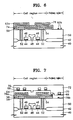
- FIG. 6 is a sectional view for illustrating a manufacturing method of the semiconductor memory device according to a second embodiment; and
- FIG. 7 is a sectional view for illustrating a manufacturing method of the semiconductor memory device according to a third embodiment.
- Referring to FIG. 4,
reference numeral 40 denotes a semiconductor substrate,reference numeral 42 denotes a field oxide film for defining an active region and a non-active region,reference numeral 44 denotes a gate insulating film of an oxide film, a nitride film or an ONO film,reference numeral 46 denotes a gate of polysilicon or polycide,reference numeral 48 denotes a bit line connected to a drain of a transistor (not shown),reference numerals reference numeral 52 denotes a plug for connecting a lower electrode of a capacitor to a source of the transistor (not shown),reference numeral 54 denotes a lower electrode of the capacitor,reference numeral 56 denotes a dielectric film,reference numeral 58 denotes an upper electrode of the capacitor,reference numeral 62a denotes a first material layer formed of a semiconductor or an insulator,reference numeral 62b denotes a resistor of a periphery region formed of a semiconductor or an insulator,reference numeral 68 denotes a barrier layer,reference numeral 70 denotes an interconnection layer andreference numeral 72 denotes a protective film. - On the semiconductor substrate, a capacitor having ferroelectric material including the
lower electrode 54, thedielectric film 56 and theupper electrode 58, the upper andlower electrodes - The
dielectric film 56 is formed of one selected from the group consisting of an oxide having a Perovskite structure such as PZT, PbTiO3, PbLaTiO3, BaTiO3, BaSrTiO3 and SrTiO3 or Bi4Ti3O12 and SrBi2Ta2O9. - On the
upper electrode 58,first material layers first material layers - In the case that the
first material layers interconnection layer 70 of a cell region to the first material layer thereof may be formed directly on a surface of thefirst material layer 62a. Here, in order to prevent mutual reaction and to form ohmic contact between thefirst material layer 62a and theinterconnection layer 70, preferably, afirst barrier layer 68 can be further included. Thefirst barrier layer 68 is formed of one selected from the group consisting of a double film of Ti/TiN, TiSixNy, TaSixNy, Ir and IrO2. - Also, as shown in FIG. 6, between the upper electrode 74 and the
first material layer 62a of the cell region, asecond barrier layer 76 for preventing mutual reaction of the upper electrode and the first material layer may be further included. Thesecond barrier layer 76 can be formed of the same material as that of thefirst barrier layer 68. - In FIG. 7,
first material layers upper electrode 58 and aninterconnection layer 70 can be formed of an insulator instead of a semiconductor such as polysilicon. - In the semiconductor memory device of the present invention, the first material layer formed of a semiconductor or an insulator having sheet resistance, which can be used for a resistor of a periphery region, is further included between the upper electrode of the capacitor having ferroelectric material and the interconnection layer. Thus, the adhesion of the interconnection layer to the upper electrode of the capacitor can be enhanced, and the first material layer can form the resistor of the periphery region.
- FIG. 5A shows the step of forming a transistor and a contact hole.
- The step is performed by forming an isolation film for isolating a semiconductor substrate into an active region and a non-active region, forming a transistor at the active region of the semiconductor substrate, forming a bitline connected to a drain of the transistor, forming an interlayer insulating film on the resultant structure where the bitline is formed, and forming a plug for connecting a source of the transistor and a lower electrode of the capacitor.
- In detail, a
field oxide film 42 is formed on asemiconductor substrate 40 using a typical isolation process such as local oxidation of silicon (LOCOS), and then a transistor having agate insulating film 44, agate electrode 46 and a source/drain (not shown) are formed in a usual manner. Subsequently, abitline 48 contacting the drain of the transistor is formed, and then an insulating film is deposited on the entire surface of the resultant structure where thebitline 48 is formed, to thereby form aninterlayer insulating film 50. Then, theinterlayer insulating film 50 is partially etched, to thereby form a contact hole. The contact hole is filled with conductive material, to thereby form aplug 52 for connecting a source of the transistor to the lower electrode of the capacitor. - FIG. 5B shows the step of forming
lower electrode 54 of the capacitor. - The step is performed by depositing a platinum group metal or a conductive oxide, thereby forming a conductive layer, and patterning the conductive layer.
- In detail, conductive material for forming the lower electrode of the capacitor on the resultant structure, where the
plug 52 is formed, is deposited to a thickness of approximately 100 ~ 3,000Å, to thereby form a conductive layer. Then, the conductive layer is patterned using a conventional photolithography method, to thereby form thelower electrode 54 of the capacitor. - The material for forming the
lower electrode 54 of the capacitor is, one selected from the group consisting of a conductive material having high conductivity and oxidation-resistance such as Pt, Ru, Ir, Pd or Os, a conductive oxide such as IrO2, platinum oxide (PtO), Osmium oxide (OsO2) Indium oxide (In2O3), Indium Tin Oxide (ITO), RuO2, and a combination of the conductive material with the conductive oxide. - A sputtering or chemical vapor deposition (CVD) is used to deposit the electrode material. For example, in order to deposit a platinum metal group by sputtering, the metal is used as a target under an argon (Ar) atmosphere, at a substrate temperature of 20 ~ 500°C and at a chamber pressure of 1 ~ 10mTorr. To deposit a platinum group metal oxide by radio frequency (RF) sputtering or reactive sputtering, the metal is used as a target under an atmosphere of mixed gases of Ar with O2 of 5 ~ 50% and further, at a chamber pressure of 1 ~ 10mTorr. To deposit platinum by a CVD method, platinum-hexafluoroacetyl acetonate (Pt-HFA)2 is used as a platinum source. Here, Ar of 100 ~ 1,000sccm is provided at a chamber pressure of 10mTorr ~ 10Torr and at substrate temperature of 100 ~ 500°C.
- FIG. 5C shows the step of forming a
dielectric film 56 and aconductive layer 58 for an upper electrode of a capacitor. - The step is performed by depositing ferroelectric material on the resultant structure of FIG. 5B, thereby forming a dielectric film, and depositing a platinum group metal or a platinum oxide, thereby forming a conductive layer.
- In detail, ferroelectric material such as PZT, is deposited on the resultant structure where a lower electrode of the capacitor is formed, by sputtering or CVD, thereby forming the
dielectric film 56. Then, a platinum group metal or a conductive oxide, is deposited on the dielectric film in the same manner as that for forming thelower electrode 54, to thereby form theconductive layer 58 for an upper electrode. - The material for forming the
dielectric film 56, one selected from the group consisting of an oxide having a Perovskite structure such as PZT, PbTiO3, PbLaTiO3, BaTiO3, BST (BaSrTiO3) and STO (SrTiO3) or Bi4Ti3O12, SrBi2Ta2O9 can be used. - For example, in order to deposit the BST by sputtering, BST is used as a target under Ar and O2 atmosphere. Here, a substrate temperature of 450 ~ 650°C and a chamber pressure of 1 ~ 10mTorr are maintained. In order to deposit the BST by CVD, Ba(DPM)2, Sr(DPM)2 or Ti(DPM)2 is used as a main component of the CVD source and an oxide gas including O2_and N2O of 10 ~ 50% with Ar is provided into the chamber, in which the substrate temperature is 450 ~ 800°C and the chamber pressure is 0.1 ~ 10Torr.
- FIG. 5D shows the step of photolithography for patterning the
conductive layer 58 for an upper electrode. - The step is performed by forming a photo resist pattern on the conductive layer for the upper electrode and patterning the conductive layer for the upper electrode and the dielectric film.
- In detail, a material such as a photo resist for forming a mask layer on the resultant structure, where the
conductive layer 58 is formed for the upper electrode, photo resist is spin-coated to a thickness of 0.5 - 5µm, and then the coated photo resist is exposed and developed, thereby forming a photo resistpattern 60 for exposing theconductive layer 58 for the upper electrode of the periphery region. - Then, the
conductive layer 58 for the upper electrode of the periphery region and thedielectric film 56 thereof are etched, using the photo resistpattern 60 as a mask. Here, theconductive layer 58 for the upper electrode can be etched by wet or dry etching. As the etchant, a mixture of HCl and HNO3 can be used for wet-etching, or a mixed gas of O2 and Cl2 can be used for the dry-etching. - FIG. 5E shows the step of forming a
first material layer 62. - The step is performed by removing the photo resist pattern and depositing polysilicon on the resultant structure where the photo resist pattern is removed.
- In detail, the photo resist pattern is eliminated, and then on the entire surface of the resultant structure of the cell region and the periphery region, a semiconductor or insulator such as polysilicon, which can be used as a resistor of the periphery region, is deposited, to thereby form the
first material layer 62. Thefirst material layer 62 can be used as a barrier layer for enhancing adhesion of the upper electrode to the interconnection layer in the cell region and can be used for a resistor in the periphery region. - In order to form a polysilicon film for the
first material layer 62, SiH4 or SiH2Cl2 is used as a source and a dopant source including PH3 is implanted into a chamber, and a CVD method is used at a substrate temperature of 550 ~ 750°C. - The thickness and doping concentration of the
polysilicon film 62 should be controlled appropriately such that the sheet resistance of the polysilicon film is 5 ~ 500 Ω/□, which is the sheet resistance Rs required for resistance of the periphery region. It is preferred that the thickness of the polysilicon film is approximately 100 ~ 3,000Å. Here, in order to obtain the appropriate sheet resistance, the doping concentration of the polysilicon film is controlled by adding a dopant into the chamber during a CVD process or depositing undoped polysilicon, and then performing ion-implantation or diffusion. - Here, silicide such as WSix TiSix, TiSixNy and TaSixNy or an insulating film such as SiN or Al2O3, instead of the
polysilicon film 62, can be used. - FIG. 5F shows the step of forming an
interlayer insulating film 64 and acontact hole 66. - The step is performed by patterning a polysilicon film, depositing an insulator on the patterned polysilicon, thereby forming the interlayer insulating film, and etching the interlayer insulating film, thereby forming a contact hole for connecting the upper electrode of the capacitor and the interconnection layer thereof.
- In detail, the first material layer is patterned by a conventional photolithography, to thereby form a first material layer pattern, which can be used for the
barrier layer 62a for enhancing adhesion of theupper electrode 58 of the capacitor to the interconnection layer thereof, and can be used for theresistor 62b having a predetermined resistance in the periphery region. Then, one selected from the group consisting of BPSG, PSG, SG, SOG, USG, and a combination thereof, is deposited on the resultant structure to a predetermined thickness of approximately 2,000 ~ 10,000Å, to thereby form aninterlayer insulating film 64. - Then, the
interlayer insulating film 64 is partially etched by photolithography, to thereby form acontact hole 66 for connecting the upper electrode of the capacitor to the interconnection layer thereof. Here, thecontact hole 66 can be formed, with a surface of thefirst material layer 62a exposed or with a surface of theupper electrode layer 58 portion under the first material layer exposed. - FIG. 5G shows the step of forming a
barrier layer 68, aninterconnection layer 70 and aprotective film 72. - The step is performed by forming the
barrier layer 68 on the resultant structure where the contact hole is formed, and depositing interconnection metal on the resultant structure, thereby forming theinterconnection layer 70, patterning the interconnection layer and the barrier layer, and forming theprotective film 72 on the resultant structure. - In detail, on the resultant structure where the contact hole is formed, a material selected from the group consisting of a double film of Ti/TiN, TiSixNy, TaSix4y, Ir and IrO2 is deposited to a thickness of 100 ~ 1,000Å, to thereby form the
barrier layer 68 for preventing mutual diffusion of thefirst material layer 62a and the interconnection layer and forming an ohmic contact between thefirst material layer 62a and the interconnection layer. Sequentially, on the resultant structure where the barrier layer is formed, a metal such as Aluminum for interconnection, is deposited to a thickness of approximately 3,000 ~ 10,000Å, and then thebarrier layer 68 and theinterconnection layer 70 are patterned by photolithography. Then, a process of forming theprotective layer 72 and a succeeding process are performed by a typical manufacturing process of a DRAM. - In this first embodiment, on the upper electrode layer of the capacitor having ferroelectric material, a resistor of the periphery region is deposited. Thus, the resistor of the periphery region can be concurrently formed during formation of the capacitor, and adhesion of the upper electrode layer to the interconnection layer is enhanced, and further reliability can be enhanced. Also, the first material layer prevents stress due to reaction with an interlayer insulating film to be deposited.
- Referring to FIG. 6, the corresponding material layers are denoted by reference numerals used in the first embodiment.
- The second embodiment is suitable for preventing the mutual diffusion of an upper electrode of a capacitor and a first material layer, i.e., for forming the upper electrode by Pt.
- The manufacturing method of this embodiment involves the processes of forming a first barrier layer which is formed of Platinum on an upper electrode layer 74, forming the first material layer on the first barrier layer, exposing the first material layer of the periphery region by photolithography and patterning the first material layer, the first barrier layer and the upper electrode layer.
- In detail, by the same method as that of the first embodiment, a Platinum layer 74 is formed as a conductive layer for the upper electrode. Then, in order to prevent reaction of the Pt layer 74 and a
polysilicon film 62a formed at the first material layer, material for preventing reaction of Pt and polysilicon, i.e., TiN, Ir, IrO2, RuO2 or Ru, TiSixNy, TaSixNy is deposited on the platinum layer 74 to a thickness of 100 ~ 1,000Å by sputtering, to thereby form afirst barrier layer 76. Here, the processes of forming the polysilicon film, patterning the upper electrode layer, or forming a contact hole, which are performed by the same method as that in the first embodiment, will not be described. - According to the manufacturing method of a capacitor having ferroelectric material of the second embodiment, in addition to a first material layer, which is used for a resistor of a periphery region, a barrier layer for preventing the mutual reaction of the first material layer and the upper electrode layer is also formed, to thereby enhance reliability.
- Referring to FIG. 7, the corresponding material layers are denoted by reference numerals used in the first and second embodiments.
- The third embodiment is suitable for cases where an insulator instead of a semiconductor such as polysilicon is used as the
first material layers upper electrode 58 and theinterconnection layer 70. Here, the insulator is SiO2, Al2 O3 or SiN. Other processes performed by the same method as that in the first embodiment will not be described. However, in the case where the insulator instead of the semiconductor is used, as shown in FIG. 7, a contact hole for connecting the interconnection layers 68 and 70 to theupper electrode 58 in a cell region, is formed by etching theinsulator layer 78a to expose a surface of theupper electrode 58. - In a semiconductor memory device having a capacitor including ferroelectric material in accordance with the present invention, a semiconductor layer or an insulator layer is deposited on the upper electrode of the capacitor. Accordingly, the semiconductor layer or the insulation layer can be used for a resistor of a periphery region without deterioration of capacitor characteristics, adhesion of the upper electrode to the interconnection layer can be enhanced, and adhesion of the upper electrode to a dielectric film is improved. Also, a layer without stress, which is caused by a reaction with the interlayer insulating film, is formed between the electrode and the interlayer insulating film, to thereby prevent deterioration of capacitance in a subsequent process.
Claims (24)
- A semiconductor memory device comprising:a lower electrode (54) formed on a semiconductor substrate (40);a dielectric film (56) formed on the lower electrode (54) ;an upper electrode (58) formed on the dielectric film (56); anda first material layer (62a,62b) formed on the upper electrode and used as a resistor of a periphery region.
- A semiconductor memory device according to claim 1, wherein the upper electrode (58) and lower electrode (54) are formed from a material selected from the group consisting of a platinum group metal and conductive oxide.
- A semiconductor memory according to claim 2, wherein the platinum group metal is one selected from the group consisting of Pt, Ru, Ir, Pd and Os.
- A semiconductor memory according to claim 2, wherein the conductive oxide is one selected from the group consisting of IrO2, platinum oxide, Osmium oxide, Indium oxide, Indium Tin Oxide (ITO) and RuO2.
- A semiconductor memory device according to any preceding claim, wherein the dielectric film (56) is formed from a material selected from the group consisting of an oxide having Perovskite structure, Bi4Ti3O12 and SrBi2Ta2O9.
- A semiconductor memory device according to claim 5, wherein the oxide having Perovskite structure is one selected from the group consisting of PZT, PbTiO3, PbLaTiO3, BaTiO3, BST (BaSrTiO3) and STO (SrTiO3).
- A semiconductor memory device according to any preceding claim, wherein the first material layer (62a,62b) has sheet resistance of 5 ~ 500 Ω/□.
- A semiconductor memory device according to any preceding claim, wherein the first material layer (62a,62b) is formed from a material selected from the group consisting of polysilicon, tungsten silicide, SiN, Al2O3, TiSixNy and TaSixNy.
- A semiconductor memory device according to any preceding claim, further comprising a first barrier layer (68) and an interconnection layer (70) on the first barrier layer (68), wherein the first barrier layer (68) prevents reaction of the first material layer (62a,62b) and the interconnection layer (70).
- A semiconductor memory device according to claim 9, wherein the first barrier layer (68) is formed from a material selected from the group consisting of a double film of Ti/TiN, Ir, Ru, RuO2, TiSixNy, TaSixNy and IrO2.
- A semiconductor memory device according to claim 9 or 10, further comprising a second barrier layer (76) for preventing reaction of the upper electrode (58) and first material layer (62a,62b) between the upper electrode (58) and first material layer (62a,62b).
- A semiconductor memory device according to claim 11, wherein the second barrier layer (76) is formed from a material selected from the group consisting of Ti/TiN, Ir, Ru, RuO2, TiSixNy, TaSixNy and IrO2.
- A method of manufacturing a semiconductor memory device, comprising the steps of:forming a lower electrode on a semiconductor substrate;forming a dielectric film on the lower electrode;forming a conductive layer for an upper electrode on the dielectric film;patterning the conductive layer for the upper electrode and the dielectric film;forming a first material layer capable of being used as a resistor of a periphery region on the resultant structure;forming an interlayer insulating film on the resultant structure first material layer and then patterning, to form a contact hole which exposes a portion of the upper electrode; andforming an interconnection layer on the resultant structure where the contact hole is formed.
- A method according to claim 13, wherein the upper and lower electrodes are formed from a material selected from the group consisting of a platinum group metal and a conductive oxide.
- A method according to claim 14, wherein the platinum metal is one selected from the group consisting of Pt, Ru, Ir, Pd and Os.
- A method according to claim 14 or 15, wherein the conductive oxide is one selected from the group consisting of IrO2, platinum oxide, Osmium oxide, Indium oxide, Indium Tin Oxide (ITO) and RuO2.
- A method according to any of claims 13 to 16, wherein the dielectric film is formed from a material selected from the group consisting of an oxide having Perovskite structure, Bi4Ti3O12 and SrBi2Ta2O9.
- A method according to claim 17, wherein the oxide having Perovskite structure is one selected from the group consisting of PZT, PbTiO3, PbLaTiO3, BaTiO3, BST (BaSrTiO3) and STO (SrTiO3).
- A method according to any of claims 13 to 18, wherein the first material layer is formed from a material having a sheet resistance of 5 ~ 500 Ω/□.
- A method according to any of claims 13 to 19, wherein the first material layer is formed of one selected from the group consisting of polysilicon, tungsten silicide, SiN, TiSixNy, TaSixNy and Al2O3.
- A method according to any of claims 13 to 20, further comprising the step of forming a first barrier layer on the first material layer for preventing reaction of the first material layer and interconnection layer, after the step of forming the first material layer.
- A method according to any of claims 13 to 21, wherein the first barrier layer is formed from a material selected from the group consisting of a double film of Ti/TiN, TisixNY, TaSixNy, Ir, IrO2, Ru and RuO2.
- A method according to any of claims 13 to 22, further comprising the step of forming a second barrier layer on the conductive layer for preventing reaction of the upper electrode and first material layer before the step of forming the first material layer.
- A method according to claim 23, wherein the second barrier layer is formed from a material selected from the group consisting of Ti/TiN, Ir, Ru, RuO2, TisixNy and TaSixNy.
Applications Claiming Priority (2)
| Application Number | Priority Date | Filing Date | Title |
|---|---|---|---|
| KR1019960021856A KR100234361B1 (en) | 1996-06-17 | 1996-06-17 | Semiconductor memory and its fabrication method having high dielectronic capacitor |
| KR9621856 | 1996-06-17 |
Publications (3)
| Publication Number | Publication Date |
|---|---|
| EP0814514A2 true EP0814514A2 (en) | 1997-12-29 |
| EP0814514A3 EP0814514A3 (en) | 1998-11-18 |
| EP0814514B1 EP0814514B1 (en) | 2002-08-14 |
Family
ID=19462163
Family Applications (1)
| Application Number | Title | Priority Date | Filing Date |
|---|---|---|---|
| EP97304161A Expired - Lifetime EP0814514B1 (en) | 1996-06-17 | 1997-06-13 | A semiconductor memory device including a capacitor |
Country Status (6)
| Country | Link |
|---|---|
| US (2) | US5955774A (en) |
| EP (1) | EP0814514B1 (en) |
| JP (1) | JP3955660B2 (en) |
| KR (1) | KR100234361B1 (en) |
| DE (1) | DE69714659T2 (en) |
| TW (1) | TW329037B (en) |
Cited By (3)
| Publication number | Priority date | Publication date | Assignee | Title |
|---|---|---|---|---|
| DE19845033A1 (en) * | 1998-09-30 | 2000-04-20 | Siemens Ag | Semiconductor device |
| WO2001075945A2 (en) * | 2000-04-03 | 2001-10-11 | Symetrix Corporation | Ferroelectric integrated circuit having hydrogen barrier layer |
| DE19825266B4 (en) * | 1997-06-19 | 2009-12-10 | LG Semicon Co., Ltd., Cheongju | A method of manufacturing a capacitor for a semiconductor device |
Families Citing this family (44)
| Publication number | Priority date | Publication date | Assignee | Title |
|---|---|---|---|---|
| EP0893832A3 (en) * | 1997-07-24 | 1999-11-03 | Matsushita Electronics Corporation | Semiconductor device including a capacitor device and method for fabricating the same |
| US6700145B1 (en) * | 1998-04-30 | 2004-03-02 | International Business Machines Corporation | Capacitor with high charge storage capacity |
| DE19857039A1 (en) * | 1998-12-10 | 2000-06-21 | Siemens Ag | Microelectronic structure |
| KR100324591B1 (en) * | 1998-12-24 | 2002-04-17 | 박종섭 | Method for forming capacitor by using TiAIN layer as diffusion barrier of top electrode |
| JP3539887B2 (en) * | 1999-04-09 | 2004-07-07 | 沖電気工業株式会社 | Semiconductor device and manufacturing method thereof |
| EP1067605A1 (en) * | 1999-07-05 | 2001-01-10 | STMicroelectronics S.r.l. | Ferroelectric memory cell and corresponding manufacturing method |
| JP2001057412A (en) * | 1999-08-19 | 2001-02-27 | Mitsubishi Electric Corp | Semiconductor device and manufacture thereof |
| KR100343287B1 (en) * | 1999-09-21 | 2002-07-15 | 윤종용 | Method for fabricating a high density ferroelectric memory device |
| DE19950540B4 (en) * | 1999-10-20 | 2005-07-21 | Infineon Technologies Ag | Process for the preparation of a capacitor electrode with barrier structure |
| JP3505497B2 (en) * | 1999-11-17 | 2004-03-08 | 三洋電機株式会社 | Dielectric element |
| JP3464956B2 (en) * | 1999-12-09 | 2003-11-10 | Necエレクトロニクス株式会社 | Semiconductor device |
| KR100517911B1 (en) * | 2000-05-19 | 2005-10-04 | 주식회사 하이닉스반도체 | Semiconductor fabrication method capable of preventing misalign between bottom electrode and storage node contact and oxidation of diffusion barrier layer |
| JP4286439B2 (en) | 2000-08-11 | 2009-07-01 | 富士通マイクロエレクトロニクス株式会社 | Manufacturing method of semiconductor device |
| KR100396879B1 (en) | 2000-08-11 | 2003-09-02 | 삼성전자주식회사 | Semiconductor memory device having capacitor encapsulated by multi-layer which includes double layeres being made of same material and method of manufacturing thereof |
| US7327582B2 (en) * | 2000-09-21 | 2008-02-05 | Ultrasource, Inc. | Integrated thin film capacitor/inductor/interconnect system and method |
| US6737728B1 (en) * | 2000-10-12 | 2004-05-18 | Intel Corporation | On-chip decoupling capacitor and method of making same |
| JP2002151657A (en) | 2000-11-08 | 2002-05-24 | Sanyo Electric Co Ltd | Dielectric element and manufacturing method therefor |
| JP2002231903A (en) | 2001-02-06 | 2002-08-16 | Sanyo Electric Co Ltd | Dielectric element and method of manufacturing the same |
| JP2004523924A (en) * | 2001-03-21 | 2004-08-05 | コーニンクレッカ フィリップス エレクトロニクス エヌ ヴィ | Electronic device |
| JP3892736B2 (en) * | 2001-03-29 | 2007-03-14 | 株式会社東芝 | Semiconductor memory device |
| US7084080B2 (en) * | 2001-03-30 | 2006-08-01 | Advanced Technology Materials, Inc. | Silicon source reagent compositions, and method of making and using same for microelectronic device structure |
| US6900498B2 (en) * | 2001-05-08 | 2005-05-31 | Advanced Technology Materials, Inc. | Barrier structures for integration of high K oxides with Cu and Al electrodes |
| DE10125594A1 (en) * | 2001-05-25 | 2002-12-05 | Infineon Technologies Ag | Semiconductor memory device and method for its production |
| JP4428500B2 (en) * | 2001-07-13 | 2010-03-10 | 富士通マイクロエレクトロニクス株式会社 | Capacitor element and manufacturing method thereof |
| US6998696B2 (en) * | 2001-09-21 | 2006-02-14 | Casper Michael D | Integrated thin film capacitor/inductor/interconnect system and method |
| US7425877B2 (en) * | 2001-09-21 | 2008-09-16 | Ultrasource, Inc. | Lange coupler system and method |
| KR20030039893A (en) * | 2001-11-16 | 2003-05-22 | 주식회사 하이닉스반도체 | Capacitor in semiconductor device and the method for fabricating thereof |
| EP1511442B1 (en) * | 2002-06-12 | 2010-01-06 | Boston Scientific Limited | Medical slings |
| KR100449253B1 (en) * | 2002-07-16 | 2004-09-18 | 주식회사 하이닉스반도체 | Method For Manufacture The Capacitor |
| KR100866708B1 (en) * | 2002-07-18 | 2008-11-03 | 주식회사 하이닉스반도체 | Manufacturing method of semiconductor device |
| US7326979B2 (en) * | 2002-08-02 | 2008-02-05 | Unity Semiconductor Corporation | Resistive memory device with a treated interface |
| US6800890B1 (en) * | 2002-12-30 | 2004-10-05 | Infineon Technologies Aktiengesellschaft | Memory architecture with series grouped by cells |
| KR100587669B1 (en) * | 2003-10-29 | 2006-06-08 | 삼성전자주식회사 | Method for forming resistor for use in semiconductor device |
| JP2005217044A (en) * | 2004-01-28 | 2005-08-11 | Fujitsu Ltd | Semiconductor device and method for manufacturing the same |
| JP4904671B2 (en) | 2004-06-24 | 2012-03-28 | 日本電気株式会社 | SEMICONDUCTOR DEVICE, ITS MANUFACTURING METHOD, AND ELECTRONIC DEVICE |
| EP1624479A3 (en) * | 2004-08-05 | 2008-07-16 | Samsung Electronics Co, Ltd | Ferroelectric memory and ferroelectric capacitor with Ir-alloy electrode or Ru-alloy electrode and method of manufacturing same |
| JP4913994B2 (en) * | 2004-08-09 | 2012-04-11 | セイコーエプソン株式会社 | Ferroelectric capacitor, ferroelectric memory, ferroelectric capacitor manufacturing method, and ferroelectric memory manufacturing method |
| KR100696766B1 (en) * | 2004-12-29 | 2007-03-19 | 주식회사 하이닉스반도체 | Charge trap insulator memory device |
| DE102005017072A1 (en) * | 2004-12-29 | 2006-07-13 | Hynix Semiconductor Inc., Ichon | Charge trap insulator memory device, has float channel, where data are read based on different channel resistance induced to channel depending on polarity states of charges stored in insulator |
| JP2007067096A (en) * | 2005-08-30 | 2007-03-15 | Fujitsu Ltd | Semiconductor device |
| US7750173B2 (en) * | 2007-01-18 | 2010-07-06 | Advanced Technology Materials, Inc. | Tantalum amido-complexes with chelate ligands useful for CVD and ALD of TaN and Ta205 thin films |
| EP2477919B1 (en) | 2009-09-18 | 2015-06-17 | Assa Abloy AB | Card substrate rotator |
| CN109216360B (en) | 2017-07-07 | 2021-01-12 | 联华电子股份有限公司 | Semiconductor memory device with a plurality of memory cells |
| CN109427786B (en) | 2017-08-21 | 2021-08-17 | 联华电子股份有限公司 | Semiconductor memory device and manufacturing process thereof |
Citations (4)
| Publication number | Priority date | Publication date | Assignee | Title |
|---|---|---|---|---|
| EP0490240A2 (en) * | 1990-12-03 | 1992-06-17 | Micron Technology, Inc. | Ferroelectric capacitor and method for forming local interconnection |
| JPH0513676A (en) * | 1991-07-02 | 1993-01-22 | Toshiba Corp | Semiconductor device |
| US5475248A (en) * | 1990-09-28 | 1995-12-12 | Ramtron International Corporation | Semiconductor device with a conductive reaction-preventing film |
| EP0697720A1 (en) * | 1994-08-01 | 1996-02-21 | Texas Instruments Incorporated | A conductive amorphous-nitride barrier layer for high dielectric-constant material electrodes |
Family Cites Families (12)
| Publication number | Priority date | Publication date | Assignee | Title |
|---|---|---|---|---|
| JPH0685431B2 (en) * | 1985-06-10 | 1994-10-26 | 株式会社日立製作所 | Semiconductor device |
| US5005102A (en) * | 1989-06-20 | 1991-04-02 | Ramtron Corporation | Multilayer electrodes for integrated circuit capacitors |
| US4982309A (en) * | 1989-07-17 | 1991-01-01 | National Semiconductor Corporation | Electrodes for electrical ceramic oxide devices |
| JPH0629461A (en) * | 1992-07-08 | 1994-02-04 | Mitsubishi Electric Corp | Capacitor structure of semiconductor device and manufacture thereof |
| JPH06125057A (en) * | 1992-10-12 | 1994-05-06 | Olympus Optical Co Ltd | Semiconductor memory containing ferroelectric film |
| JPH0793969A (en) * | 1993-09-22 | 1995-04-07 | Olympus Optical Co Ltd | Ferroelectric capacitance element |
| JPH07111318A (en) * | 1993-10-12 | 1995-04-25 | Olympus Optical Co Ltd | Ferroelectric substance memory |
| JPH07161931A (en) * | 1993-12-02 | 1995-06-23 | Nec Corp | Manufacture of semiconductor device |
| JP2875733B2 (en) * | 1994-02-15 | 1999-03-31 | 松下電子工業株式会社 | Method for manufacturing semiconductor device |
| US5716875A (en) * | 1996-03-01 | 1998-02-10 | Motorola, Inc. | Method for making a ferroelectric device |
| US5990507A (en) * | 1996-07-09 | 1999-11-23 | Kabushiki Kaisha Toshiba | Semiconductor device having ferroelectric capacitor structures |
| JP3157734B2 (en) * | 1997-02-03 | 2001-04-16 | 松下電子工業株式会社 | Ferroelectric memory device and method of manufacturing the same |
-
1996
- 1996-06-17 KR KR1019960021856A patent/KR100234361B1/en not_active IP Right Cessation
-
1997
- 1997-06-10 TW TW086107955A patent/TW329037B/en not_active IP Right Cessation
- 1997-06-12 JP JP15559897A patent/JP3955660B2/en not_active Expired - Fee Related
- 1997-06-12 US US08/873,641 patent/US5955774A/en not_active Expired - Lifetime
- 1997-06-13 EP EP97304161A patent/EP0814514B1/en not_active Expired - Lifetime
- 1997-06-13 DE DE69714659T patent/DE69714659T2/en not_active Expired - Lifetime
-
1999
- 1999-07-22 US US09/358,668 patent/US6211005B1/en not_active Expired - Fee Related
Patent Citations (4)
| Publication number | Priority date | Publication date | Assignee | Title |
|---|---|---|---|---|
| US5475248A (en) * | 1990-09-28 | 1995-12-12 | Ramtron International Corporation | Semiconductor device with a conductive reaction-preventing film |
| EP0490240A2 (en) * | 1990-12-03 | 1992-06-17 | Micron Technology, Inc. | Ferroelectric capacitor and method for forming local interconnection |
| JPH0513676A (en) * | 1991-07-02 | 1993-01-22 | Toshiba Corp | Semiconductor device |
| EP0697720A1 (en) * | 1994-08-01 | 1996-02-21 | Texas Instruments Incorporated | A conductive amorphous-nitride barrier layer for high dielectric-constant material electrodes |
Non-Patent Citations (1)
| Title |
|---|
| PATENT ABSTRACTS OF JAPAN vol. 017, no. 276 (E-1372), 27 May 1993 & JP 05 013676 A (TOSHIBA CORP), 22 January 1993, * |
Cited By (4)
| Publication number | Priority date | Publication date | Assignee | Title |
|---|---|---|---|---|
| DE19825266B4 (en) * | 1997-06-19 | 2009-12-10 | LG Semicon Co., Ltd., Cheongju | A method of manufacturing a capacitor for a semiconductor device |
| DE19845033A1 (en) * | 1998-09-30 | 2000-04-20 | Siemens Ag | Semiconductor device |
| WO2001075945A2 (en) * | 2000-04-03 | 2001-10-11 | Symetrix Corporation | Ferroelectric integrated circuit having hydrogen barrier layer |
| WO2001075945A3 (en) * | 2000-04-03 | 2002-01-31 | Symetrix Corp | Ferroelectric integrated circuit having hydrogen barrier layer |
Also Published As
| Publication number | Publication date |
|---|---|
| JP3955660B2 (en) | 2007-08-08 |
| US6211005B1 (en) | 2001-04-03 |
| DE69714659T2 (en) | 2003-04-10 |
| KR980006312A (en) | 1998-03-30 |
| DE69714659D1 (en) | 2002-09-19 |
| KR100234361B1 (en) | 1999-12-15 |
| US5955774A (en) | 1999-09-21 |
| TW329037B (en) | 1998-04-01 |
| JPH1056144A (en) | 1998-02-24 |
| EP0814514A3 (en) | 1998-11-18 |
| EP0814514B1 (en) | 2002-08-14 |
Similar Documents
| Publication | Publication Date | Title |
|---|---|---|
| EP0814514B1 (en) | A semiconductor memory device including a capacitor | |
| US5618746A (en) | Method for manufacturing a capacitor of semiconductor device having diffusion-blocking films | |
| US6930039B2 (en) | Method of fabricating a contact structure having a composite barrier layer between a platinum layer and a polysilicon plug | |
| US6078493A (en) | Fin-shaped capacitor | |
| JP3454058B2 (en) | Semiconductor memory and manufacturing method thereof | |
| US20010025976A1 (en) | Method for manufacturing a capacitor of a semiconductor device | |
| US7470595B2 (en) | Oxidizing a metal layer for a dielectric having a platinum electrode | |
| US6130124A (en) | Methods of forming capacitor electrodes having reduced susceptibility to oxidation | |
| US5742472A (en) | Stacked capacitors for integrated circuit devices and related methods | |
| US5861332A (en) | Method for fabricating capacitors of semiconductor devices | |
| US20030107076A1 (en) | Capacitor, method for fabricating the capacitor, and method for fabricating semiconductor device | |
| US6180970B1 (en) | Microelectronic devices including ferroelectric capacitors with lower electrodes extending into contact holes | |
| EP0847083B1 (en) | A method for manufacturing a capacitor for a semiconductor device | |
| US6534810B2 (en) | Semiconductor memory device having capacitor structure formed in proximity to corresponding transistor | |
| JPH1154703A (en) | Manufacture of high dielectric capacitor | |
| US20040147088A1 (en) | Capacitor | |
| US6306666B1 (en) | Method for fabricating ferroelectric memory device | |
| KR100652354B1 (en) | Capacitor of a semiconductor device having low contact resistance between a lower electrode and a contact plug and method for fabricating the same | |
| JPH09129849A (en) | Capacitor of semiconductor element and its preparation | |
| KR20010059002A (en) | A method for forming capacitor in semiconductor device | |
| KR100358163B1 (en) | Method for manufacturing ferroelectric memory device | |
| KR0168339B1 (en) | Capacitor fabrication method | |
| KR100200709B1 (en) | Ferroelectric capacitor of semiconductor device and method of manufacturing the same | |
| KR100866709B1 (en) | Manufacturing method for capacitor of semiconductor device | |
| KR20020008248A (en) | Method of ferroelectric memory device fabrication |
Legal Events
| Date | Code | Title | Description |
|---|---|---|---|
| PUAI | Public reference made under article 153(3) epc to a published international application that has entered the european phase |
Free format text: ORIGINAL CODE: 0009012 |
|
| AK | Designated contracting states |
Kind code of ref document: A2 Designated state(s): DE FR GB |
|
| 17P | Request for examination filed |
Effective date: 19980526 |
|
| PUAL | Search report despatched |
Free format text: ORIGINAL CODE: 0009013 |
|
| AK | Designated contracting states |
Kind code of ref document: A3 Designated state(s): AT BE CH DE DK ES FI FR GB GR IE IT LI LU MC NL PT SE |
|
| 17Q | First examination report despatched |
Effective date: 19990604 |
|
| AKX | Designation fees paid |
Free format text: DE FR GB |
|
| GRAG | Despatch of communication of intention to grant |
Free format text: ORIGINAL CODE: EPIDOS AGRA |
|
| GRAG | Despatch of communication of intention to grant |
Free format text: ORIGINAL CODE: EPIDOS AGRA |
|
| GRAH | Despatch of communication of intention to grant a patent |
Free format text: ORIGINAL CODE: EPIDOS IGRA |
|
| GRAH | Despatch of communication of intention to grant a patent |
Free format text: ORIGINAL CODE: EPIDOS IGRA |
|
| GRAA | (expected) grant |
Free format text: ORIGINAL CODE: 0009210 |
|
| AK | Designated contracting states |
Kind code of ref document: B1 Designated state(s): DE FR GB |
|
| REG | Reference to a national code |
Ref country code: GB Ref legal event code: FG4D |
|
| REF | Corresponds to: |
Ref document number: 69714659 Country of ref document: DE Date of ref document: 20020919 |
|
| ET | Fr: translation filed | ||
| PLBE | No opposition filed within time limit |
Free format text: ORIGINAL CODE: 0009261 |
|
| STAA | Information on the status of an ep patent application or granted ep patent |
Free format text: STATUS: NO OPPOSITION FILED WITHIN TIME LIMIT |
|
| 26N | No opposition filed |
Effective date: 20030515 |
|
| PGFP | Annual fee paid to national office [announced via postgrant information from national office to epo] |
Ref country code: DE Payment date: 20120524 Year of fee payment: 16 |
|
| PGFP | Annual fee paid to national office [announced via postgrant information from national office to epo] |
Ref country code: GB Payment date: 20120525 Year of fee payment: 16 Ref country code: FR Payment date: 20120705 Year of fee payment: 16 |
|
| GBPC | Gb: european patent ceased through non-payment of renewal fee |
Effective date: 20130613 |
|
| REG | Reference to a national code |
Ref country code: DE Ref legal event code: R119 Ref document number: 69714659 Country of ref document: DE Effective date: 20140101 |
|
| REG | Reference to a national code |
Ref country code: FR Ref legal event code: ST Effective date: 20140228 |
|
| PG25 | Lapsed in a contracting state [announced via postgrant information from national office to epo] |
Ref country code: GB Free format text: LAPSE BECAUSE OF NON-PAYMENT OF DUE FEES Effective date: 20130613 Ref country code: DE Free format text: LAPSE BECAUSE OF NON-PAYMENT OF DUE FEES Effective date: 20140101 |
|
| PG25 | Lapsed in a contracting state [announced via postgrant information from national office to epo] |
Ref country code: FR Free format text: LAPSE BECAUSE OF NON-PAYMENT OF DUE FEES Effective date: 20130701 |