EP0814382B1 - Improved photoresists and method for making printing plates - Google Patents
Improved photoresists and method for making printing plates Download PDFInfo
- Publication number
- EP0814382B1 EP0814382B1 EP97109966A EP97109966A EP0814382B1 EP 0814382 B1 EP0814382 B1 EP 0814382B1 EP 97109966 A EP97109966 A EP 97109966A EP 97109966 A EP97109966 A EP 97109966A EP 0814382 B1 EP0814382 B1 EP 0814382B1
- Authority
- EP
- European Patent Office
- Prior art keywords
- photoresist
- exposed
- substrate
- light
- layer
- Prior art date
- Legal status (The legal status is an assumption and is not a legal conclusion. Google has not performed a legal analysis and makes no representation as to the accuracy of the status listed.)
- Expired - Lifetime
Links
Images
Classifications
-
- G—PHYSICS
- G03—PHOTOGRAPHY; CINEMATOGRAPHY; ANALOGOUS TECHNIQUES USING WAVES OTHER THAN OPTICAL WAVES; ELECTROGRAPHY; HOLOGRAPHY
- G03F—PHOTOMECHANICAL PRODUCTION OF TEXTURED OR PATTERNED SURFACES, e.g. FOR PRINTING, FOR PROCESSING OF SEMICONDUCTOR DEVICES; MATERIALS THEREFOR; ORIGINALS THEREFOR; APPARATUS SPECIALLY ADAPTED THEREFOR
- G03F7/00—Photomechanical, e.g. photolithographic, production of textured or patterned surfaces, e.g. printing surfaces; Materials therefor, e.g. comprising photoresists; Apparatus specially adapted therefor
- G03F7/004—Photosensitive materials
- G03F7/008—Azides
-
- B—PERFORMING OPERATIONS; TRANSPORTING
- B41—PRINTING; LINING MACHINES; TYPEWRITERS; STAMPS
- B41C—PROCESSES FOR THE MANUFACTURE OR REPRODUCTION OF PRINTING SURFACES
- B41C1/00—Forme preparation
- B41C1/10—Forme preparation for lithographic printing; Master sheets for transferring a lithographic image to the forme
- B41C1/1008—Forme preparation for lithographic printing; Master sheets for transferring a lithographic image to the forme by removal or destruction of lithographic material on the lithographic support, e.g. by laser or spark ablation; by the use of materials rendered soluble or insoluble by heat exposure, e.g. by heat produced from a light to heat transforming system; by on-the-press exposure or on-the-press development, e.g. by the fountain of photolithographic materials
-
- C—CHEMISTRY; METALLURGY
- C07—ORGANIC CHEMISTRY
- C07C—ACYCLIC OR CARBOCYCLIC COMPOUNDS
- C07C247/00—Compounds containing azido groups
- C07C247/16—Compounds containing azido groups with azido groups bound to carbon atoms of six-membered aromatic rings of a carbon skeleton
- C07C247/18—Compounds containing azido groups with azido groups bound to carbon atoms of six-membered aromatic rings of a carbon skeleton being further substituted by carboxyl groups
-
- B—PERFORMING OPERATIONS; TRANSPORTING
- B41—PRINTING; LINING MACHINES; TYPEWRITERS; STAMPS
- B41C—PROCESSES FOR THE MANUFACTURE OR REPRODUCTION OF PRINTING SURFACES
- B41C2210/00—Preparation or type or constituents of the imaging layers, in relation to lithographic printing forme preparation
- B41C2210/02—Positive working, i.e. the exposed (imaged) areas are removed
-
- B—PERFORMING OPERATIONS; TRANSPORTING
- B41—PRINTING; LINING MACHINES; TYPEWRITERS; STAMPS
- B41C—PROCESSES FOR THE MANUFACTURE OR REPRODUCTION OF PRINTING SURFACES
- B41C2210/00—Preparation or type or constituents of the imaging layers, in relation to lithographic printing forme preparation
- B41C2210/10—Developable by an acidic solution
-
- B—PERFORMING OPERATIONS; TRANSPORTING
- B41—PRINTING; LINING MACHINES; TYPEWRITERS; STAMPS
- B41C—PROCESSES FOR THE MANUFACTURE OR REPRODUCTION OF PRINTING SURFACES
- B41C2210/00—Preparation or type or constituents of the imaging layers, in relation to lithographic printing forme preparation
- B41C2210/24—Preparation or type or constituents of the imaging layers, in relation to lithographic printing forme preparation characterised by a macromolecular compound or binder obtained by reactions involving carbon-to-carbon unsaturated bonds, e.g. acrylics, vinyl polymers
-
- Y—GENERAL TAGGING OF NEW TECHNOLOGICAL DEVELOPMENTS; GENERAL TAGGING OF CROSS-SECTIONAL TECHNOLOGIES SPANNING OVER SEVERAL SECTIONS OF THE IPC; TECHNICAL SUBJECTS COVERED BY FORMER USPC CROSS-REFERENCE ART COLLECTIONS [XRACs] AND DIGESTS
- Y10—TECHNICAL SUBJECTS COVERED BY FORMER USPC
- Y10S—TECHNICAL SUBJECTS COVERED BY FORMER USPC CROSS-REFERENCE ART COLLECTIONS [XRACs] AND DIGESTS
- Y10S430/00—Radiation imagery chemistry: process, composition, or product thereof
- Y10S430/145—Infrared
-
- Y—GENERAL TAGGING OF NEW TECHNOLOGICAL DEVELOPMENTS; GENERAL TAGGING OF CROSS-SECTIONAL TECHNOLOGIES SPANNING OVER SEVERAL SECTIONS OF THE IPC; TECHNICAL SUBJECTS COVERED BY FORMER USPC CROSS-REFERENCE ART COLLECTIONS [XRACs] AND DIGESTS
- Y10—TECHNICAL SUBJECTS COVERED BY FORMER USPC
- Y10S—TECHNICAL SUBJECTS COVERED BY FORMER USPC CROSS-REFERENCE ART COLLECTIONS [XRACs] AND DIGESTS
- Y10S430/00—Radiation imagery chemistry: process, composition, or product thereof
- Y10S430/146—Laser beam
Definitions
- This invention relates to improved positive photopolymer formulations and to their use in preparing printing plates. More particularly, this invention relates to the use of organoazide-containing photopolymer compositions for making printing plates.
- Photopolymers are used to make either positive-working or negative-working patterns on various substrates.
- Solventdevelopable photopolymers are a particular class of photopolymers that have the ability to either become more soluble, or less soluble, when exposed to light of a particular wavelength. Positive photopolymers become more soluble, and negative photopolymers become less soluble in a developer solution.
- a patterned mask After development of the resist with a solvent, a like or opposite pattern of the resist remains on the substrate.
- This developed or patterned photopolymer layer can then be used to prevent the action of a corrosive liquid or etchant (or etch gas when plasma etching is employed) from reacting with and removing portions of the substrate not protected by the photopolymer.
- Photopolymers or photoresists
- Photoresists have long been used in the semiconductor industry directly on semiconductor wafers to etch various features into the substrate. Resists are also used to make printed circuit boards wherein a conductive metal is deposited in photoresist openings to form printed circuits on the board substrate.
- resists are also used to form an image on a substrate, which is generally a metal plate.
- Ink is applied to the plate having a patterned photoresist layer thereon, and the ink can be transferred to another medium, such as paper. This process is well known.
- a photoresist is applied over the copper, and exposed to light of a desired frequency.
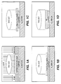
- the photoresist is covered with a patterned film emulsion or mask so that only certain areas of the photoresist are exposed, as shown in Fig. 1A, which illustrates a dot pattern.
- the photoresist is hardened or cross linked by the light, the film emulsion or mask is removed, and the plate is developed to solubilize the unexposed regions, as shown in Fig. 1B.
- the substrate is then etched, whereupon the exposed copper layer is removed, as shown in Fig. 1C.
- Ink is applied to the copper remaining on the aluminum plate in a press, and thereafter transferred to another substrate.
- the inked image is shown in Fig. 1D.
- the photoresist for such a system is important.
- the photoresist exposed to light must change its solubility between the exposed and non-exposed regions; it must be developable with standard solvents; and the insoluble portions must be insoluble enough so that they remain insoluble for a time sufficient to ensure that the soluble portions are completely removed during development, but that at least some thickness of the insoluble portions of the photoresist remain after development.
- a good photoresist for printing plates or other uses, such as for making printed circuit boards must be able to withstand attack by the etch solution used to etch the exposed portions of the substrate. These requirements are not trivial.
- positive photoresists comprise organo azide compounds mixed with a suitable filmforming polymeric resin, and a dye sensitive to a desired region of the spectrum. These ingredients can be admixed with suitable organic solvents to make a photoresist composition that is sensitive to laser light.
- the laser light must be able to be converted to heat energy by the dye, which is present in an amount sufficient to raise the temperature of the photoresist film above the decomposition temperature of the organo azide.
- the resist compositions of the invention can be patterned by direct application of computer controlled lasers to form finely controlled patterns.
- the unexposed portions of the resists cross link when flood exposed to ultraviolet (hereinafter UV) light, as from a UV lamp, which hardens the photoresists in those areas not already exposed to the laser light. This improves the solubility contrast between exposed and non-exposed areas of the resist.
- UV ultraviolet
- This hardening has another advantage also, in that it provides improved etch resistance for the patterned resist.
- the resist can be applied to a substrate and flood exposed prior to pattern exposure with laser light.
- the resist cross links and becomes hardened, so that it can be shipped for example prior to pattern exposure.
- an acid must be added to the developer solvent to solubilize the pattern exposed portions of the photoresist.
- the photoresists are useful to transfer patterns directly from a computer via a computer controlled light beam to a substrate such as a printing plate.
- Figs 1A, 1B, 1C and 1D illustrate the steps used to expose and form a pattern on a bimetal printing plate according to the prior art.
- the positive photoresists of the invention include an organo azide compound mixed with a suitable polymeric resin and a dye that is sensitive to light of a particular frequency, and that is also soluble in the photoresist solvent. Additional ingredients can be added, such as a pigment that can improve the contrast between the photoresist layer and an underlying substrate, and surfactants designed to adjust the texture of the photoresist so that it will form a smooth coating having a uniform thickness on a substrate. Typically lithographic photoresist films of this type have a dry thickness of about 0.5-2 micrometers. The above ingredients are then admixed with a suitable organic solvent so that it can be applied, as by spinning, as a thin film having a uniform thickness on the substrate. Generally the solids are dissolved to a total concentration of about 5% by weight in the mixed organic solvent.
- Polymeric resins suitable for use herein include polyvinyl formal resin, and polymers and copolymers of acrylates and methacrylates, styrene and the like,
- Suitable organo azide compounds are well known in the literature and are multifunctional, i.e., compounds having more than one azide group have been disclosed as negative, or cross linkable, resists.
- monofunctional azides which are not known to form cross linked negative photoresist patterns, are also suitable for use in the present invention.
- Suitable azides include monoaryl and vinyl azides, or bis arylazides, which may be substituted by various halogen and other radicals.
- Organoazides such as acidophthalic compounds that can form polymers are disclosed in US Patent 3,002,003 to Merrill et al for example. Cai et al, in Chem. Mater.
- organoazides are used together with dyes that are photosensitive to the frequency of the light emitted by the particular laser used for patterning the photoresist.
- the dye chosen for the present resists must be sensitive to the frequency of the laser used to expose the photoresist, and must be able to absorb the radiation from the laser and convert it to heat.
- Various dyes are well known and are available commercially that are sensitive to infrared light for example, having various emission frequency ranges.
- Merocyanine, cyanine and tricarbocyanine dyes are readily available infrared absorbing dyes.
- infrared lasers such as diode lasers, YAG lasers, carbon dioxide lasers and the like are readily available.
- lasers may be developed that lase in the visible light ranges as well. What is important here is that the dye be sensitive in the same region of the spectrum as the light emitted by the laser pattern light source.
- a flood exposure to ultra violet light can be made either before or after the pattern exposure by the laser.
- This flood exposure cross links the organo azides in the photoresist, hardening the photoresist.
- This cross linking reaction can also occur by heating the printing plate above about 150°C, e.g., to 160-180°C.
- the flood exposure method is presently preferred.
- a pigment can be dispersed in the photoresist solvent.
- a pigment can provide improved visual contrast between the photoresist film and the underlying substrate. This pigment may be insoluble, but must be dispersable in the photoresist solvent, and must be one that does not absorb light at the frequencies of the laser used to expose the photoresist. The pigment is added to provide additional contrast between the photoresist and the underlying substrate, so that it is more readily apparent when the development of the photoresist is complete.
- the photoresist compositions are made by mixing the resin, the organo azide and the laser sensitive dye together, and dissolving them in a suitable organic solvent. Generally the resist solution contains about 5% of solids. Additional ingredients can include surfactants, UV pigments as discussed above, coating agents and the like, as is known. For example fluorocarbon surfactants are known that are used in photoresists of various types.
- a first general process for making printing plates with the photoresists of the invention is detailed below.
- the resist layer formed in step A above can be flood exposed first, and then patterned with infrared light and developed afterwards.
- the photoresist is flood exposed with ultraviolet light that hardens the photoresist.
- the unpatterned plate can be shipped to a customer for pattern exposure with a computer controlled laser for example.
- this flood exposure makes the photoresist less susceptible to damage during shipping or transfer to the patterning site, and increases the contrast between pattern exposed and non-pattern exposed areas of the plate.
- the photoresist is then pattern exposed with laser light as before.
- the pattern exposed photoresist is then developed with a modified developer solution which contains an acid in addition to a conventional developer solution.
- a suitable developer solvent can include 0.9% by weight of hydroxyethane diphosphonic acid, 0.7% by weight of Avanel S74 surfactant, Avanel S74 is a tradename of PPG, Pittsburgh Plate Glass Industries, and 95% by weight of gamma-butyrolactone.
- the solution can contain up to about 3% by weight of water.
- the IR exposed regions of the photoresist become more soluble in the above developer solvent.
- Pentafluorobenzoic acid (21.2 gm or 0.1 mol) and 4.5 gm or 0.05 mol of butane diol were added to a 250 ml round bottom flask and purged with nitrogen.
- a solution of 1,3-dicyclohexylcarbodiimide of 100 mls of a 1 molar solution in methylene chloride was added and stirred for 24 hours and filtered.
- the resulting liquid was cooled to 5°C to produce a further precipitate, which was also removed by filtration.
- the compound was redissolved in acetone and 6.5 gm of sodium azide was added. This mixture was refluxed for 24 hours, filtered and the solvent evaporated to form a white solid. This solid was further purified by recrystallization from methanol.
- the resultant product had IR and NMR spectra consistent with the desired azide compound, including IR absorbance at 2132 cm -1 (azide) and 1724 cm -1 (ester carbonyl).
- Butane diol di(4-azidotetrafluorobenzoate) as prepared above was mixed with polyvinylformal and Projet 830 IR dye
- Projet 830 IR dye is a tradename of Avecia, Ltd. UK, an IR sensitive dye available from Zeneca Limited, varying the amount of the dye.
- a stock solution was prepared from the polyvinylformal in a mixture of 744 gm xylene, 396 gm dimethylacetamide and 0.296 grams of FC-431, a fluorocarbon surfactant commercially available from 3M Company. The fluoroazide was added and finally the IR dye.
- PVF polyvinyl formal: PVF, Parts Fluoroazide Projet 830 Total Solids 94.4 4.65 .96 15.575 94.19 4.64 1.28 15.625 93.8 4.63 1.59 15.675 93.5 4.61 1.91 15.725
- the coatings were spun at 60 rpm to form a photoresist film about 3.3 microns thick, and dried for 3 minutes at 110°C.
- the plates were exposed using a diode laser and by varying the amount of light, i.e., 150 mJ/cm 2 , 200 mJ/cm 2 , 300 mJ.cm 2 and 400 mJ/cm 2 to dot patterns varying from 3.1% to 96.9% patterns of dots about 10.6 ⁇ m in diameter.
- the plates were developed using PDI developer 181D. Clear images were observed in all cases.
- the plates were then etched with a copper etch, PDI's Q EtchTM solution.
- the plates were completely clean in the imaged areas and all copper was removed. There was no sign of attack in the non-imaged areas by the etchant.
- the remaining photoresist was removed by conventional photoresist stripping solutions.
- a photoresist formulation was prepared by mixing the following solids: 85.6 parts of polyvinyl formal resin; 5.2 parts of azido bis(2,6-benzylidine)cyclohexanone; 7.4 parts of Projet 830; 0.3 part of the surfactant FC-431; and 1.5 parts of phthalocyanine green pigment.
- the mixed solids were dissolved in a mixture of 66:33% of xylene and dimethylacetamide so as to make a 5% by weight solids solution, and coated on a copper clad aluminum bimetal printing substrate.
- the printing plate was exposed using a computer controlled diode laser that emits light having a frequency of 830 nm at a dose of 150 mJ/cm 2 , each laser flash delivered during a 3 microsecond period.
- the exposed plate was then flood exposed to UV light from a lamp.
- the printing plate was then developed using PDI's 181D developer solvent, a solution available from Printing Developments, Inc (hereinafter PDI), in a spray developer system.
- PDI Printing Developments, Inc
- the printing plate now had a patterned photoresist layer thereon wherein portions of the copper layer are exposed.
- the exposed copper was then etched down to the aluminum layer using a copper etchant PDI's "Q EtchTM” solution, a product of PDI.
- Example 2 The procedure of Example 2 was followed except varying the exposure of the photoresist to 150, 200, 300 and 400 mJ/cm 2 . Comparable results were obtained.
- Methyl 4-azidotetrafluorobenzoate was mixed with polyvinyl formal and Projet 830 IR dye as in Example 1.
- the coating solution was prepared by adding the azido benzoate to a suitable aliquot of the stock solution described in Example 1, such that the final solids contained 4.3% azidobenzoate, 2.0% Projet 830 and 92.7% of polyvinylformal.
- the above photoresist composition was applied to a printing plate, exposed and developed as in Example 1. Excellent results were obtained.
- a photoresist composition as described in Example 2 was applied to an aluminum substrate suitably treated to be hydrophilic as described for example in US Patent 3,181,461 to Fromson.
- the resulting polymer clad aluminum was exposed to high intensity laser light in a pattern, and developed as described in Example 3.
- Printer's ink applied concurrently with water adhered to the polymer image and avoided the exposed aluminum, non-image areas of the plate.
- Example 2 The procedure of Example 2 was followed except using a copper clad steel substrate. The resultant plate was exposed and developed as in Example 2, and the exposed copper was removed using PDI's "265E” bimetal etchant. Finally the remaining photopolymer was removed. Excellent results were obtained.
- a photopolymer composition was prepared as in Example 4 except using as the resin a copolymer of 50% benzyl methacrylate, 20% hydroxyethylmethacrylate, 20% methyl methacrylate and 10% allylmethacrylate prepared by solution polymerization of the corresponding monomers in 4-butyllactone at 55°C for 24 hours, using azobis(2-methylpropionitrile) as an initiator at a concentration of 12%.
- the formulation was coated, exposed, developed, etched and stripped as in Example 1. Excellent results were obtained.
- a photoresist composition was made containing 6 parts of 2,6-bis(4-azidobenzylidene)-4-methylcyclohexanone, 8 parts of Epolite III-178, an infrared absorbing dye made by Epolin Co., 1 part of Malachite Green Oxalate, a dye that absorbs visible light, 0.5 part of FC-431 surfactant, 1.5 parts of Chromadye 18 from Chroma Chemicals that changes color during pattern exposure to infrared light, and 84 parts of polyvinyl formal in a solvent of 50:50 xylene:dimethylacetamide (a solution containing 5% by weight of solids) was coated on a copper clad aluminum bimetal printing substrate as in Example 1. The resulting plate is subjected to an ultraviolet flood exposure of 400 mJ/cm 2 from a high pressure mercury arc lamp. The resulting plate can be exposed by a YAG laser exposure unit and processed as described hereinabove.
Landscapes
- Chemical & Material Sciences (AREA)
- Organic Chemistry (AREA)
- Physics & Mathematics (AREA)
- General Physics & Mathematics (AREA)
- Optics & Photonics (AREA)
- Thermal Sciences (AREA)
- Engineering & Computer Science (AREA)
- Manufacturing & Machinery (AREA)
- Photosensitive Polymer And Photoresist Processing (AREA)
- Exposure And Positioning Against Photoresist Photosensitive Materials (AREA)
- Manufacture Or Reproduction Of Printing Formes (AREA)
- Manufacturing Of Printed Circuit Boards (AREA)
Applications Claiming Priority (4)
| Application Number | Priority Date | Filing Date | Title |
|---|---|---|---|
| US873304 | 1992-04-24 | ||
| US08/666,169 US6037085A (en) | 1996-06-19 | 1996-06-19 | Photoresists and method for making printing plates |
| US666169 | 1996-06-19 | ||
| US08/873,304 US5962192A (en) | 1996-06-19 | 1997-06-11 | Photoresists and method for making printing plates |
Publications (2)
| Publication Number | Publication Date |
|---|---|
| EP0814382A1 EP0814382A1 (en) | 1997-12-29 |
| EP0814382B1 true EP0814382B1 (en) | 2001-11-28 |
Family
ID=27099397
Family Applications (1)
| Application Number | Title | Priority Date | Filing Date |
|---|---|---|---|
| EP97109966A Expired - Lifetime EP0814382B1 (en) | 1996-06-19 | 1997-06-18 | Improved photoresists and method for making printing plates |
Country Status (5)
| Country | Link |
|---|---|
| US (1) | US5962192A (ja) |
| EP (1) | EP0814382B1 (ja) |
| JP (1) | JPH10104829A (ja) |
| CA (1) | CA2207864C (ja) |
| DE (1) | DE69708515T2 (ja) |
Families Citing this family (22)
| Publication number | Priority date | Publication date | Assignee | Title |
|---|---|---|---|---|
| US6215269B1 (en) * | 1996-05-21 | 2001-04-10 | Kent Gregg | Method of exposing a path on a curved, or otherwise irregularly shaped, surface |
| US6664019B2 (en) * | 1996-06-19 | 2003-12-16 | Printing Developments Inc. | Aluminum printing plates and method of making |
| JP2000284506A (ja) * | 1999-03-31 | 2000-10-13 | Sharp Corp | フォトレジスト剥離剤組成物および剥離方法 |
| US6232031B1 (en) | 1999-11-08 | 2001-05-15 | Ano-Coil Corporation | Positive-working, infrared-sensitive lithographic printing plate and method of imaging |
| US7147338B2 (en) | 2001-04-09 | 2006-12-12 | Kent Gregg | Circuit on a curved, or otherwise irregularly shaped, surface, such as on a helmet to be worn on the head, including a fiber optic conductive path |
| US7008754B2 (en) | 2001-09-11 | 2006-03-07 | Daiken Chemical Co., Ltd. | Method for forming image on object surface including circuit substrate |
| DE60321148D1 (de) * | 2002-03-15 | 2008-07-03 | Kodak Graphic Comm Canada Co | Empfindlichkeitsverbesserung für strahlungsempfindliche elemente |
| US6843176B2 (en) * | 2002-04-26 | 2005-01-18 | Kodak Polychrome Graphics, Llc | Method to remove unwanted, unexposed, radiation-sensitive layer in a lithographic printing plate |
| US6924085B2 (en) * | 2003-03-18 | 2005-08-02 | Printing Developments, Inc. | Photoresist coatings for copper clad stainless steel printing plates |
| CN100380596C (zh) * | 2003-04-25 | 2008-04-09 | 株式会社半导体能源研究所 | 液滴排出装置、图案的形成方法及半导体装置的制造方法 |
| US7273773B2 (en) * | 2004-01-26 | 2007-09-25 | Semiconductor Energy Laboratory Co., Ltd. | Display device, method for manufacturing thereof, and television device |
| US7462514B2 (en) | 2004-03-03 | 2008-12-09 | Semiconductor Energy Laboratory Co., Ltd. | Semiconductor device and method for manufacturing the same, liquid crystal television, and EL television |
| US7642038B2 (en) * | 2004-03-24 | 2010-01-05 | Semiconductor Energy Laboratory Co., Ltd. | Method for forming pattern, thin film transistor, display device, method for manufacturing thereof, and television apparatus |
| US8158517B2 (en) * | 2004-06-28 | 2012-04-17 | Semiconductor Energy Laboratory Co., Ltd. | Method for manufacturing wiring substrate, thin film transistor, display device and television device |
| US20050287467A1 (en) * | 2004-06-29 | 2005-12-29 | Zaloom Jeffrey G | Enhanced durability printing plates and method of making |
| US20060216645A1 (en) * | 2005-03-22 | 2006-09-28 | Printing Developments, Inc. | Photoresist coatings for copper clad stainless steel printing plates |
| KR101102158B1 (ko) * | 2005-05-11 | 2012-01-02 | 삼성전자주식회사 | 신규한 유기 고분자 반도체, 이를 이용한 유기 고분자반도체 박막의 형성방법 및 이를 이용한 유기박막트랜지스터 |
| CA2511354A1 (en) * | 2005-07-04 | 2007-01-04 | National University Of Singapore | Radiation crosslinkers |
| US20080069858A1 (en) * | 2006-09-20 | 2008-03-20 | Boston Scientific Scimed, Inc. | Medical devices having biodegradable polymeric regions with overlying hard, thin layers |
| US20080274424A1 (en) | 2007-05-05 | 2008-11-06 | Yisong Yu | Positive photosensitive element comprising vinyl polymers |
| CN101762982B (zh) | 2008-12-24 | 2013-03-13 | 成都新图新材料股份有限公司 | 一种红外阳图热敏平版印刷版 |
| CN113016053A (zh) * | 2018-11-16 | 2021-06-22 | 朗姆研究公司 | 气泡缺陷减少 |
Family Cites Families (9)
| Publication number | Priority date | Publication date | Assignee | Title |
|---|---|---|---|---|
| US3864133A (en) * | 1970-08-11 | 1975-02-04 | Dainippon Ink & Chemicals | Photo-polymerizable compositions |
| US3958994A (en) * | 1974-08-26 | 1976-05-25 | American Hoechst Corporation | Photosensitive diazo steel lithoplate structure |
| JPS56132345A (en) * | 1980-03-21 | 1981-10-16 | Mitsubishi Chem Ind Ltd | Developer composition for lithographic plate |
| DE3417607A1 (de) * | 1983-05-12 | 1984-11-15 | Hitachi Chemical Co., Ltd. | Verfahren zur herstellung feiner muster |
| US4732840A (en) * | 1985-03-22 | 1988-03-22 | Fuji Photo Film Co., Ltd. | Planographic printing plate method using light sensitive material including phenolic resol with dibenzylic ether groups |
| DE3850533T2 (de) * | 1987-08-05 | 1994-10-27 | Ciba Geigy Ag | Bilderzeugungsverfahren. |
| DE3930087A1 (de) * | 1989-09-09 | 1991-03-14 | Hoechst Ag | Positiv arbeitendes strahlungsempfindliches gemisch und daraus hergestelltes strahlungsempfindliches aufzeichnungsmaterial |
| US5512418A (en) * | 1993-03-10 | 1996-04-30 | E. I. Du Pont De Nemours And Company | Infra-red sensitive aqueous wash-off photoimaging element |
| WO1996002021A1 (fr) * | 1994-07-11 | 1996-01-25 | Konica Corporation | Element initial pour plaque lithographique et procede de preparation de ladite plaque |
-
1997
- 1997-06-11 US US08/873,304 patent/US5962192A/en not_active Expired - Fee Related
- 1997-06-17 CA CA002207864A patent/CA2207864C/en not_active Expired - Fee Related
- 1997-06-18 JP JP9197687A patent/JPH10104829A/ja active Pending
- 1997-06-18 EP EP97109966A patent/EP0814382B1/en not_active Expired - Lifetime
- 1997-06-18 DE DE69708515T patent/DE69708515T2/de not_active Expired - Fee Related
Also Published As
| Publication number | Publication date |
|---|---|
| CA2207864C (en) | 2007-09-11 |
| CA2207864A1 (en) | 1997-12-19 |
| US5962192A (en) | 1999-10-05 |
| EP0814382A1 (en) | 1997-12-29 |
| DE69708515D1 (de) | 2002-01-10 |
| JPH10104829A (ja) | 1998-04-24 |
| DE69708515T2 (de) | 2002-07-11 |
Similar Documents
| Publication | Publication Date | Title |
|---|---|---|
| EP0814382B1 (en) | Improved photoresists and method for making printing plates | |
| EP1046958B1 (en) | Use of a composition for bottom reflection preventive film | |
| US6037085A (en) | Photoresists and method for making printing plates | |
| US6537735B1 (en) | Pattern-forming methods and radiation sensitive materials | |
| US5085972A (en) | Alkoxyalkyl ester solubility inhibitors for phenolic resins | |
| EP0633502B1 (en) | Pattern forming material | |
| JP3222459B2 (ja) | ポジ型フォトレジスト組成物 | |
| US20030087180A1 (en) | Photoresist composition for deep UV radiation containing an additive | |
| KR100694777B1 (ko) | 포토레지스트 조성물용 반사방지 코팅 | |
| EP1223470A1 (en) | Method for forming pattern | |
| EP0425142A2 (en) | Positive acting photoresist and method of producing same | |
| JPH07508840A (ja) | ポジ型放射線感応性混合物およびそれを使用して製造した記録材料 | |
| US5234791A (en) | Radiation-curable composition and radiation-sensitive recording material prepared therefrom for use with high-energy radiation | |
| EP0424124B1 (en) | Positive-acting photoresist compositions | |
| EP0778292A2 (en) | Method for the production of anhydride modified polyvinyl acetals useful for photosensitive compositions | |
| US5401608A (en) | Negative-working radiation-sensitive mixture and radiation-sensitive recording material produced therewith | |
| JPH08262717A (ja) | レジスト組成物及びレジストパターンの形成方法 | |
| DE4207264B4 (de) | Negativ arbeitendes strahlungsempfindliches Gemisch und damit hergestelltes Aufzeichnungsmaterial | |
| DE4002397A1 (de) | Strahlungsempfindliches gemisch und hieraus hergestelltes strahlungsempfindliches aufzeichnungsmaterial | |
| US4997748A (en) | Developer solution for positive-working resist composition | |
| DE69904223T2 (de) | Wasserlösliche positiv arbeitende photoresistzusammensetzung | |
| JPH03192260A (ja) | マレイミド含有陰画処理型深uvフォトレジスト | |
| EP1295177B1 (en) | Strongly water-soluble photoacid generator resist compositions | |
| Vollenbroek et al. | Photoresist systems for microlithography | |
| DE4338437C2 (de) | Lichtempfindliche Harzzusammensetzung |
Legal Events
| Date | Code | Title | Description |
|---|---|---|---|
| PUAI | Public reference made under article 153(3) epc to a published international application that has entered the european phase |
Free format text: ORIGINAL CODE: 0009012 |
|
| AK | Designated contracting states |
Kind code of ref document: A1 Designated state(s): DE DK FR GB IT NL SE |
|
| 17P | Request for examination filed |
Effective date: 19980527 |
|
| AKX | Designation fees paid |
Free format text: DE DK FR GB IT NL SE |
|
| RBV | Designated contracting states (corrected) |
Designated state(s): DE DK FR GB IT NL SE |
|
| 17Q | First examination report despatched |
Effective date: 19991111 |
|
| GRAG | Despatch of communication of intention to grant |
Free format text: ORIGINAL CODE: EPIDOS AGRA |
|
| GRAG | Despatch of communication of intention to grant |
Free format text: ORIGINAL CODE: EPIDOS AGRA |
|
| GRAH | Despatch of communication of intention to grant a patent |
Free format text: ORIGINAL CODE: EPIDOS IGRA |
|
| GRAH | Despatch of communication of intention to grant a patent |
Free format text: ORIGINAL CODE: EPIDOS IGRA |
|
| GRAA | (expected) grant |
Free format text: ORIGINAL CODE: 0009210 |
|
| AK | Designated contracting states |
Kind code of ref document: B1 Designated state(s): DE DK FR GB IT NL SE |
|
| PG25 | Lapsed in a contracting state [announced via postgrant information from national office to epo] |
Ref country code: NL Free format text: LAPSE BECAUSE OF FAILURE TO SUBMIT A TRANSLATION OF THE DESCRIPTION OR TO PAY THE FEE WITHIN THE PRESCRIBED TIME-LIMIT Effective date: 20011128 |
|
| REG | Reference to a national code |
Ref country code: GB Ref legal event code: IF02 |
|
| REF | Corresponds to: |
Ref document number: 69708515 Country of ref document: DE Date of ref document: 20020110 |
|
| PG25 | Lapsed in a contracting state [announced via postgrant information from national office to epo] |
Ref country code: SE Free format text: LAPSE BECAUSE OF FAILURE TO SUBMIT A TRANSLATION OF THE DESCRIPTION OR TO PAY THE FEE WITHIN THE PRESCRIBED TIME-LIMIT Effective date: 20020228 Ref country code: DK Free format text: LAPSE BECAUSE OF FAILURE TO SUBMIT A TRANSLATION OF THE DESCRIPTION OR TO PAY THE FEE WITHIN THE PRESCRIBED TIME-LIMIT Effective date: 20020228 |
|
| NLV1 | Nl: lapsed or annulled due to failure to fulfill the requirements of art. 29p and 29m of the patents act | ||
| PLBE | No opposition filed within time limit |
Free format text: ORIGINAL CODE: 0009261 |
|
| STAA | Information on the status of an ep patent application or granted ep patent |
Free format text: STATUS: NO OPPOSITION FILED WITHIN TIME LIMIT |
|
| 26N | No opposition filed | ||
| PGFP | Annual fee paid to national office [announced via postgrant information from national office to epo] |
Ref country code: DE Payment date: 20070801 Year of fee payment: 11 |
|
| PGFP | Annual fee paid to national office [announced via postgrant information from national office to epo] |
Ref country code: GB Payment date: 20070614 Year of fee payment: 11 |
|
| PGFP | Annual fee paid to national office [announced via postgrant information from national office to epo] |
Ref country code: IT Payment date: 20070614 Year of fee payment: 11 |
|
| PGFP | Annual fee paid to national office [announced via postgrant information from national office to epo] |
Ref country code: FR Payment date: 20070629 Year of fee payment: 11 |
|
| GBPC | Gb: european patent ceased through non-payment of renewal fee |
Effective date: 20080618 |
|
| REG | Reference to a national code |
Ref country code: FR Ref legal event code: ST Effective date: 20090228 |
|
| PG25 | Lapsed in a contracting state [announced via postgrant information from national office to epo] |
Ref country code: DE Free format text: LAPSE BECAUSE OF NON-PAYMENT OF DUE FEES Effective date: 20090101 |
|
| PG25 | Lapsed in a contracting state [announced via postgrant information from national office to epo] |
Ref country code: GB Free format text: LAPSE BECAUSE OF NON-PAYMENT OF DUE FEES Effective date: 20080618 |
|
| PG25 | Lapsed in a contracting state [announced via postgrant information from national office to epo] |
Ref country code: IT Free format text: LAPSE BECAUSE OF NON-PAYMENT OF DUE FEES Effective date: 20080618 Ref country code: FR Free format text: LAPSE BECAUSE OF NON-PAYMENT OF DUE FEES Effective date: 20080630 |