EP0811999A2 - Rastermikroskop - Google Patents
Rastermikroskop Download PDFInfo
- Publication number
- EP0811999A2 EP0811999A2 EP97108821A EP97108821A EP0811999A2 EP 0811999 A2 EP0811999 A2 EP 0811999A2 EP 97108821 A EP97108821 A EP 97108821A EP 97108821 A EP97108821 A EP 97108821A EP 0811999 A2 EP0811999 A2 EP 0811999A2
- Authority
- EP
- European Patent Office
- Prior art keywords
- scanning
- blocking
- charged particle
- particle beam
- light beam
- Prior art date
- Legal status (The legal status is an assumption and is not a legal conclusion. Google has not performed a legal analysis and makes no representation as to the accuracy of the status listed.)
- Granted
Links
Images


Classifications
-
- H—ELECTRICITY
- H01—ELECTRIC ELEMENTS
- H01J—ELECTRIC DISCHARGE TUBES OR DISCHARGE LAMPS
- H01J37/00—Discharge tubes with provision for introducing objects or material to be exposed to the discharge, e.g. for the purpose of examination or processing thereof
- H01J37/26—Electron or ion microscopes; Electron or ion diffraction tubes
- H01J37/28—Electron or ion microscopes; Electron or ion diffraction tubes with scanning beams
-
- G—PHYSICS
- G02—OPTICS
- G02B—OPTICAL ELEMENTS, SYSTEMS OR APPARATUS
- G02B21/00—Microscopes
- G02B21/0004—Microscopes specially adapted for specific applications
- G02B21/002—Scanning microscopes
-
- H—ELECTRICITY
- H01—ELECTRIC ELEMENTS
- H01J—ELECTRIC DISCHARGE TUBES OR DISCHARGE LAMPS
- H01J2237/00—Discharge tubes exposing object to beam, e.g. for analysis treatment, etching, imaging
- H01J2237/04—Means for controlling the discharge
- H01J2237/043—Beam blanking
-
- H—ELECTRICITY
- H01—ELECTRIC ELEMENTS
- H01J—ELECTRIC DISCHARGE TUBES OR DISCHARGE LAMPS
- H01J2237/00—Discharge tubes exposing object to beam, e.g. for analysis treatment, etching, imaging
- H01J2237/22—Treatment of data
Definitions
- the present invention relates to a scanning microscope in which a scanned image is obtained by scanning a charged particle beam or a light beam on a sample to be inspected, and more particularly to a scanning microscope which can reduce effects on the sample such as heating, contamination, charging-up by easily controlling intensity of the charged particle beam or the light beam to be scanned on the sample.
- an image can be obtained by scanning a charged particle beam or a light beam and detecting signals secondarily obtained there and then performing brightness modulation of a cathode-ray tube scanned in synchronism with the scanned charged particle beam or the scanned light beam.
- Intensity of the charged particle beam or the light beam to be irradiated on a sample is adjusted by taking effects on the sample such as temperature rising, contamination, charging-up into consideration.
- adjusting of the intensity has been performed by changing the conditions of the electron optical system forming an electron beam to be scanned such as quantity of electrons emitted from an electron source, condensing ratio, magnitude of aperture.
- the optical axis of the electron optical system will not stay in adjustment, i. e., will be shifted. Therefore, it has been required to adjust the optical axis again.
- An object of the present invention is to provide a scanning microscope in which intensity of electron beam irradiated on a sample can be easily changed without readjusting the optical axis.
- the present invention employs the following construction.
- the scanning microscope is provided a function to periodically blanking electron irradiation with setting a unit of two-dimensional scanning, and the average irradiated electron intensity is varied by changing the blanking ratio.
- the scanned image obtained here has flickers.
- the flickers in the scanned image due to blanking can be reduced as low as practically acceptable by setting the two-dimensional scanning frequency to the commercial television frequency and by accumulating and displaying the plurality of two-dimensional images.
- the present invention employs not a simple blanking but blanking by a two-dimensional scanning unit, it is easy to apply the present invention to the technology in which a sample image is obtained by accumulating scanned images.
- the present invention can be directly applied to the technology in which a sample image is obtained by accumulating a plurality of scanned images without complex calculating means.
- the same effect can be attained by superposing a blanking deflection signal to the voltage applied to the deflecting electrodes for two-dimensional scanning.
- FIG.1 is a diagram showing an embodiment of a scanning microscope in accordance with the present invention.
- FIG.2A to FIG.2D are charts explaining a method of displaying an accumulated image.
- FIG.3A to FIG.3D are charts explaining a method of displaying an accumulated image when blanking is performed.
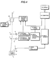
- FIG.4 is a diagram explaining another embodiment of a scanning microscope in accordance with the present invention in which a beam current is measured during blanking.
- FIG.5A and FIG.5B are views showing an example of display of beam currents which can be selected.
- FIG.6 is a block diagram explaining a conventional flow of a dimensional measurement process of a semiconductor wafer.
- FIG.7 is a block diagram explaining a flow of a dimensional measurement process in accordance with the present invention.
- FIG.1 shows an embodiment of a scanning microscope to which the present invention is applied.
- a finely focused electron beam 1 is performed two-dimensional scanning 5 on a sample 4 to be observed using a scanning deflection plate (Y) 2 and a scanning deflection plate (X) 3.
- a focusing system for focusing the electron beam 1 is not shown in the figure.
- the reference character 14 indicates an image memory which is, for example, of 512 ⁇ 512 pixels and has 256 levels of halftone in the depth direction.
- a write address generating circuit 12 is operated by a write clock 13 for a synchronizing signal. Speed of the write clock 13 determines one scanning time of the two-dimensional scanning.
- a cycle of the write clock 13 when a cycle of the write clock 13 is 60 ns, it becomes the TV scanning performing one two-dimensional scanning every 1/60 second.
- the cycle of the clock can be arbitrarily determined, and it is possible to construct a slow scanning system which scans one picture of image per one second.
- An address signal corresponding to a memory position of the image memory 14 is generated in the write address generating circuit 12 and is output to a Y-scanning D-A converter 9 and an X-scanning D-A converter 11.
- the address signal output to the X-scanning D-A converter 11 is a digital signal which repeats from 0 to 512, and is converted into an analog signal.
- the signal output to the Y-scanning D-A converter 9 is a digital signal which repeats from 0 to 512 and is added with one when the output of the X-scanning D-A converter 11 reaches 512 from 0, and is converted into an analog signal of saw-tooth shaped wave.
- These saw-tooth shaped wave analog signals are amplified with a Y-scanning amplifier 8 and an X-scanning amplifier 10, and are supplied to the scanning deflection plate (Y) 2 and the scanning deflection plate (X) 3. Size of the two-dimensional scanning 5 of the electron beam 1 on the sample 4 can be varied by changing amplification factors of the Y-scanning amplifier 8 and the X-scanning amplifier 10.
- secondary electrons 25 are emitted by the electron irradiation. Although reflected electrons and the like are also emitted, explanation here will be made with the secondary electrons as the typical electrons.
- the secondary electrons 25 are detected by a secondary electron detector 6, and the detected signal is converted to a digital signal by a signal A-D converter 7 to be stored in the image memory 14. Since an address of the image memory 14 is corresponds to an address scanned by the electron beam 1, a two-dimensional image of the two-dimensional scanning 5 in the sample 4 is stored in the image memory 14.
- the signals in the image memory 14 can be sequentially read in time sequence with a read address generating circuit 16 in synchronism with a read clock 17.
- the signals read out in corresponding with the address are converted from digital signals to analog signals by a signal D-A converter 15.
- the analog signals are used as a brightness modulation input to an image display cathode-ray tube 20.
- an address signal corresponding to the read address generating circuit 16 controlled by the read clock 17 is output to an X-deflecting D-A converter 18 and a Y-deflecting D-A converter 19 to be converted to voltages by an X-deflection amplifier 21 and a Y-deflection amplifier 22.
- the converted voltages are supplied to an X-deflection plate 23 and a Y-deflection plate 24 of the image display cathode-ray tube 20 to scan an electron beam of the cathode-ray tube in a rectangular shape.
- a distal signal read out of the image memory 14 by a read address signal is converted to an analog signal by the signal D-A converter 15 and is used as a brightness modulation input of the image display cathode-ray tube 20.
- a scanned image 26 of the sample 4 is displayed on the image display cathode-ray tube 20 as a scanned image 26.
- the speed of the read clock 17 is equal to the speed of the write clock 13.
- most of scanning electron microscopes in the past are of a slow speed scanning type having 10 seconds per one scanning, scanning electron microscopes having a faster scanning speed currently become dominant.
- One of the examples is a scanning electron microscope having one scanning time of 1/60 second as the TV frequency.
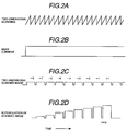
- FIG. 2A shows the feature of two-dimensional scanning which shows a saw-tooth shaped wave of Y-scanning.
- FIG.2B shows the feature of an electron beam irradiation on a sample, and the electrons are continuously irradiated.
- FIG.2C shows the feature forming a two-dimensional scanned image, and the two-dimensional scanned image is formed corresponding to two times of Y-scanning.
- FIG.2D shows the feature to perform accumulation of scanned images in order to improve the S/N ratio of the two-dimensional scanned image.
- the next two-dimensional scanning (+1) is executed, the two-dimensional scanned image (+1) is added and the two-dimensional scanned image (-8) is erased.
- the mean value in this explanation is an evenly averaged value of eight two-dimensional scanned images, it may be possible to employ a weighted arithmetic mean value in which the accumulated value of the two-dimensional scanned images from (-1) to (-8) is multiplied with 7/8 and then added with the next scanned image (+1).
- the present invention relates to a method of adjusting and controlling an irradiation intensity, that is, a beam current of the electron beam 1 on the sample 4 which is extremely effective when it is applied to a such scanning electron microscope performing observation of a sample, recording and capturing into a computer using an arithmetic mean value of two-dimensional scanned images.
- a blanking deflection plate 28 and a blanking aperture 29 are provided on the path of the electron beam 1.
- a blanking electric power source 27 generates a rectangular voltage in synchronism with the Y-scanning D-A converter to blank the electron beam 1 by a two-dimensional scanning unit. The blanking operation is controlled by the computer 30.
- FIG.3A shows the feature of two-dimensional scanning which shows the same saw-tooth shaped wave of Y-scanning as in FIG.2A.
- FIG.3B shows the feature of an electron beam irradiation on a sample which is controlled by blanking. In this example, blanking is performed every other two-dimensional scanning.
- FIG.3C shows the feature forming a two-dimensional scanned image.
- FIG.3D shows the state displaying an averaged image obtained by eight scanning operations through the arithmetic mean value processing of the two-dimensional scanned images.
- the processing is executed by averaging the images of eight scanning operations, but actually it is an averaged image obtained by four scanning times because the two-dimensional scanned image is formed every other scanning.
- the intensity of the accumulated image is reduced, but this problem can be solved by amplifying the signal depending on the degree of blanking.
- An observer hardly feels a sense of incongruity such as flickering when thinning-outs of the two-dimensional scanned images are within number of the arithmetic mean value processing operations (within the adding period). It must be noted here that the intensity of the electron beam (the beam current) becomes one-half of that in a continuous irradiation.
- the decrease in the intensity of the electron beam is not continuous but in average, the effect on the sample can be decreased to one-half.
- the beam current can be instantly changed at an arbitrary timing since the change can be performed only by blanking without changing the condition of the electron optical system.
- the cycle of blanking may be set equal to the cycle of arithmetic mean value processing, and the intensity can be varied within the range. For example, in a case where number of arithmetic mean value processing operations is 8, it is possible to adjust the beam current to eight levels of 1/8, 2/8, 3/8, 4/8, 5/8, 6/8, 7/8 and 8/8 (1.0).
- the present invention is also effective for confirming fluctuation in the beam current since the blanking is periodically performed.
- FIG.4 shows another embodiment of a scanning microscope in which a beam current is adjusted by actively making use of the present invention.
- the electron beam 1 deflected by the blanking deflection plate 28 enters into a blanking cup 31 having an opening in the central portion to be measured by a probe current meter 32 as the beam current.
- the current measurement is performed by applying a direct current voltage to the blanking deflection plate 28 for a certain time period based on a command from the computer and the measured beam current is stored in the computer.
- the measured beam current is used as a reference for the beam current. For example, when the measured value is 8 pA, the results may be displayed on the screen (display 32) of the computer as shown in FIG.5A to FIG.5B.
- FIG.5A shows a case where number of adding operations is 4 and it is possible to select 8, 6, 4 or 2 pA for the beam current.
- FIG.5B shows a case where number of adding operations is 8 and it is possible to select 8, 7, 6, 5, 4, 3, 2 or 1 pA for the beam current.
- the system is constructed to set the blanking condition to the selected one.
- the number of adding operations and the reducing ratio can be freely selected.
- the blanking ratio is selected from the displayed boxes. However, it is no need to say that the beam current value can be displayed by inputting a blanking ratio.
- number of blanking operations or amplification of the signal can be automatically set by setting a total value of accumulated beam current or a time period irradiated on the sample.
- the system of this type is effective for a case where it is empirically known what amount of beam irradiation may cause shape change or charging-up in an irradiated sample.
- number of adding operations and an amplification factor of the signal are set based on such an accumulative beam current value that the aforementioned trouble may not occur.
- the blanking electric power source further receives a long term blanking signal for blanking the electron beam 1 from the computer 30 at exchanging the sample and a blanking signal (A) for erasing a scan returning line.
- a long term blanking signal for blanking the electron beam 1 from the computer 30 at exchanging the sample
- a blanking signal (A) for erasing a scan returning line.
- the long term blanking and the returning line blanking signals are added through a circuital method, an electrode opposite to the blanking deflection plate 28 may be used.
- the blanking deflection plate 28 and the blanking cup 31 are provided in the aforementioned embodiment.
- One of the means is that the beam is turned aside from the two-dimensional scanning range of the sample using the scanning deflection plates 2 or 3. In order to do so, it is effective to provide a means for additionally applying such a high voltage to the scanning deflection plate that the beam may be deflected outside the two-dimensional scanning range of the sample at blanking timing.
- a very large effect can be attained when the present invention is applied to dimensional measurement in a semiconductor process.
- automatic operation of a scanning microscope without human operation becomes inevitable in order to improve through-put.
- FIG.6 shows a flow for performing dimensional measurement of a semiconductor wafer.
- a cassette containing 10 to 20 wafers to be measured is set to an automatic loader.
- the wafers contained in the cassette are successively extracted one-by-one by a transfer robot to be automatically loaded in an apparatus.
- an electron optical system is adjusted so as to agree to an electron beam condition suitable for observing the loaded wafer.
- energy of the electron beam is as low as nearly 800 V. Although the energy is changed depending on an observing condition in some cases, electron beam energy decreased up to 800 V is applicable to almost all kinds of semiconductor wafers. Therefore, the remaining condition to be set is the beam current condition.
- An intensity of beam current needs to be appropriately changed depending on a kind of wafer in order to suppress swelling change in measured dimensional value due to contamination, deformation due to heat and measuring error caused by deflection distortion due to charging-up.
- Setting the beam current requires operator s intervention and operating time of 10 to 20 minutes.
- the computer recognizes a position of the wafer by a specified point in the wafer, for example, a marker formed in the periphery of the wafer. By doing so, it is possible to observe and measure a specified arbitrary position. Measurement is performed by selecting specified chips (N) among several tens to several hundreds chips in the wafer and by successively moving specified points (n) in the specified chip.
- each of the N and the n is 5, and the total of 25 points are measured.
- the wafer is unloaded and the next wafer is loaded.
- Setting of the electron beam intensity is not necessary if the next wafer is to be observed under the completely same condition.
- the electron beam intensity is usually adjusted to a new appropriate condition. In this moment, it is required human intervention again.
- time required for adjustment becomes 200 to 400 minutes whereas it takes 30 minutes for loading and unloading and 30 minutes for actual measurement.
- the series of measuring operations cannot performed automatically without human intervention, which has hindered to realize an automated semiconductor process without human intervention.
- FIG.7 shows a flow of dimensional measurement process in accordance with the present invention.
- the electron optical system is adjusted using a test sample (for example, a mesh) prior to starting measurement.
- the electron beam is adjusted so as to obtain a necessary largest beam current under a continuous irradiation condition.
- a wafer is loaded and wafer alignment is performed.
- the electron beam is set to an observation condition of the wafer to be measured through beam current adjustment in accordance with the present invention.
- the wafer is automatically unloaded.
- wafer alignment is performed and an intensity of the electron beam is set.
- setting of the electron beam intensity can be completed within a fraction of a second whereas it has taken 10 to 20 minutes in the conventional system.
- it is possible to realize high speed and non-human-intervention measurement, wherein it takes 30 minutes for loading and unloading and 30 minutes for measurement.
- the means for adjusting electron optical system is designed so as to attain the effect of setting the irradiation intensity to an optimum value based on temperature rise of a sample, charging-up on an insulator and degree of contamination.
- the other conditions are set based on a beam current value and/or an accumulative added current value.
- Such an effect can be attained by constructing a scanning electron microscope so as to leave selection on which the priority is put, number of beam scanning operations, a beam current value or an accumulative added current value, to an operator in the process of the operator's intervention in the dimensional measurement flow described above.
- a display by which the operator can determine the selection on which the priority is put is displayed on the screen of the display unit 32. As the operator performs the selection, the condition put the priority is firstly determined and then the other conditions are manually or automatically determined based on the value.
- the method of the present invention it is possible to perform arbitrarily setting of an intensity of the electron beam (beam current) without performing the axial adjustment of the irradiation system which has been a problem on operation of a scanning electron microscope in the past, it is possible to set the irradiation intensity to an optimum value to temperature rise of a sample, charging-up on an insulator and degree of contamination which have been problems in the past, and accordingly it is possible to attain high speed and non-human intervention of automatic measurement in dimensional measurement of semiconductor wafers.
Landscapes
- Chemical & Material Sciences (AREA)
- Analytical Chemistry (AREA)
- Physics & Mathematics (AREA)
- General Physics & Mathematics (AREA)
- Optics & Photonics (AREA)
- Analysing Materials By The Use Of Radiation (AREA)
- Microscoopes, Condenser (AREA)
Applications Claiming Priority (3)
| Application Number | Priority Date | Filing Date | Title |
|---|---|---|---|
| JP14544796A JP3346172B2 (ja) | 1996-06-07 | 1996-06-07 | 走査形顕微鏡 |
| JP145447/96 | 1996-06-07 | ||
| JP14544796 | 1996-06-07 |
Publications (3)
| Publication Number | Publication Date |
|---|---|
| EP0811999A2 true EP0811999A2 (de) | 1997-12-10 |
| EP0811999A3 EP0811999A3 (de) | 2004-02-25 |
| EP0811999B1 EP0811999B1 (de) | 2014-07-09 |
Family
ID=15385442
Family Applications (1)
| Application Number | Title | Priority Date | Filing Date |
|---|---|---|---|
| EP97108821.6A Expired - Lifetime EP0811999B1 (de) | 1996-06-07 | 1997-06-02 | Rasterelektronenmikroskop |
Country Status (3)
| Country | Link |
|---|---|
| US (1) | US5929439A (de) |
| EP (1) | EP0811999B1 (de) |
| JP (1) | JP3346172B2 (de) |
Cited By (1)
| Publication number | Priority date | Publication date | Assignee | Title |
|---|---|---|---|---|
| EP1632980A3 (de) * | 2004-09-03 | 2008-07-23 | Carl Zeiss SMT Limited | Teilchenstrahl-Raster-Instrument |
Families Citing this family (12)
| Publication number | Priority date | Publication date | Assignee | Title |
|---|---|---|---|---|
| JP4434446B2 (ja) * | 2000-07-21 | 2010-03-17 | Okiセミコンダクタ株式会社 | 走査型電子顕微鏡の校正方法 |
| US7361894B2 (en) * | 2002-10-22 | 2008-04-22 | Hitachi High-Technologies Corporation | Method of forming a sample image and charged particle beam apparatus |
| EP1455378B1 (de) * | 2001-11-21 | 2013-08-14 | Hitachi High-Technologies Corporation | Probenabbildungsverfahren und system mit einem strahl geladener teilchen |
| US7349132B2 (en) * | 2003-01-30 | 2008-03-25 | Kabushiki Kaisha Toshiba | Image reading apparatus |
| CN1910725A (zh) * | 2004-01-14 | 2007-02-07 | 株式会社尼康 | 投射电子显微镜、电子显微镜、样品表面观察法和微器件制造法 |
| JP2006032613A (ja) * | 2004-07-15 | 2006-02-02 | Hitachi High-Technologies Corp | 電子ビーム電流計測方法、電子ビーム描画方法および装置 |
| JP2006242789A (ja) * | 2005-03-04 | 2006-09-14 | Fujitsu Ltd | 表面分析方法及び表面分析装置 |
| JP5022719B2 (ja) | 2007-01-30 | 2012-09-12 | 株式会社日立ハイテクノロジーズ | 荷電粒子線装置 |
| US8681068B1 (en) | 2009-09-15 | 2014-03-25 | Lockheed Martin Corporation | Highly agile wideband cavity impedance matching |
| WO2017090204A1 (ja) | 2015-11-27 | 2017-06-01 | 株式会社日立ハイテクノロジーズ | 荷電粒子線装置及び荷電粒子線装置における画像処理方法 |
| EP3538941B1 (de) | 2016-11-10 | 2025-04-23 | The Trustees of Columbia University in the City of New York | Schnelles hochauflösendes bildgebungsverfahren für grosse proben |
| DE102019107566A1 (de) * | 2019-03-25 | 2020-10-01 | Carl Zeiss Microscopy Gmbh | Verfahren zum Erzeugen eines Ergebnisbilds |
Citations (5)
| Publication number | Priority date | Publication date | Assignee | Title |
|---|---|---|---|---|
| US3628012A (en) | 1969-04-03 | 1971-12-14 | Graham Stuart Plows | Scanning stereoscopic electron microscope |
| US4713687A (en) | 1983-03-31 | 1987-12-15 | Research Development Corporation Of Japan | Scan line type dynamic observation apparatus |
| EP0533330A1 (de) | 1991-09-17 | 1993-03-24 | Hitachi, Ltd. | Rastermikroskop und Verfahren zur Bedienung eines solchen Rastermikroskops |
| JPH06301771A (ja) | 1993-04-13 | 1994-10-28 | Jeol Ltd | 画像信号積算装置 |
| US5500528A (en) | 1994-03-24 | 1996-03-19 | Nikon Corporation | Scanning electron microscope |
Family Cites Families (9)
| Publication number | Priority date | Publication date | Assignee | Title |
|---|---|---|---|---|
| JPS4814382B1 (de) * | 1969-03-17 | 1973-05-07 | ||
| US3714422A (en) * | 1970-04-06 | 1973-01-30 | Hitachi Ltd | Scanning stereoscopic electron microscope |
| GB1398513A (en) * | 1971-05-18 | 1975-06-25 | Drayton W B D | Electron probe instruments |
| JPS5565751U (de) * | 1978-10-31 | 1980-05-07 | ||
| JP2507290B2 (ja) * | 1983-12-14 | 1996-06-12 | 株式会社日立製作所 | ストロボ走査形電子顕微鏡 |
| JPS6187452U (de) * | 1984-11-14 | 1986-06-07 | ||
| JPH0618120B2 (ja) * | 1985-07-24 | 1994-03-09 | 株式会社日立製作所 | 荷電粒子ビーム装置 |
| JPH0820237B2 (ja) * | 1987-03-09 | 1996-03-04 | 株式会社日立製作所 | 電子顕微鏡用画像計測・検査装置 |
| JPH02295046A (ja) * | 1989-05-10 | 1990-12-05 | Hitachi Ltd | 論理解析電子ビームテスタ装置 |
-
1996
- 1996-06-07 JP JP14544796A patent/JP3346172B2/ja not_active Expired - Lifetime
-
1997
- 1997-06-02 EP EP97108821.6A patent/EP0811999B1/de not_active Expired - Lifetime
- 1997-06-04 US US08/868,650 patent/US5929439A/en not_active Expired - Lifetime
Patent Citations (5)
| Publication number | Priority date | Publication date | Assignee | Title |
|---|---|---|---|---|
| US3628012A (en) | 1969-04-03 | 1971-12-14 | Graham Stuart Plows | Scanning stereoscopic electron microscope |
| US4713687A (en) | 1983-03-31 | 1987-12-15 | Research Development Corporation Of Japan | Scan line type dynamic observation apparatus |
| EP0533330A1 (de) | 1991-09-17 | 1993-03-24 | Hitachi, Ltd. | Rastermikroskop und Verfahren zur Bedienung eines solchen Rastermikroskops |
| JPH06301771A (ja) | 1993-04-13 | 1994-10-28 | Jeol Ltd | 画像信号積算装置 |
| US5500528A (en) | 1994-03-24 | 1996-03-19 | Nikon Corporation | Scanning electron microscope |
Cited By (1)
| Publication number | Priority date | Publication date | Assignee | Title |
|---|---|---|---|---|
| EP1632980A3 (de) * | 2004-09-03 | 2008-07-23 | Carl Zeiss SMT Limited | Teilchenstrahl-Raster-Instrument |
Also Published As
| Publication number | Publication date |
|---|---|
| EP0811999A3 (de) | 2004-02-25 |
| JP3346172B2 (ja) | 2002-11-18 |
| JPH09330679A (ja) | 1997-12-22 |
| US5929439A (en) | 1999-07-27 |
| EP0811999B1 (de) | 2014-07-09 |
Similar Documents
| Publication | Publication Date | Title |
|---|---|---|
| US8604430B2 (en) | Method and an apparatus of an inspection system using an electron beam | |
| EP0949653B1 (de) | Elektronenstrahlgerät | |
| US5276325A (en) | Scanning microscope and a method of operating such a scanning microscope | |
| US7532328B2 (en) | Circuit-pattern inspection apparatus | |
| US5929439A (en) | Scanning microscope | |
| JP3934461B2 (ja) | 電子顕微鏡のチャージアップ防止方法および電子顕微鏡 | |
| JP2000208085A (ja) | 低電圧粒子ビ―ムを用いた半導体検査用の電圧コントラスト方法及び装置 | |
| US6365897B1 (en) | Electron beam type inspection device and method of making same | |
| US8086022B2 (en) | Electron beam inspection system and an image generation method for an electron beam inspection system | |
| US6815677B2 (en) | Scanning electron microscope and method of controlling the same | |
| JPH11242943A (ja) | 検査装置 | |
| JPH0729539A (ja) | 集束イオンビーム装置 | |
| JPH1050245A (ja) | 荷電粒子ビーム装置における焦点合わせ方法 | |
| JP4719699B2 (ja) | 走査型電子顕微鏡 | |
| JPH11283545A (ja) | 電子画像観察装置 | |
| JP2633861B2 (ja) | Sem式検査装置 | |
| JP3274650B2 (ja) | 走査電子顕微鏡 | |
| KR20240176566A (ko) | 기판 검사 방법 | |
| JPH02132741A (ja) | 電子線装置 | |
| JPH0935673A (ja) | 集束イオンビーム装置 | |
| JP2000082437A (ja) | 走査型荷電粒子ビーム装置 | |
| JPS61126752A (ja) | 走査形電子顕微鏡の偏向電源 |
Legal Events
| Date | Code | Title | Description |
|---|---|---|---|
| PUAI | Public reference made under article 153(3) epc to a published international application that has entered the european phase |
Free format text: ORIGINAL CODE: 0009012 |
|
| AK | Designated contracting states |
Kind code of ref document: A2 Designated state(s): AT BE CH DE DK ES FI FR GB GR IE IT LI LU MC NL PT SE |
|
| PUAL | Search report despatched |
Free format text: ORIGINAL CODE: 0009013 |
|
| RIC1 | Information provided on ipc code assigned before grant |
Ipc: 7G 02B 21/00 B Ipc: 7H 01J 37/28 A |
|
| AK | Designated contracting states |
Kind code of ref document: A3 Designated state(s): AT BE CH DE DK ES FI FR GB GR IE IT LI LU MC NL PT SE |
|
| 17P | Request for examination filed |
Effective date: 20040811 |
|
| AKX | Designation fees paid |
Designated state(s): DE GB NL |
|
| 17Q | First examination report despatched |
Effective date: 20050203 |
|
| GRAP | Despatch of communication of intention to grant a patent |
Free format text: ORIGINAL CODE: EPIDOSNIGR1 |
|
| RIC1 | Information provided on ipc code assigned before grant |
Ipc: H01J 37/28 20060101AFI20131113BHEP |
|
| INTG | Intention to grant announced |
Effective date: 20131211 |
|
| GRAS | Grant fee paid |
Free format text: ORIGINAL CODE: EPIDOSNIGR3 |
|
| GRAA | (expected) grant |
Free format text: ORIGINAL CODE: 0009210 |
|
| AK | Designated contracting states |
Kind code of ref document: B1 Designated state(s): DE GB NL |
|
| RAP1 | Party data changed (applicant data changed or rights of an application transferred) |
Owner name: HITACHI, LTD. |
|
| REG | Reference to a national code |
Ref country code: GB Ref legal event code: FG4D |
|
| REG | Reference to a national code |
Ref country code: DE Ref legal event code: R096 Ref document number: 69740721 Country of ref document: DE Effective date: 20140821 |
|
| REG | Reference to a national code |
Ref country code: NL Ref legal event code: VDEP Effective date: 20140709 |
|
| PG25 | Lapsed in a contracting state [announced via postgrant information from national office to epo] |
Ref country code: NL Free format text: LAPSE BECAUSE OF FAILURE TO SUBMIT A TRANSLATION OF THE DESCRIPTION OR TO PAY THE FEE WITHIN THE PRESCRIBED TIME-LIMIT Effective date: 20140709 |
|
| REG | Reference to a national code |
Ref country code: DE Ref legal event code: R097 Ref document number: 69740721 Country of ref document: DE |
|
| PLBE | No opposition filed within time limit |
Free format text: ORIGINAL CODE: 0009261 |
|
| STAA | Information on the status of an ep patent application or granted ep patent |
Free format text: STATUS: NO OPPOSITION FILED WITHIN TIME LIMIT |
|
| 26N | No opposition filed |
Effective date: 20150410 |
|
| GBPC | Gb: european patent ceased through non-payment of renewal fee |
Effective date: 20150602 |
|
| PG25 | Lapsed in a contracting state [announced via postgrant information from national office to epo] |
Ref country code: GB Free format text: LAPSE BECAUSE OF NON-PAYMENT OF DUE FEES Effective date: 20150602 |
|
| PGFP | Annual fee paid to national office [announced via postgrant information from national office to epo] |
Ref country code: DE Payment date: 20160524 Year of fee payment: 20 |
|
| REG | Reference to a national code |
Ref country code: DE Ref legal event code: R071 Ref document number: 69740721 Country of ref document: DE |