EP0809355A2 - Circuit amplificateur - Google Patents
Circuit amplificateur Download PDFInfo
- Publication number
- EP0809355A2 EP0809355A2 EP97108112A EP97108112A EP0809355A2 EP 0809355 A2 EP0809355 A2 EP 0809355A2 EP 97108112 A EP97108112 A EP 97108112A EP 97108112 A EP97108112 A EP 97108112A EP 0809355 A2 EP0809355 A2 EP 0809355A2
- Authority
- EP
- European Patent Office
- Prior art keywords
- amplifier
- transistor
- further transistor
- switched
- amplifier circuit
- Prior art date
- Legal status (The legal status is an assumption and is not a legal conclusion. Google has not performed a legal analysis and makes no representation as to the accuracy of the status listed.)
- Withdrawn
Links
- 238000012544 monitoring process Methods 0.000 claims description 4
- 230000003321 amplification Effects 0.000 description 1
- 239000003990 capacitor Substances 0.000 description 1
- 238000010586 diagram Methods 0.000 description 1
- 238000000034 method Methods 0.000 description 1
- 238000003199 nucleic acid amplification method Methods 0.000 description 1
- 238000013021 overheating Methods 0.000 description 1
- 230000000630 rising effect Effects 0.000 description 1
- 230000001629 suppression Effects 0.000 description 1
Images


Classifications
-
- H—ELECTRICITY
- H03—ELECTRONIC CIRCUITRY
- H03F—AMPLIFIERS
- H03F1/00—Details of amplifiers with only discharge tubes, only semiconductor devices or only unspecified devices as amplifying elements
- H03F1/30—Modifications of amplifiers to reduce influence of variations of temperature or supply voltage or other physical parameters
- H03F1/305—Modifications of amplifiers to reduce influence of variations of temperature or supply voltage or other physical parameters in case of switching on or off of a power supply
-
- H—ELECTRICITY
- H03—ELECTRONIC CIRCUITRY
- H03F—AMPLIFIERS
- H03F3/00—Amplifiers with only discharge tubes or only semiconductor devices as amplifying elements
- H03F3/20—Power amplifiers, e.g. Class B amplifiers, Class C amplifiers
- H03F3/21—Power amplifiers, e.g. Class B amplifiers, Class C amplifiers with semiconductor devices only
- H03F3/217—Class D power amplifiers; Switching amplifiers
- H03F3/2173—Class D power amplifiers; Switching amplifiers of the bridge type
Definitions
- the invention relates to an amplifier circuit with a plurality of output stage transistors which operate in the switch mode, and in particular to such an amplifier circuit for an LF amplifier.
- Amplifier output stages which work discontinuously in switch mode, can process much higher powers than in a constant amplifier mode. Rectangular pulses are amplified, which are pulse-width modulated, for example, and which are only demodulated after the final amplification and fed to a load.
- the invention has for its object to avoid abrupt changes in the output signal of such amplifiers when switching on or off in a simple and inexpensive manner.
- a single transistor is sufficient to effectively prevent, for example, switch-on and switch-off clicks.
- This transistor need only have a low permissible power loss, since loss conduction occurs only during switching on and off and also only for a very short time.
- the transistor can be turned on or off continuously with little effort, so that the cost of
- the embodiment of the invention is essentially limited to the cost of a single transistor.
- the presence of this transistor also opens up a possibility for measuring or monitoring the current through the loudspeaker coil.
- the invention is not only suitable for LF amplifiers with more or less directly connected loudspeakers, but also for the most varied amplifiers for pulse signals, which are subsequently converted into amplitude-analog signals, and for the most varied loads.
- the switch-on or switch-off pulses are effectively suppressed even when the amplifier is not a power amplifier, but rather an analog high-performance amplifier is connected to it.
- the term "output stage transistors" used here should therefore be understood to mean that these transistors form the last stage of an amplifier circuit, to which further circuits can also be connected.
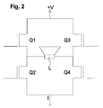
- LF amplifier output stages are usually designed as a half-bridge circuit, as shown in FIG. 1, or as a full-bridge circuit, as shown in FIG. 2.
- Fig. 1 two MOSFET transistors Q1 and Q2 are connected in series between a positive supply voltage V and ground, and a loudspeaker L is connected on one side to the source of transistor Q1 and the drain of transistor Q2 and on the other side to a supply voltage V / 2 connected.
- FIG. 2 four MOSFET transistors Q1 to Q4 are arranged in a bridge circuit between the positive supply voltage V and ground, with a loudspeaker L connected across as a load.
- the output stage transistors shown in Fig. 1 or Fig. 2 operate in switch mode, i.e. they are each either in the on or in the off state and output square-wave signals which are fed directly to the loudspeaker L.
- These square-wave signals have a repetition frequency that is significantly higher than the highest frequency that can be processed by the loudspeaker.
- pulse-width-modulated square-wave signals are provided, which are demodulated by the loudspeaker itself, since the loudspeaker cannot follow the square-wave signals directly, but adjusts itself to the mean value of a number of successive pulses, which corresponds to the instantaneous value of the signal amplitude.
- a separate demodulator can also be provided, for example a low-pass filter in the loudspeaker line.
- a current I suddenly flows through the speaker coil, which corresponds to the instantaneous value of the signal amplitude.
- FIG. 3 in which the current I increases from zero to a value at a switch-on instant t1, which corresponds to the instantaneous value of the signal amplitude.
- the time axis is shown in a very high time resolution so that the current value appears as a horizontal line (like a direct current) and subsequent changes in accordance with the instantaneous value of the signal amplitude are not visible in the diagram.
- the time span within which the current I through the loudspeaker coil increases from zero to the constant value shown is not zero, because of the short one Switching times of the transistors (typically in the range from 10 to 100 ns), however, are so short that an audible "click" is generated in the loudspeaker.
- the current I abruptly returns to zero from any instantaneous value (the same value is shown in FIG. 3 as when it was switched on).
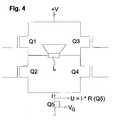
- a further MOSFET transistor Q5 is inserted into the line to ground in a circuit as in FIG. 2. As shown in Figure 4, the source of transistor Q5 is connected to ground and its drain is connected to the source of transistors Q2 and Q4.
- the control electrode or the gate of the transistor Q5 is driven by a control voltage V G , such that when the amplifier is switched on and off, instead of the current profile shown in FIG. 3, the current profile shown in FIG. 5 results through the loudspeaker coil.
- the current I through the loudspeaker coil does not suddenly increase at time t1, but gradually increases to the instantaneous value of the signal amplitude, and gradually goes back to zero at time t2.
- the rise and fall times of the current I through the loudspeaker coil are selected so that they are greater than the reciprocal lower listening frequency, ie greater than approx. 1/20 second, so that the loudspeaker does not produce any audible noise when the amplifier is switched on and off . Under certain circumstances, it may be sufficient to suppress only the switching noise when switching on or when switching off.
- the current profile shown in FIG. 5 is not only continuous, but also continuously differentiable, ie without any "kink".
- the rise and fall times of the current I through the loudspeaker coil do not have to be significantly greater than approximately 1/20 second in order to effectively prevent switch-on and switch-off clicks. If the rise and fall times are long enough, any steady course can suffice, for example, rising and falling edges with a constant slope.
- the control voltage V G can be taken, for example, from a capacitor which is charged by the power supply via a resistor when it is switched on and is discharged again when the power supply is switched off.
- the control voltage V G can also be generated by means of a digital logic circuit or an existing signal processor, so that one does not need any discrete components.
- both the transistor Q5 and the circuit for generating its control voltage V G can be included in an integrated circuit which forms the amplifier.
- the amplifier transistors Q1 to Q4 and transistor Q5, which operate in amplifier mode, are ideally suited for implementation within an integrated circuit due to their low power dissipation. This allows an extremely small and compact amplifier to be realized without a switch-on and switch-off crack, which can be accommodated, for example, in a loudspeaker chassis, so that a very compact active loudspeaker results, for example, for automobiles.
- the transistor Q5 is inserted in the ground line of the amplifier, but it can also be inserted in the line to the positive supply voltage V. Suppression of switch-on or switch-off clicks in the manner described can also be possible with other types of output stage circuits than shown in FIG. 4; it is essential that the further transistor is in the current path through the loudspeaker or another load. In the case of a half-bridge circuit as in FIG. 2, this further transistor could consist, for example, in a "double transistor" in the connecting line of the loudspeaker with the supply voltage V / 2, i.e. a component that can be blocked or made conductive in both directions at the same time. Accordingly, the term "transistor” used here is to be understood generally as a component whose conductivity can be changed continuously in either or in both directions.
- the output signal of the analog-digital converter can be processed by a signal processor or a logic circuit in order to continuously monitor the current I through the transistor Q5. If the current I exceeds a permissible value because of a short circuit at the output, the signal processor or the logic circuit can block the transistor Q5 extremely quickly in order to protect the transistors Q1 to Q4 if the signal processor or the logic circuit simultaneously generates the control current I, such as described above.
- the amplifier can also be monitored for other error levels, for example DC voltages at the loudspeaker connections or overheating conditions, to quickly block transistor Q5 to protect transistors Q1 to Q4 in the event of an error.
- error levels for example DC voltages at the loudspeaker connections or overheating conditions
- the monitoring of the current I and possibly other parameters can also be carried out in an analog manner or with conventional discrete components, but a digital monitoring circuit has the advantage that, like the circuit for generating the control voltage V G, it is easily integrated into an amplifier module can be.
Landscapes
- Engineering & Computer Science (AREA)
- Power Engineering (AREA)
- Amplifiers (AREA)
Applications Claiming Priority (2)
| Application Number | Priority Date | Filing Date | Title |
|---|---|---|---|
| DE19620693 | 1996-05-22 | ||
| DE1996120693 DE19620693C1 (de) | 1996-05-22 | 1996-05-22 | Verstärkerschaltung |
Publications (2)
| Publication Number | Publication Date |
|---|---|
| EP0809355A2 true EP0809355A2 (fr) | 1997-11-26 |
| EP0809355A3 EP0809355A3 (fr) | 1998-05-20 |
Family
ID=7795069
Family Applications (1)
| Application Number | Title | Priority Date | Filing Date |
|---|---|---|---|
| EP97108112A Withdrawn EP0809355A3 (fr) | 1996-05-22 | 1997-05-20 | Circuit amplificateur |
Country Status (2)
| Country | Link |
|---|---|
| EP (1) | EP0809355A3 (fr) |
| DE (1) | DE19620693C1 (fr) |
Cited By (1)
| Publication number | Priority date | Publication date | Assignee | Title |
|---|---|---|---|---|
| CN102324895A (zh) * | 2011-07-01 | 2012-01-18 | 四川和芯微电子股份有限公司 | Pop噪声抑制电路及方法 |
Families Citing this family (1)
| Publication number | Priority date | Publication date | Assignee | Title |
|---|---|---|---|---|
| DE19929841C2 (de) * | 1999-06-29 | 2001-07-12 | Jan Quellmann | Getakteter Verstärker, insbesondere zur Verstärkung von Audiosignalen |
Family Cites Families (6)
| Publication number | Priority date | Publication date | Assignee | Title |
|---|---|---|---|---|
| JPS57170606A (en) * | 1981-04-10 | 1982-10-20 | Sony Corp | Amplifying circuit for pulse-width-modulated signal |
| IT1215247B (it) * | 1985-03-13 | 1990-01-31 | Ates Componenti Elettron | Dispositivo e procedimento per azzerare un segnale di uscita in un amplificatore a commutazione. |
| DD265484A1 (de) * | 1987-10-06 | 1989-03-01 | Bitterfeld Braunkohle | Verstaerker hoher leistung |
| US5199079A (en) * | 1991-05-21 | 1993-03-30 | Thomson Consumer Electronics, Inc. | Supply voltage responsive audible transient (POP) suppression arrangement |
| JPH06152270A (ja) * | 1992-11-10 | 1994-05-31 | Fujitsu Ten Ltd | スイッチング増幅回路 |
| US5479134A (en) * | 1993-09-20 | 1995-12-26 | Rohm Co., Ltd. | Power amplifier circuit for audio signal and audio device using the same |
-
1996
- 1996-05-22 DE DE1996120693 patent/DE19620693C1/de not_active Expired - Fee Related
-
1997
- 1997-05-20 EP EP97108112A patent/EP0809355A3/fr not_active Withdrawn
Cited By (2)
| Publication number | Priority date | Publication date | Assignee | Title |
|---|---|---|---|---|
| CN102324895A (zh) * | 2011-07-01 | 2012-01-18 | 四川和芯微电子股份有限公司 | Pop噪声抑制电路及方法 |
| CN102324895B (zh) * | 2011-07-01 | 2013-07-31 | 四川和芯微电子股份有限公司 | Pop噪声抑制电路及方法 |
Also Published As
| Publication number | Publication date |
|---|---|
| EP0809355A3 (fr) | 1998-05-20 |
| DE19620693C1 (de) | 1997-06-26 |
Similar Documents
| Publication | Publication Date | Title |
|---|---|---|
| EP0563421B1 (fr) | Arrangement de circuit à amplificateur de commutation | |
| DE3607492C2 (de) | Schalt-Leistungsverstärker | |
| DE60223713T2 (de) | Leistungsverstärkerregelung | |
| DE69127340T2 (de) | Pulsbreitenmodulierter linearer Leistungsverstärker | |
| DE3435728C2 (de) | Transistorisierte Verstärker- und Mischer-Eingangsstufe | |
| DE2407376A1 (de) | Kapazitaetsvervielfacherschaltung | |
| DE3017669C2 (de) | Verstärkerschaltungsanordnung | |
| EP0753935B1 (fr) | Amplificateur de signaux | |
| DE2311379C3 (de) | Transistorverstärker für breitbandige Informationssignale | |
| DE2914593C2 (de) | Erdschlußdetektor | |
| DE1909721B2 (de) | Schaltungsanordnung zur gleichspannungsteilung | |
| DE19620693C1 (de) | Verstärkerschaltung | |
| EP1286454A2 (fr) | Régulateur à découpage et amplificateur | |
| EP1067473B1 (fr) | Intégrateur | |
| DE2200580B2 (de) | Differenz verstärker-Verg lei ch sschaltkreis | |
| DE3103852C2 (de) | Leistungsverstärker | |
| DE69024711T2 (de) | Verstärkerschaltung | |
| DE4223274A1 (de) | Treiberschaltung fuer induktive lasten | |
| EP0017730A1 (fr) | Amplificateur différentiel contre-réactionné | |
| DE1762472C3 (de) | Überlastungsschutzschaltung für die Transistoren eines mit einer eisenlosen Gegentaktstufe versehenen Verstärkers | |
| DE2115661B2 (de) | Schaltverstärker | |
| DE1067476B (de) | Lineare Transistorverstaerker in Emitterschaltung | |
| DE3013832C2 (de) | Tonfrequenzeinrichtung für ein Kraftfahrzeug | |
| DE3109441A1 (de) | Operationsverstaerker mit erhoehter einschwinggeschwindigkeit | |
| DE10211364A1 (de) | Abschalten von Signalverarbeitungsvorrichtungen eines Hörgeräts |
Legal Events
| Date | Code | Title | Description |
|---|---|---|---|
| PUAI | Public reference made under article 153(3) epc to a published international application that has entered the european phase |
Free format text: ORIGINAL CODE: 0009012 |
|
| AK | Designated contracting states |
Kind code of ref document: A2 Designated state(s): AT CH DE FR GB IT LI NL |
|
| PUAL | Search report despatched |
Free format text: ORIGINAL CODE: 0009013 |
|
| AK | Designated contracting states |
Kind code of ref document: A3 Designated state(s): AT CH DE FR GB IT LI NL |
|
| 17P | Request for examination filed |
Effective date: 19981120 |
|
| STAA | Information on the status of an ep patent application or granted ep patent |
Free format text: STATUS: THE APPLICATION IS DEEMED TO BE WITHDRAWN |
|
| 18D | Application deemed to be withdrawn |
Effective date: 19991201 |