EP0809237B1 - Magnetkopf und Plattenlaufwerk mit demselben - Google Patents
Magnetkopf und Plattenlaufwerk mit demselben Download PDFInfo
- Publication number
- EP0809237B1 EP0809237B1 EP97303307A EP97303307A EP0809237B1 EP 0809237 B1 EP0809237 B1 EP 0809237B1 EP 97303307 A EP97303307 A EP 97303307A EP 97303307 A EP97303307 A EP 97303307A EP 0809237 B1 EP0809237 B1 EP 0809237B1
- Authority
- EP
- European Patent Office
- Prior art keywords
- magnetic
- layer
- head
- film
- magnetizing direction
- Prior art date
- Legal status (The legal status is an assumption and is not a legal conclusion. Google has not performed a legal analysis and makes no representation as to the accuracy of the status listed.)
- Expired - Lifetime
Links
- 230000005291 magnetic effect Effects 0.000 title claims description 119
- 230000005381 magnetic domain Effects 0.000 claims description 22
- 239000002131 composite material Substances 0.000 claims description 20
- 239000000463 material Substances 0.000 claims description 13
- 230000000694 effects Effects 0.000 claims description 10
- 150000004767 nitrides Chemical class 0.000 claims description 3
- 238000001514 detection method Methods 0.000 claims 1
- 239000010410 layer Substances 0.000 description 122
- 238000010438 heat treatment Methods 0.000 description 37
- 229910001030 Iron–nickel alloy Inorganic materials 0.000 description 15
- 238000000034 method Methods 0.000 description 14
- 238000010586 diagram Methods 0.000 description 13
- 230000005415 magnetization Effects 0.000 description 13
- 238000000137 annealing Methods 0.000 description 11
- VYPSYNLAJGMNEJ-UHFFFAOYSA-N Silicium dioxide Chemical compound O=[Si]=O VYPSYNLAJGMNEJ-UHFFFAOYSA-N 0.000 description 10
- 230000004913 activation Effects 0.000 description 10
- 230000008859 change Effects 0.000 description 10
- 230000008569 process Effects 0.000 description 10
- 230000003746 surface roughness Effects 0.000 description 7
- PNEYBMLMFCGWSK-UHFFFAOYSA-N aluminium oxide Inorganic materials [O-2].[O-2].[O-2].[Al+3].[Al+3] PNEYBMLMFCGWSK-UHFFFAOYSA-N 0.000 description 6
- 229910052593 corundum Inorganic materials 0.000 description 6
- 229910001845 yogo sapphire Inorganic materials 0.000 description 6
- 229910045601 alloy Inorganic materials 0.000 description 5
- 239000000956 alloy Substances 0.000 description 5
- 230000015572 biosynthetic process Effects 0.000 description 5
- 229910052681 coesite Inorganic materials 0.000 description 5
- 229910052906 cristobalite Inorganic materials 0.000 description 5
- 239000000696 magnetic material Substances 0.000 description 5
- 239000000377 silicon dioxide Substances 0.000 description 5
- 229910052682 stishovite Inorganic materials 0.000 description 5
- 229910052905 tridymite Inorganic materials 0.000 description 5
- 229910003289 NiMn Inorganic materials 0.000 description 4
- 230000008878 coupling Effects 0.000 description 4
- 238000010168 coupling process Methods 0.000 description 4
- 238000005859 coupling reaction Methods 0.000 description 4
- 230000001939 inductive effect Effects 0.000 description 4
- 239000011229 interlayer Substances 0.000 description 4
- 238000010276 construction Methods 0.000 description 3
- 238000009812 interlayer coupling reaction Methods 0.000 description 3
- 239000011241 protective layer Substances 0.000 description 3
- MCMNRKCIXSYSNV-UHFFFAOYSA-N Zirconium dioxide Chemical compound O=[Zr]=O MCMNRKCIXSYSNV-UHFFFAOYSA-N 0.000 description 2
- 230000005290 antiferromagnetic effect Effects 0.000 description 2
- 230000008901 benefit Effects 0.000 description 2
- 239000013078 crystal Substances 0.000 description 2
- 230000009977 dual effect Effects 0.000 description 2
- 238000004519 manufacturing process Methods 0.000 description 2
- 230000035945 sensitivity Effects 0.000 description 2
- 125000006850 spacer group Chemical group 0.000 description 2
- 239000000758 substrate Substances 0.000 description 2
- 230000002194 synthesizing effect Effects 0.000 description 2
- 229910019222 CoCrPt Inorganic materials 0.000 description 1
- 229910004160 TaO2 Inorganic materials 0.000 description 1
- 230000009471 action Effects 0.000 description 1
- 150000001875 compounds Chemical class 0.000 description 1
- 230000003247 decreasing effect Effects 0.000 description 1
- NQKXFODBPINZFK-UHFFFAOYSA-N dioxotantalum Chemical compound O=[Ta]=O NQKXFODBPINZFK-UHFFFAOYSA-N 0.000 description 1
- 230000004907 flux Effects 0.000 description 1
- 239000002245 particle Substances 0.000 description 1
- 230000035699 permeability Effects 0.000 description 1
- 238000007747 plating Methods 0.000 description 1
- 238000005498 polishing Methods 0.000 description 1
- 238000011084 recovery Methods 0.000 description 1
- 229920006395 saturated elastomer Polymers 0.000 description 1
- 235000012239 silicon dioxide Nutrition 0.000 description 1
- 238000004544 sputter deposition Methods 0.000 description 1
- 230000000087 stabilizing effect Effects 0.000 description 1
- 239000000126 substance Substances 0.000 description 1
Images


Classifications
-
- B—PERFORMING OPERATIONS; TRANSPORTING
- B82—NANOTECHNOLOGY
- B82Y—SPECIFIC USES OR APPLICATIONS OF NANOSTRUCTURES; MEASUREMENT OR ANALYSIS OF NANOSTRUCTURES; MANUFACTURE OR TREATMENT OF NANOSTRUCTURES
- B82Y25/00—Nanomagnetism, e.g. magnetoimpedance, anisotropic magnetoresistance, giant magnetoresistance or tunneling magnetoresistance
-
- G—PHYSICS
- G11—INFORMATION STORAGE
- G11B—INFORMATION STORAGE BASED ON RELATIVE MOVEMENT BETWEEN RECORD CARRIER AND TRANSDUCER
- G11B5/00—Recording by magnetisation or demagnetisation of a record carrier; Reproducing by magnetic means; Record carriers therefor
- G11B5/127—Structure or manufacture of heads, e.g. inductive
- G11B5/31—Structure or manufacture of heads, e.g. inductive using thin films
- G11B5/3109—Details
- G11B5/313—Disposition of layers
- G11B5/3143—Disposition of layers including additional layers for improving the electromagnetic transducing properties of the basic structure, e.g. for flux coupling, guiding or shielding
-
- B—PERFORMING OPERATIONS; TRANSPORTING
- B82—NANOTECHNOLOGY
- B82Y—SPECIFIC USES OR APPLICATIONS OF NANOSTRUCTURES; MEASUREMENT OR ANALYSIS OF NANOSTRUCTURES; MANUFACTURE OR TREATMENT OF NANOSTRUCTURES
- B82Y10/00—Nanotechnology for information processing, storage or transmission, e.g. quantum computing or single electron logic
-
- G—PHYSICS
- G11—INFORMATION STORAGE
- G11B—INFORMATION STORAGE BASED ON RELATIVE MOVEMENT BETWEEN RECORD CARRIER AND TRANSDUCER
- G11B5/00—Recording by magnetisation or demagnetisation of a record carrier; Reproducing by magnetic means; Record carriers therefor
- G11B5/127—Structure or manufacture of heads, e.g. inductive
- G11B5/33—Structure or manufacture of flux-sensitive heads, i.e. for reproduction only; Combination of such heads with means for recording or erasing only
- G11B5/39—Structure or manufacture of flux-sensitive heads, i.e. for reproduction only; Combination of such heads with means for recording or erasing only using magneto-resistive devices or effects
- G11B5/3903—Structure or manufacture of flux-sensitive heads, i.e. for reproduction only; Combination of such heads with means for recording or erasing only using magneto-resistive devices or effects using magnetic thin film layers or their effects, the films being part of integrated structures
- G11B5/3967—Composite structural arrangements of transducers, e.g. inductive write and magnetoresistive read
-
- G—PHYSICS
- G11—INFORMATION STORAGE
- G11B—INFORMATION STORAGE BASED ON RELATIVE MOVEMENT BETWEEN RECORD CARRIER AND TRANSDUCER
- G11B5/00—Recording by magnetisation or demagnetisation of a record carrier; Reproducing by magnetic means; Record carriers therefor
- G11B5/127—Structure or manufacture of heads, e.g. inductive
- G11B5/33—Structure or manufacture of flux-sensitive heads, i.e. for reproduction only; Combination of such heads with means for recording or erasing only
- G11B5/39—Structure or manufacture of flux-sensitive heads, i.e. for reproduction only; Combination of such heads with means for recording or erasing only using magneto-resistive devices or effects
- G11B2005/3996—Structure or manufacture of flux-sensitive heads, i.e. for reproduction only; Combination of such heads with means for recording or erasing only using magneto-resistive devices or effects large or giant magnetoresistive effects [GMR], e.g. as generated in spin-valve [SV] devices
-
- Y—GENERAL TAGGING OF NEW TECHNOLOGICAL DEVELOPMENTS; GENERAL TAGGING OF CROSS-SECTIONAL TECHNOLOGIES SPANNING OVER SEVERAL SECTIONS OF THE IPC; TECHNICAL SUBJECTS COVERED BY FORMER USPC CROSS-REFERENCE ART COLLECTIONS [XRACs] AND DIGESTS
- Y10—TECHNICAL SUBJECTS COVERED BY FORMER USPC
- Y10T—TECHNICAL SUBJECTS COVERED BY FORMER US CLASSIFICATION
- Y10T428/00—Stock material or miscellaneous articles
- Y10T428/11—Magnetic recording head
- Y10T428/1107—Magnetoresistive
Definitions
- the present invention relates to a magnetic disk apparatus for magnetically storing and reproducing information, and more particularly, to a magnetic head having a magnetoresistive head for reproducing information by using giant magnetoresistance effect and a magnetic disk apparatus using such a magnetic head.
- AMR head which is a type using anisotropic magnetoresistive (AMR) effect in which a micro magnetoresistive change is caused by an angle between the direction of magnetization of a single magnetic film and the direction of a current
- GMR giant magnetoresistive
- US patent No. 4,755,897 discloses a spin valve structured head for reading signals by fixing the magnetizing direction of one of two magnetic layers (fixed magnetizing direction layer) and by freely turning the other magnetizing direction (rotatable magnetizing direction layer).
- the magnetizing direction of the rotatable magnetizing direction layer has to be in parallel to the height direction of the MR sensor.
- a recording magnetic field invades the height direction of the MR sensor and vertically turns the magnetizing direction of the rotatable magnetizing direction layer.
- each spin valve structured magnetic layer is equal to or less than 10 nm and the surface roughness is 1 nm or less.
- a lower shielding layer as a base on which the sensor part is formed has the thickness of 1 to 2 ⁇ m.
- the crystal grain size on the surface of the shielding layer is 0.5 to 1 ⁇ m.
- growth rates become different.
- a fabricating step of the magnetoresistive head consists of a wafer step and a post step.
- the wafer step comprises: a step (step 1) of forming a lower shielding layer on an insulating layer applied on a substrate; a step (step 2) of forming a lower gap layer; a step (step 3) of forming a spin valve structured layer, an electrode, and a magnetic domain control layer; a step (step 4) of forming an upper gap layer, and after that, forming an upper shielding layer; a step (step 5) of forming a write head gap layer, an inductive coil, an interlayer insulating film, and an upper magnetic core; and a step (step 6) of forming a protective layer, a terminal, and the like.
- a process for the air bearing surface, and cutting, adhering using a gimbal, and the like are performed.
- the heat treatment by applying the magnetic field cannot be given since a slider chip is not easy to handle, it is feared that a slider is deformed, and the like.
- the steps in which the heat treatment can be given are limited according to the magnetization temperature of the fixed magnetizing direction layer. Specifically speaking, when NiMn that is required to be subjected to the heat treatment at 250°C or higher is used for fixing the magnetization of the magnetizing direction layer, since the heat resisting temperature of the write head interlayer insulating film is 230°C, the heat treatment has to be given by the end of the step 4.
- JP-8-115511 discloses a magnetic head corresponding to the structure defined by the pre-amble of claim 1.
- the invention provides a magnetic head having a spin valve structured head having magnetoresistive effect which solves the problems of the magnetic filed design and stably generates a high power with low noises.
- the invention provides a magnetic disk apparatus having a high signal reading ratio, which can perform a high density recording.
- the invention proposes a magnetoresistive head which has a sensor part of a spin valve structure where a material in which activation energy is small is used at least in a part of a shielding layer according to claim 1.
- the magnetoresistive head may have magnetic domain control means.
- a composite magnetic material obtained by mixing a non-soluble substance such as oxide, nitride, and the like to a rotatable magnetizing direction material such as NiFe is especially suitable.
- a magnetic head for high density magnetic recording which can generates a noiseless high output can be realized.
- a magnetic disk apparatus having a high signal reading radio which can record signals with high density can be realized.
- Fig. 1 shows an embodiment in which a magnetoresistive head using the composite magnetic film is fabricated.
- a composite magnetic film of 2 ⁇ m obtained by adding 4 mol% of SiO 2 to NiFe is formed and used as a lower shielding layer 10.
- the surface roughness of the lower shielding layer 10 is 0.8 nm.
- Al12O3 is applied as a lower gap film 20 of 0.15 ⁇ m.
- a spin valve film 100 is formed in such a manner that a rotatable magnetizing direction layer of Ta having a thickness of 5 nm and NiFe having a thickness of 10 nm, a fixed magnetizing direction layer of Cu having a thickness of 5 nm, Co having a thickness of 3 nm, and NiFe having a thickness of 8 nm, are sequentially laminated, and continuously, NiMn of 15 nm is formed.
- NiMn and NiFe in the fixed magnetizing direction layer are exchanged and coupled by a heat treatment with field applied to the height direction of the MR sensor at 260°C for four hours.
- a magnetic domain control film 60 and an electrode 70 are formed by a hard bias structure.
- Al 2 O 3 of 0.1 ⁇ m is formed and used as an upper gap film 30.
- the composite magnetic film (upper shielding layer) 90 of 3 ⁇ m, a write head gap film 40 of Al 2 O 3 , an inductive coil 120, an insulating layer 130, an upper magnetic core 110 of the write head, and a protective layer 50 made of Al 2 O 3 , and terminals are sequentially formed.
- a magnetic field is applied in the direction of a track width and a heat treatment is given at 180°C for one hour.
- the magnetic field strength is 3kOe.
- the write head is formed by plating.
- the magnetic field is first applied to the height direction of the MR sensor and magnetization is oriented to the magnetic path of the write head and is turned toward the track width direction by the final heat treatment, thereby controlling the magnitude of the anisotropic magnetic field.
- a magnetoresistive head (not shown) as a target to be compared with the magnetoresistive head made of the composite magnetic material according to the invention
- an amorphous film of CoNbZr is formed as a lower shielding layer and a heat treatment is given at 250°C for three hours just after the formation.
- the same spin valve part, magnetizing conditions, magnetic domain control part, and electrode as those in the embodiment of Fig. 1 are used.
- NiFe alloy of 3 ⁇ m is formed as the upper shielding layer.
- the final heat treatment at 180°C for one hour after the formation of the write head and the terminals is given by the magnetic field applied in the track width direction.
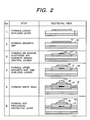
- Fig. 2 shows cross sections at a position on a wafer and where the air bearing surface is supposed to be positioned, for showing fabricating steps.
- the lower shielding layer 10 is formed on a substrate 8 and an insulating layer 9 (step 1).
- the spin valve layer 100, an electrode (70), and the magnetic domain control layer 60 are formed (step 3).
- the upper shielding layer 90 is applied (step 4).
- the write head gap 40 is formed, and after that, the inductive coil, insulating layer, and upper magnetic core 110 are formed (step 5).
- the protective layer 50, terminals, and the like are formed (step 6).
- the wafer step is completed.
- a post step such as an air bearing surface process, cutting, gimbal adhesion, and the like is performed, thereby obtaining the head.
- Fig. 3 shows the sensor part 100 in details, which has the spin valve structure shown in Fig. 1.
- the upper magnetic film is used as a fixed magnetizing direction layer and the lower magnetic film is used as a rotatable magnetizing direction layer.
- the sensor part 100 has a hard bias structure in which a rotatable magnetizing direction layer 53 such as NiFe alloy is formed on a proper under layer 52.
- a non-magnetic interlayer 54, a magnetoresistive change auxiliary layer 55 not necessarily needed, a fixed magnetizing direction layer 56, and an antiferromagnetic layer 66 are sequentially formed.
- An MR sensor layer is limited only in the sensor part, and simultaneously, the magnetic domain control layer 60 and the electrode 70 are formed.
- Fig. 4 shows a bias relation of the spin valve structure. It is necessary to direct the magnetization of the rotatable magnetizing direction layer 53 so as to be perpendicular to the height direction of the MR sensor by a magnetic field obtained by synthesizing a current bias field Hi, a magnetostatic coupling field Hbt from the end of the fixed magnetizing direction layer 56, an interlayer coupling field He and a bias field Hb1 from the magnetic domain control layer 60 by a sense current supplied. Consequently, the magnetizing direction of the fixed magnetizing direction layer has to be in parallel to the height direction of the MR sensor. The recording magnetic field invades the height direction of the MR sensor and vertically turning the magnetization of the rotatable magnetizing direction layer.
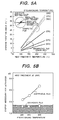
- Fig. 5A shows a method of measuring activation energy of the composite magnetic material used for the shielding layer.
- a pre-annealing (heat treatment) process was performed to a sample by applying a magnetic field in the direction as shown in the diagram, and after that, the magnetizing direction was inclined by 45° and the heat treatment was given.
- the heat treatment was given at temperatures from 100°C to 250°C for three hours, respectively.
- the magnetizing direction after the heat treatment is shown with temperatures.
- the heat treatment was given to the composite film according to the invention shown by dotted lines, in which 4 mol% of SiO2 is added to NiFe. For comparison, results of the CoNbZr amorphous film are also shown by solid lines.
- tan2 ⁇ Ku2/Ku1
- Ku1 magnetic anisotropy remained in the original direction
- Ku2 magnetic anisotropy generated in the 45° direction. It is assumed here that magnetic anisotropy after the pre-annealing process is expressed as Ku0, and Ku1 + Ku2 is equal to Ku0 in the heat treatment at a temperature equal to or lower than the pre-annealing temperature.
- Fig. 5B shows activation energy obtained with respect to the composite film and the amorphous film, respectively, on the basis of the method shown in "Journal of Applied Physics" Vol. 53, p. 2279, 1982.
- the increase in the activation energy is small such as 1.7 to 1.8 eV.
- the pre-annealing temperature is increased from 250°C to 300°C
- the activation energy is increased from 2.2 to 2.7 eV. Since the anisotropy rotation in the composite film is hardly influenced even by the pre-annealing at 300°C, it is found that 1.8 eV or less of the activation energy is sufficient.
- the activation energy of the amorphous film is small just after formation by sputtering, it increases to 2 eV or larger by heating after the head forming process.
- Fig. 6 shows the change in anisotropy of the composite magnetic material by the heat treatment, which is used for the magnetoresistive head according to the invention.
- the magnetization is oriented in the track width direction of the MR sensor as a final magnetizing direction of the shielding layer, the positive magnetic anisotropy is obtained and an anisotropic magnetic field Hk is positive.
- the magnetizing direction perpendicularly crosses the magnetizing direction of the shielding layer (magnetizing direction of the fixed magnetizing direction layer)
- the negative magnetic anisotropy is obtained and the anisotropic magnetic field Hk is turned to be negative.
- a fine line shows the case of the amorphous material.
- Hk 120e just after the formation of the film.
- the magnetic anisotropy was easily turned by the heat treatment at 250°C for 30 minutes and Hk became -60e.
- the heat treatment in the track width direction was given. More than three hours was required so that Hk became smaller than 0.
- Hk was small such as 2 to 30e and the magnetic domain structure was not stabilized.
- the above action is due to the stabilizing phenomenon by the heat treatment to the amorphous material.
- magnetic atoms are easily rearranged and the magnetizing direction can be easily turned.
- it indicates that it is difficult to again turn the magnetizing direction after completion of the process using the long-hour heat treatment. It is important to determine at which stage the magnetic filed is applied in the magnetizing direction of the MR layer during the process. Since the pattern of the shielding layer is large and the shape is isotropic, means for adjusting magnetic deformation and controlling the magnetic anisotropy by using magnetic elastic effect cannot be applied.
- the thick line shows a case of the magnetic head using the composite magnetic film according to the invention, in which 4 to 5 mol% of SiO 2 is added to NiFe.
- Time tcl' required for the turn was 10 minutes.
- Hk was stable after change from +80e to -80e.
- Even the magnetizing direction was again turned after three hours, Hk was recovered to 80e after 10 minutes. That is, it shows that Hk is not stabilized by the heat treatment.
- the NiFe grain growth in the film is inhibitted by oxide and a structure having many grain boundaries is obtained, and that the number of grain boundaries is hardly decreased by the recovery in the heat treatment at 250°C.
- the anisotropy can be returned by the heat treatment even if having any magnetic field history during the process.
- the magnetic domains in the shielding layer are observed by MFM after processing the air bearing surface.
- the percentage of occurrence of the magnetic walls in the lower shielding layer according to the first embodiment is 5% and that in the upper shielding layer is 0%.
- the percentage of occurrence of the magnetic walls in the lower shielding layer is 70% and that in the upper shielding layer is 2%.
- the same shielding layer is used an Al 2 O 3 gap layer of 0.1 ⁇ m is applied as a sensor part, the spin valve part is formed by a fixed magnetizing layer of Ni of 30 nm, NiFe of 0.5 nm, and Co of 5 nm, a rotatable magnetizing direction layer of Cu of 5 nm and NiFe of 10 nm, and Ta of 5 nm, and an Al 2 O 3 gap layer of 0.14 ⁇ m is formed. After a terminal is formed and the heat treatment is given at 200°C for 30 minutes by the magnetic field applied in the height direction of the MR sensor, the heat treatment is given by the magnetic field applied in the track width direction at 150°C for three hours.
- the percentage of occurrence of the magnetic walls in the lower shielding layer is 10% and that in the upper shielding layer is 0%.
- the percentage of occurrence of the magnetic walls in the lower shielding layer is 60% and that in the upper shielding layer is 3%.
- an oxide such as ZrO 2 , TaO 2 , Al 2 O 3 or the like, or a compound such as BN, WC or the like can be also used as the material of the composite magnetic film. It is preferable that an adding amount is 2 to 10 mol% with resect to any case. When the adding amount is too small, the crystal particle size is enlarged and the surface roughness is progressed. When the adding amount exceeds 10 mol%, heat conductivity of the shielding layer deteriorates and a temperature rise in the MR sensor is caused by the current supply.
- the composite magnetic shielding layer is used to both of the upper and lower layers in the head according to the embodiment of the invention, it is also possible that the composite magnetic film is applied only to the lower shielding layer and the amorphous film or a crystalline film such as Ni or Fe is used as the upper shielding layer.
- the method of turning the magnetic anisotropy of the write head after formation is useful especially when a material having a highly saturated magnetic flux density such as CoNiFe in which the magnetic anisotropy is large and the magnetic permeability is small is used.
- Fig. 8 shows a magnetic disk apparatus using the magnetoresistive head according to the invention.
- the apparatus basically comprises: a rotatable magnetic disk 203; a head 204 having magnetoresistive effect for recording and reproducing signals; an actuator 205; and a signal processor.
- the magnetic disk is rotated 4000 to 8000 times per minute by a rotary shaft 202 and the magnetoresistive head 204 is floated above the magnetic disk at an interval of tens to hundreds angstrom.
- an inductive part of the head 204 executes a writing operation, a recording binary digit string is formed concentrically by the rotation of the disk. Further, the head is moved in the radial direction by the actuator 205, thereby recording data on the whole disk.
- a predetermined current is flowed to the magnetoresistive head of the head 204 and the head 204 is moved by the actuator 205 to a predetermined position. After that, a change in resistance of the sensor part is obtained as a change in voltage of the head terminal.
- a reproduction signal is shaped and converted to data by an integrated circuit arranged on a base 201 and is transferred to an external apparatus such as a computer.
- the quality of a reproduction waveform is improved as compared with a case of using the conventional head and a signal read error ratio of the apparatus is improved from 10 -9 to 10 -11 , that is, by more than two digits.
- a signal read error ratio of the apparatus is improved from 10 -9 to 10 -11 , that is, by more than two digits.
- a dual spin valve head having a construction similar to that of Fig. 3 is fabricated by forming a lower fixed magnetizing direction layer 51 and a spacer Ta layer 58 on an NiO layer 59.
- As the lower shielding layer a material in which 4 mol% of SiO 2 is added to NiFe is used.
- the heat treatment to the fixed magnetizing direction layer and the NiMn layer is given in step 3 in Fig. 2.
- the magnetic field is applied in the height direction of the MR sensor after completion of the head and the heat treatment is given at 200°C for 30 minutes. After that, the magnetic field is applied in the track width direction and the heat treatment is given at 160°C for three hours, thereby magnetizing direction of the shielding layer is also oriented in the track width direction.
- an output higher than that of a typical spin valve head by 60% is obtained.
- the recording density is increased by 30% as compared with that of an apparatus using the typical spin valve head.
- a permanent magnetic film such as CoCrPt is used as the magnetic domain control layer.
- the magnetic domain control layer may be omitted. In this case, it is necessary to thin a spacer film and to enhance a coupling magnetic field from the fixed magnetizing direction layer. Although reproduction sensitivity is reduced, reliability of electrical connection at the electrode end is improved.
Landscapes
- Engineering & Computer Science (AREA)
- Chemical & Material Sciences (AREA)
- Nanotechnology (AREA)
- Manufacturing & Machinery (AREA)
- Physics & Mathematics (AREA)
- Crystallography & Structural Chemistry (AREA)
- Electromagnetism (AREA)
- Mathematical Physics (AREA)
- Theoretical Computer Science (AREA)
- Magnetic Heads (AREA)
- Hall/Mr Elements (AREA)
Claims (4)
- Magnetkopf, umfassend:dadurch gekennzeichnet, daß eine Komposit-Magnetschicht, in der einem Material mit drehbarer Magnetisierungsrichtung 2 bis 10 mol% Oxid oder Nitrid beigefügt ist, mindestens in einem Teil der unteren Schicht (10) zur magnetischen Abschirmung verwendet wird.einen magnetoresistiven Kopf, aufweisend: ein Sensorteil (100) mit einer magnetoresistiven Schicht (53) zum Umwandeln eines Magnetsignals in ein elektrisches Signal unter Nutzung des magnetoresistiven Effektes, der durch den relativen Winkel zwischen Magnetisierungsrichtungen von mindestens zwei magnetischen Schichten (53, 56; 51, 53, 56), und einem Elektrodenpaar (70) erzeugt wird, die einen Signalerkennungsstrom an die magnetoresistive Schicht überträgt; untere und obere Schichten (10, 90) zur magnetischen Abschirmung, zwischen denen der Sensorteil angeordnet ist und die die Schicht für den magnetischen Luftspalt bilden; undeinen Schreibkopf, der an der oberen Schicht (90) zur magnetischen Abschirmung des magnetoresistiven Kopfes ausgebildet ist,
- Magnetkopf nach Anspruch 1, wobei eine Komposit-Magnetschicht, in der einem Material mit drehbarer Magnetisierungsrichtung 2 bis 10 mol% Oxid oder Nitrid beigefügt ist, mindestens in einem Teil der oberen Schicht (90) zur magnetischen Abschirmung verwendet wird.
- Magnetkopf nach Anspruch 1 oder 2, wobei die magnetoresistive Schicht eine Schicht (53) mit drehbarer Magnetisierungsrichtung ist, die zwischen zwei Schichten (51, 56) mit fester Magnetisierungsrichtung angeordnet ist.
- Magnetkopf nach Anspruch 1, 2 oder 3, bei dem der magnetoresistive Kopf ferner eine Magnetisierungsbereichs-Steuerschicht (60) umfaßt, um aus der magnetoresistiven Schicht (53) einen einzelnen Magnetisierungsbereich zu bilden.
Applications Claiming Priority (3)
| Application Number | Priority Date | Filing Date | Title |
|---|---|---|---|
| JP12433596A JP3367334B2 (ja) | 1996-05-20 | 1996-05-20 | 磁気ヘッド及びそれを用いた磁気ディスク装置 |
| JP124335/96 | 1996-05-20 | ||
| JP12433596 | 1996-05-20 |
Publications (2)
| Publication Number | Publication Date |
|---|---|
| EP0809237A1 EP0809237A1 (de) | 1997-11-26 |
| EP0809237B1 true EP0809237B1 (de) | 2001-08-16 |
Family
ID=14882804
Family Applications (1)
| Application Number | Title | Priority Date | Filing Date |
|---|---|---|---|
| EP97303307A Expired - Lifetime EP0809237B1 (de) | 1996-05-20 | 1997-05-15 | Magnetkopf und Plattenlaufwerk mit demselben |
Country Status (4)
| Country | Link |
|---|---|
| US (1) | US5969910A (de) |
| EP (1) | EP0809237B1 (de) |
| JP (1) | JP3367334B2 (de) |
| DE (1) | DE69706096T2 (de) |
Families Citing this family (6)
| Publication number | Priority date | Publication date | Assignee | Title |
|---|---|---|---|---|
| US6512661B1 (en) * | 2000-08-10 | 2003-01-28 | Read-Rite Corporation | Vertical giant magnetoresistance sensor utilizing an insulating bias layer |
| US6798623B2 (en) * | 2001-02-08 | 2004-09-28 | Seagate Technology Llc | Biased CPP sensor using spin-momentum transfer |
| US7031122B2 (en) * | 2001-10-26 | 2006-04-18 | Seagate Technology Llc | Magnetic shields for reduced variations of head-media spacing |
| US6775108B2 (en) * | 2001-11-02 | 2004-08-10 | Seagate Technology Llc | Magnetic head having a read element shield and substrate with matching coefficients of thermal expansion |
| US6844144B2 (en) * | 2002-08-27 | 2005-01-18 | Hitachi Global Storage Technologies Netherlands B.V. | Single slider air bearing process using polymer brush formation |
| US7862913B2 (en) * | 2006-10-23 | 2011-01-04 | Hitachi Global Storage Technologies Netherlands B.V. | Oxide magnetic recording layers for perpendicular recording media |
Family Cites Families (4)
| Publication number | Priority date | Publication date | Assignee | Title |
|---|---|---|---|---|
| US4755897A (en) * | 1987-04-28 | 1988-07-05 | International Business Machines Corporation | Magnetoresistive sensor with improved antiferromagnetic film |
| US5446613A (en) * | 1994-02-28 | 1995-08-29 | Read-Rite Corporation | Magnetic head assembly with MR sensor |
| JPH07334819A (ja) * | 1994-06-07 | 1995-12-22 | Alps Electric Co Ltd | 薄膜磁気ヘッド |
| JPH08115511A (ja) * | 1994-10-14 | 1996-05-07 | Hitachi Ltd | フラックスガイド型gmrヘッド |
-
1996
- 1996-05-20 JP JP12433596A patent/JP3367334B2/ja not_active Expired - Fee Related
-
1997
- 1997-05-15 DE DE69706096T patent/DE69706096T2/de not_active Expired - Fee Related
- 1997-05-15 EP EP97303307A patent/EP0809237B1/de not_active Expired - Lifetime
- 1997-05-19 US US08/858,240 patent/US5969910A/en not_active Expired - Lifetime
Also Published As
| Publication number | Publication date |
|---|---|
| DE69706096T2 (de) | 2001-11-22 |
| DE69706096D1 (de) | 2001-09-20 |
| JPH09305927A (ja) | 1997-11-28 |
| US5969910A (en) | 1999-10-19 |
| EP0809237A1 (de) | 1997-11-26 |
| JP3367334B2 (ja) | 2003-01-14 |
Similar Documents
| Publication | Publication Date | Title |
|---|---|---|
| US6023395A (en) | Magnetic tunnel junction magnetoresistive sensor with in-stack biasing | |
| US6282069B1 (en) | Magnetoresistive element having a first antiferromagnetic layer contacting a pinned magnetic layer and a second antiferromagnetic layer contacting a free magnetic layer | |
| KR100223390B1 (ko) | 스핀밸브자기저항소자및그제조방법,스핀밸브자기저항센서,자기기억시스템,자기기록디스크드라이브 | |
| JP4841112B2 (ja) | Mtjセンサ及びディスク・ドライブ・システム | |
| US6005753A (en) | Magnetic tunnel junction magnetoresistive read head with longitudinal and transverse bias | |
| US6870718B2 (en) | Magnetoresistive sensor including magnetic domain control layers having high electric resistivity | |
| JP4128938B2 (ja) | 磁気ヘッド及び磁気記録再生装置 | |
| US6982932B2 (en) | Recording/reproducing head and recording/reproducing apparatus incorporating the same | |
| JPH11134616A (ja) | 磁気抵抗型読取りセンサ、磁気記憶装置及び磁気抵抗型センサの製造方法 | |
| US6175477B1 (en) | Spin valve sensor with nonmagnetic oxide seed layer | |
| US7035061B2 (en) | Magnetoresistive transducer with low magnetic moment, high coercivity stabilizing magnets | |
| US6562487B1 (en) | Writer pole employing a high saturation moment, low permeability layer adjacent to writer gap | |
| US7209326B2 (en) | Magnetoresistive head and manufacturing method thereof | |
| EP0809237B1 (de) | Magnetkopf und Plattenlaufwerk mit demselben | |
| JP2849354B2 (ja) | 磁気変換素子及び薄膜磁気ヘッド | |
| JP2927285B1 (ja) | 磁気抵抗効果型ヘッド | |
| JP2001110008A (ja) | 磁気ヘッドおよびその製造方法、および磁気記録再生装置 | |
| US11683993B2 (en) | Material having both negative spin polarization and negative anisotropy | |
| JP2004128026A (ja) | 磁気抵抗効果素子、磁気ヘッド、磁気記録装置 | |
| JP2821586B2 (ja) | 薄膜磁気ヘッド | |
| WO1997011458A1 (en) | Magnetoresistive head | |
| JPH09251619A (ja) | 磁気抵抗効果型磁気ヘッド及び磁気記録再生装置 | |
| JP2001189505A (ja) | 磁気抵抗効果薄膜の製造方法 | |
| JPH11213345A (ja) | 磁気抵抗効果型磁気ヘッドとその製造方法及び情報記録再生装置 | |
| JPH01105307A (ja) | 薄膜磁気ヘッド・アセンブリ |
Legal Events
| Date | Code | Title | Description |
|---|---|---|---|
| PUAI | Public reference made under article 153(3) epc to a published international application that has entered the european phase |
Free format text: ORIGINAL CODE: 0009012 |
|
| 17P | Request for examination filed |
Effective date: 19970604 |
|
| AK | Designated contracting states |
Kind code of ref document: A1 Designated state(s): DE FR GB |
|
| 17Q | First examination report despatched |
Effective date: 19990416 |
|
| GRAG | Despatch of communication of intention to grant |
Free format text: ORIGINAL CODE: EPIDOS AGRA |
|
| GRAG | Despatch of communication of intention to grant |
Free format text: ORIGINAL CODE: EPIDOS AGRA |
|
| GRAH | Despatch of communication of intention to grant a patent |
Free format text: ORIGINAL CODE: EPIDOS IGRA |
|
| GRAH | Despatch of communication of intention to grant a patent |
Free format text: ORIGINAL CODE: EPIDOS IGRA |
|
| GRAA | (expected) grant |
Free format text: ORIGINAL CODE: 0009210 |
|
| AK | Designated contracting states |
Kind code of ref document: B1 Designated state(s): DE FR GB |
|
| REF | Corresponds to: |
Ref document number: 69706096 Country of ref document: DE Date of ref document: 20010920 |
|
| REG | Reference to a national code |
Ref country code: GB Ref legal event code: IF02 |
|
| ET | Fr: translation filed | ||
| PLBE | No opposition filed within time limit |
Free format text: ORIGINAL CODE: 0009261 |
|
| STAA | Information on the status of an ep patent application or granted ep patent |
Free format text: STATUS: NO OPPOSITION FILED WITHIN TIME LIMIT |
|
| 26N | No opposition filed | ||
| REG | Reference to a national code |
Ref country code: GB Ref legal event code: 732E |
|
| REG | Reference to a national code |
Ref country code: FR Ref legal event code: TP |
|
| PGFP | Annual fee paid to national office [announced via postgrant information from national office to epo] |
Ref country code: GB Payment date: 20080424 Year of fee payment: 12 |
|
| PGFP | Annual fee paid to national office [announced via postgrant information from national office to epo] |
Ref country code: DE Payment date: 20090525 Year of fee payment: 13 |
|
| GBPC | Gb: european patent ceased through non-payment of renewal fee |
Effective date: 20090515 |
|
| REG | Reference to a national code |
Ref country code: FR Ref legal event code: ST Effective date: 20100129 |
|
| PG25 | Lapsed in a contracting state [announced via postgrant information from national office to epo] |
Ref country code: FR Free format text: LAPSE BECAUSE OF NON-PAYMENT OF DUE FEES Effective date: 20090602 |
|
| PGFP | Annual fee paid to national office [announced via postgrant information from national office to epo] |
Ref country code: FR Payment date: 20080423 Year of fee payment: 12 |
|
| PG25 | Lapsed in a contracting state [announced via postgrant information from national office to epo] |
Ref country code: GB Free format text: LAPSE BECAUSE OF NON-PAYMENT OF DUE FEES Effective date: 20090515 |
|
| PG25 | Lapsed in a contracting state [announced via postgrant information from national office to epo] |
Ref country code: DE Free format text: LAPSE BECAUSE OF NON-PAYMENT OF DUE FEES Effective date: 20101201 |