EP0805559B1 - Etage d'attaque - Google Patents
Etage d'attaque Download PDFInfo
- Publication number
- EP0805559B1 EP0805559B1 EP97106966.1A EP97106966A EP0805559B1 EP 0805559 B1 EP0805559 B1 EP 0805559B1 EP 97106966 A EP97106966 A EP 97106966A EP 0805559 B1 EP0805559 B1 EP 0805559B1
- Authority
- EP
- European Patent Office
- Prior art keywords
- field effect
- output
- transistor
- effect transistor
- voltage
- Prior art date
- Legal status (The legal status is an assumption and is not a legal conclusion. Google has not performed a legal analysis and makes no representation as to the accuracy of the status listed.)
- Expired - Lifetime
Links
- 230000001105 regulatory effect Effects 0.000 claims description 3
- 230000005669 field effect Effects 0.000 claims 11
- 239000000758 substrate Substances 0.000 description 2
- 230000001133 acceleration Effects 0.000 description 1
- 239000003990 capacitor Substances 0.000 description 1
- 230000001934 delay Effects 0.000 description 1
- 230000003111 delayed effect Effects 0.000 description 1
- 238000010586 diagram Methods 0.000 description 1
- 230000003993 interaction Effects 0.000 description 1
- 230000007257 malfunction Effects 0.000 description 1
- 238000004519 manufacturing process Methods 0.000 description 1
- 238000005259 measurement Methods 0.000 description 1
- 230000005855 radiation Effects 0.000 description 1
- 239000004065 semiconductor Substances 0.000 description 1
Images

Classifications
-
- H—ELECTRICITY
- H03—ELECTRONIC CIRCUITRY
- H03K—PULSE TECHNIQUE
- H03K19/00—Logic circuits, i.e. having at least two inputs acting on one output; Inverting circuits
- H03K19/003—Modifications for increasing the reliability for protection
- H03K19/00346—Modifications for eliminating interference or parasitic voltages or currents
- H03K19/00361—Modifications for eliminating interference or parasitic voltages or currents in field effect transistor circuits
Definitions
- the invention relates to a driver stage according to the preamble of claim 1.
- Such a driver stage which is designed as a CMOS inverter stage, is eg in Tietze / Schenk semiconductor circuit technology, 8th edition 1986 on page 211ff described.
- Figure 9.36 shows a CMOS inverter.
- the output voltage of such an inverter is either equal to the supply voltage V DD or equal to ground, depending on the input voltage, since one of the two transistors T1 or T2 is always turned on.
- a clock system with non-overlapping clocks is used, in which the size of the Non-overlap time is largely determined by the switching time of the clock driver.
- the switching time of the clock driver or the non-overlap time between the clocks is subject to fluctuations due to operating voltage, temperature and manufacturing influences. Since the non-overlap time to ensure the proper functioning of the digital stages of the microcontroller, a minimum value (1ns), and must not exceed a maximum value, dimensioning in noise-sensitive applications with large clock driver loads is problematic, since with the demand for minimum Non-overlap time at the fastest operating conditions the clock drivers are set.
- Object of the present invention is therefore to provide a driver stage, which does not have the aforementioned disadvantage.
- Advantage of the invention is that are compensated by the use of two separate drive circuits with respective associated voltage regulators for the respective switching transistor of the inverter stage on the one hand influences the supply voltage and on the other mutual influences of the two driver stages are avoided.
- Another advantage results from the use of a pulse generator, which for a particularly fast switching the respective switching transistors is responsible. Disturbances are not avoided but adapted by suitable dimensioning of the pre-driver transistor requirements. A suitable choice of the predriver transistor and main driver transistor advantageously results in a Gaussian shape.
- Another advantage is the particularly low circuit complexity and the reliable operation even at high frequencies.
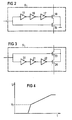
- FIG. 1 1 denotes an input terminal to which the clock signal to be driven is supplied. This input terminal is connected to the gate terminal of a p-channel FET 10 and the gate terminal of an n-channel FET 4.
- the load path of the n-channel FET 4 is connected on the one hand to the load path of the p-channel FET 10 and the gate of a p-channel output FET 2.
- the other load path connection of the p-channel FET 10 is connected to the supply voltage terminal 14.
- the other load path terminal of the n-channel FET 4 is connected to the output of a first voltage regulator 6.
- the voltage regulator 6 further supplies a first pulse generator 8 whose output signal is also supplied to the control terminal of the p-channel output FET 2.
- the pulse generator 8 is controlled by the signal applied to the input terminal 1.
- the input terminal 1 is connected on the one hand to the gate terminal of a p-channel FET 5 and to the gate terminal of an n-channel FET 11.
- the load path of the p-channel FET 5 is connected to the load path of the n-channel FET 11 and to the control terminal of an n-channel output FET 3.
- the other load path terminal of the n-channel FET 11 is connected to ground.
- the other load path terminal of the p-channel FET 5 is connected to the output of a second voltage regulator 7.
- the output signal of the voltage regulator 7 is also supplied to a second pulse generator 9, which in turn is controlled by the voltage applied to the input terminal 1 input signal and whose output signal to the gate terminal of the n-channel output FET 3 is supplied.
- the load path of the p-channel output FET 2 is connected on the one hand to the supply voltage terminal 14 and the other with the load path of the n-channel output FET 3. Its other load path connection is connected to ground. At the junction of the series connection of the load paths of the two output FETs 2, 3, a load is connected to ground, which consists symbolically of the series connection of a resistor 12 and a capacitor 13.
- Transistors 2 and 3 represent the respective driver transistors. In the layout, these large transistors are made up of a plurality of small parallel-connected transistors. In addition to these driver transistors 2, 3 are directly controlled by the input signal shutdown transistors 10 and 11. With these, the respectively not required driver transistor can be turned off quickly and thus an almost complete cross-flow freedom can be achieved. Their implementation in the layout is similar to that in the driver transistors, wherein each parallel-connected driver transistor such a shutdown transistor is assigned.
- the actual pre-driver circuit consists of the pre-driver transistor 4 for the output transistor 2, and the pre-driver transistor 5 for the output transistor 3. With 8 and 9 respectively a pulse generator is referred to, which will be described later.
- FIG. 4 the voltage waveform at the gate of transistor 3 is shown over time generated by this combination of circuits.
- the pulse generator 8 first generates a strong voltage rise up to the voltage V t . Then the pulse ends. At this time, the transistor 4 is also turned on and the voltage at the gate of the output FET 2 continues to increase with a correspondingly shallower rise.
- the output current of the clock signal through the RC load 12, 13 assumes a virtually Gaussian shape.
- Embodiments for the pulse generators 8 and 9 are shown. These are responsible for the acceleration of the switching of the clock drivers with largely the same noise incidence.
- the drive signal is supplied to the one via a series connection of three inverters 15, 16, 17 to the gate terminal of an n-channel FET 18 and the other directly to the gate terminal of another n-channel FET 19th
- the load paths of the two n-channel FETs 18, 19 are connected in series, wherein at one terminal, the output signal is tapped and the other terminal, the output signal of the voltage regulator 6 is supplied.
- the substrate terminals of the FETs 18 and 19 are connected to ground.
- FIG. 3 the input signal from the input terminal 1 to a directly to a gate terminal of a p-channel FET 23 and the other via a series circuit of three inverters 20, 21, 22 the gate terminal of another p-channel FET 24 supplied.
- the load paths of these two FETs 23, 24 are connected in series, wherein the series circuit is acted upon on the one hand with the regulated output voltage of the voltage regulator 7 and on the other hand, the output signal can be tapped.
- the substrate terminals of the two FETs 23 and 24 are also supplied with the regulated output voltage of the voltage regulator 7.
- transistor 19 If a logic "0" signal is present at the input terminal 1, transistor 19 is off and transistor 18 is turned on. If the signal at the input terminal 1 goes from “0" to "1”, then transistor 19 is likewise turned on and the output signal of the voltage regulator 6 is switched to the gate of the output transistor 2 via the load paths of the transistors 18 and 19 conducting at that time.
- the three inverters 15, 16, 17 form a delay chain which delays the input signal at the input terminal 1 to the gate of the transistor 18. After the delay time defined by the three inverter stages 15, 16, 17, the input signal of the input terminal 1 now arrives at the gate of the transistor 18. As a result, it is turned off, whereby the previously mentioned pulse is generated.
- the voltage regulator 6 generates a voltage which always has a constant difference to the supply voltage V DD .
- the delay time can be arbitrarily selected by selecting the number of inverter stages or replaced by an equivalent delay circuit. It is only important that the drive signal to be delayed is inverted.
Landscapes
- Physics & Mathematics (AREA)
- Engineering & Computer Science (AREA)
- Computer Hardware Design (AREA)
- Computing Systems (AREA)
- General Engineering & Computer Science (AREA)
- Mathematical Physics (AREA)
- Electronic Switches (AREA)
- Logic Circuits (AREA)
Claims (3)
- Étage d'attaque comportant deux transistors à effet de champ de sortie (2, 3) de types de conductivité opposés, dont les trajets de charge sont connectés entre la tension d'alimentation et la masse, dans lequel le signal de sortie peut être prélevé au niveau du point de jonction du circuit série des trajets de charge des deux transistors à effet de champ de sortie (2, 3), et dans lequel les bornes de commande des transistors à effet de champ de sortie (2, 3) sont respectivement connectés par l'intermédiaire du trajet de charge d'un transistor à effet de champ supplémentaire (4, 5) du type de conductivité opposé respectif à la sortie d'un régulateur de tension respectif (6, 7), et le signal d'attaque est fourni à la borne de commande du transistor à effet de champ supplémentaire (4, 5),
caractérisé en ce qu'il est prévu un générateur d'impulsions (8, 9) qui est alimenté par le régulateur de tension respectif (6, 7) et est commandé par le signal d'entrée (1) et génère une impulsion de sortie qui est fournie à la grille du transistor à effet de champ de sortie (2, 3), et
en ce que le régulateur de tension (6, 7) génère une tension qui présente toujours une différence constante par rapport à la tension d'alimentation ou à la masse. - Etage d'attaque selon la revendication 1,
caractérisé en ce qu'entre la borne de commande du transistor à effet de champ de sortie (2, 3) et la borne de tension d'alimentation ou la masse, se trouve le trajet de charge d'un transistor de coupure (10, 11) à la borne de commande duquel est appliqué le signal d'entrée (1). - Etage d'attaque selon la revendication 1 ou 2,
caractérisé en ce que le générateur d'impulsions (8, 9) est formé par deux transistors à effet de champ supplémentaires (18, 19 ; 23, 24) qui sont d'un type de conductivité opposé au type de conductivité du transistor à effet de champ de sortie (2 ; 3) et dont les trajets de charge sont connectés en série, dans lequel d'une part, la tension régulée est fournie au trajet de charge du régulateur de tension respectif (6 ; 7) et d'autre part, le signal de sortie peut être prélevé au niveau du trajet de charge, et dans lequel le signal d'entrée (1) est directement appliqué à la borne de commande dudit autre transistor à effet de champ supplémentaire (18, 19 ; 23, 24), et le signal d'entrée (1) est appliqué à la borne de commande de l'autre transistor à effet de champ supplémentaire (18, 19 ; 23, 24) par l'intermédiaire d'un élément à retard inverseur (15, 16, 17 ; 20, 21, 22).
Applications Claiming Priority (2)
| Application Number | Priority Date | Filing Date | Title |
|---|---|---|---|
| DE19617173 | 1996-04-29 | ||
| DE19617173 | 1996-04-29 |
Publications (3)
| Publication Number | Publication Date |
|---|---|
| EP0805559A2 EP0805559A2 (fr) | 1997-11-05 |
| EP0805559A3 EP0805559A3 (fr) | 1998-01-07 |
| EP0805559B1 true EP0805559B1 (fr) | 2013-11-27 |
Family
ID=7792823
Family Applications (1)
| Application Number | Title | Priority Date | Filing Date |
|---|---|---|---|
| EP97106966.1A Expired - Lifetime EP0805559B1 (fr) | 1996-04-29 | 1997-04-25 | Etage d'attaque |
Country Status (1)
| Country | Link |
|---|---|
| EP (1) | EP0805559B1 (fr) |
Family Cites Families (6)
| Publication number | Priority date | Publication date | Assignee | Title |
|---|---|---|---|---|
| US5086238A (en) * | 1985-07-22 | 1992-02-04 | Hitachi, Ltd. | Semiconductor supply incorporating internal power supply for compensating for deviation in operating condition and fabrication process conditions |
| JPH0282713A (ja) * | 1988-09-19 | 1990-03-23 | Fujitsu Ltd | スイッチング補助回路 |
| US5081374A (en) * | 1990-02-22 | 1992-01-14 | National Semiconductor Corporation | Output buffer circuit with signal feed forward for reducing switching induced noise |
| US5128555A (en) * | 1991-03-18 | 1992-07-07 | Motorola, Inc. | Pulsed CMOS logic circuit having selectable rise and fall times |
| US5414312A (en) * | 1993-07-15 | 1995-05-09 | Altera Corporation | Advanced signal driving buffer with directional input transition detection |
| US5440258A (en) * | 1994-02-08 | 1995-08-08 | International Business Machines Corporation | Off-chip driver with voltage regulated predrive |
-
1997
- 1997-04-25 EP EP97106966.1A patent/EP0805559B1/fr not_active Expired - Lifetime
Also Published As
| Publication number | Publication date |
|---|---|
| EP0805559A2 (fr) | 1997-11-05 |
| EP0805559A3 (fr) | 1998-01-07 |
Similar Documents
| Publication | Publication Date | Title |
|---|---|---|
| DE68912277T2 (de) | Ausgangspufferschaltung. | |
| DE112018003130T5 (de) | Zeitsteuerung für Totzeitsteuerung | |
| DE102018126780A1 (de) | Schaltungsanordnung von Gate-Treiber-Schaltungen und Leistungsschaltern mit negativer Sperrspannung | |
| EP0639308B1 (fr) | Circuit pour commander un transistor a effet de champ mos | |
| DE69223715T2 (de) | Integrierte Schaltung mit reduzierten elektromagnetischen Ausstrahlungen | |
| EP1050951B1 (fr) | Arrangement d'un circuit d'alimentation à découpage | |
| DE19725459A1 (de) | Von externer Spannung unabhängiger Sperrvorspannungspegeldetektor | |
| EP0342693A1 (fr) | Système d'alimentation en courant continu avec plusieurs sources de courant continu | |
| DE4324138B4 (de) | CMOS-Drei-Zustands-Pufferschaltung | |
| DE4325899C2 (de) | MOS-Schaltstufe | |
| EP0805559B1 (fr) | Etage d'attaque | |
| DE68916612T2 (de) | ECL/CMOS-Pegelwandler. | |
| DE102007030569B4 (de) | Schaltungsanordnung und Verfahren zum Auswerten eines Datensignals | |
| EP0902541B1 (fr) | Décaleur de niveau de tension | |
| DE4421419C2 (de) | MOS-Treiberschaltung | |
| EP0371163B1 (fr) | Circuit de retard pour signaux impulsionnels, pouvant être intégré | |
| DE102012107024B3 (de) | Schaltung zum strombegrenzten Umladen eines Knotens | |
| EP1439443B9 (fr) | Circuit pour l'alimentation en tension et methode pour produire une tension d' alimentation | |
| DE102004015318B3 (de) | Eingangsschaltung für eine elektronische Schaltung | |
| EP3053270B1 (fr) | Circuit inverseur à limitation de tension | |
| DE4410211B4 (de) | Schaltungsanordnung zur schaltbaren Ansteuerung einer Last | |
| EP1163724A1 (fr) | Circuit de compensation pour circuits d'attaque | |
| EP1438781B1 (fr) | Circuit d'alimentation en tension continue pour des consommateurs raccordes a au moins une ligne | |
| DE19950023A1 (de) | Ansteuervorrichtung für einen Schalter zum elektronischen Schalten eines Verbrauchers | |
| EP3462614A1 (fr) | Structures cascode optimisées |
Legal Events
| Date | Code | Title | Description |
|---|---|---|---|
| PUAI | Public reference made under article 153(3) epc to a published international application that has entered the european phase |
Free format text: ORIGINAL CODE: 0009012 |
|
| AK | Designated contracting states |
Kind code of ref document: A2 Designated state(s): DE FR GB IT |
|
| PUAL | Search report despatched |
Free format text: ORIGINAL CODE: 0009013 |
|
| AK | Designated contracting states |
Kind code of ref document: A3 Designated state(s): DE FR GB IT |
|
| 17P | Request for examination filed |
Effective date: 19980707 |
|
| RAP1 | Party data changed (applicant data changed or rights of an application transferred) |
Owner name: INFINEON TECHNOLOGIES AG |
|
| 17Q | First examination report despatched |
Effective date: 20040722 |
|
| RAP1 | Party data changed (applicant data changed or rights of an application transferred) |
Owner name: INFINEON TECHNOLOGIES AG |
|
| GRAP | Despatch of communication of intention to grant a patent |
Free format text: ORIGINAL CODE: EPIDOSNIGR1 |
|
| INTG | Intention to grant announced |
Effective date: 20130506 |
|
| GRAS | Grant fee paid |
Free format text: ORIGINAL CODE: EPIDOSNIGR3 |
|
| GRAA | (expected) grant |
Free format text: ORIGINAL CODE: 0009210 |
|
| AK | Designated contracting states |
Kind code of ref document: B1 Designated state(s): DE FR GB IT |
|
| REG | Reference to a national code |
Ref country code: GB Ref legal event code: FG4D Free format text: NOT ENGLISH |
|
| REG | Reference to a national code |
Ref country code: DE Ref legal event code: R096 Ref document number: 59713090 Country of ref document: DE Effective date: 20140116 |
|
| REG | Reference to a national code |
Ref country code: DE Ref legal event code: R097 Ref document number: 59713090 Country of ref document: DE |
|
| PLBE | No opposition filed within time limit |
Free format text: ORIGINAL CODE: 0009261 |
|
| STAA | Information on the status of an ep patent application or granted ep patent |
Free format text: STATUS: NO OPPOSITION FILED WITHIN TIME LIMIT |
|
| 26N | No opposition filed |
Effective date: 20140828 |
|
| REG | Reference to a national code |
Ref country code: DE Ref legal event code: R097 Ref document number: 59713090 Country of ref document: DE Effective date: 20140828 |
|
| PG25 | Lapsed in a contracting state [announced via postgrant information from national office to epo] |
Ref country code: IT Free format text: LAPSE BECAUSE OF FAILURE TO SUBMIT A TRANSLATION OF THE DESCRIPTION OR TO PAY THE FEE WITHIN THE PRESCRIBED TIME-LIMIT Effective date: 20131127 |
|
| REG | Reference to a national code |
Ref country code: FR Ref legal event code: PLFP Year of fee payment: 20 |
|
| PGFP | Annual fee paid to national office [announced via postgrant information from national office to epo] |
Ref country code: GB Payment date: 20160421 Year of fee payment: 20 Ref country code: DE Payment date: 20160621 Year of fee payment: 20 |
|
| PGFP | Annual fee paid to national office [announced via postgrant information from national office to epo] |
Ref country code: FR Payment date: 20160421 Year of fee payment: 20 |
|
| REG | Reference to a national code |
Ref country code: DE Ref legal event code: R071 Ref document number: 59713090 Country of ref document: DE |
|
| REG | Reference to a national code |
Ref country code: GB Ref legal event code: PE20 Expiry date: 20170424 |
|
| PG25 | Lapsed in a contracting state [announced via postgrant information from national office to epo] |
Ref country code: GB Free format text: LAPSE BECAUSE OF EXPIRATION OF PROTECTION Effective date: 20170424 |