EP0805559B1 - Driver stage - Google Patents
Driver stage Download PDFInfo
- Publication number
- EP0805559B1 EP0805559B1 EP97106966.1A EP97106966A EP0805559B1 EP 0805559 B1 EP0805559 B1 EP 0805559B1 EP 97106966 A EP97106966 A EP 97106966A EP 0805559 B1 EP0805559 B1 EP 0805559B1
- Authority
- EP
- European Patent Office
- Prior art keywords
- field effect
- output
- transistor
- effect transistor
- voltage
- Prior art date
- Legal status (The legal status is an assumption and is not a legal conclusion. Google has not performed a legal analysis and makes no representation as to the accuracy of the status listed.)
- Expired - Lifetime
Links
- 230000001105 regulatory effect Effects 0.000 claims description 3
- 230000005669 field effect Effects 0.000 claims 11
- 239000000758 substrate Substances 0.000 description 2
- 230000001133 acceleration Effects 0.000 description 1
- 239000003990 capacitor Substances 0.000 description 1
- 230000001934 delay Effects 0.000 description 1
- 230000003111 delayed effect Effects 0.000 description 1
- 238000010586 diagram Methods 0.000 description 1
- 230000003993 interaction Effects 0.000 description 1
- 230000007257 malfunction Effects 0.000 description 1
- 238000004519 manufacturing process Methods 0.000 description 1
- 238000005259 measurement Methods 0.000 description 1
- 230000005855 radiation Effects 0.000 description 1
- 239000004065 semiconductor Substances 0.000 description 1
Images

Classifications
-
- H—ELECTRICITY
- H03—ELECTRONIC CIRCUITRY
- H03K—PULSE TECHNIQUE
- H03K19/00—Logic circuits, i.e. having at least two inputs acting on one output; Inverting circuits
- H03K19/003—Modifications for increasing the reliability for protection
- H03K19/00346—Modifications for eliminating interference or parasitic voltages or currents
- H03K19/00361—Modifications for eliminating interference or parasitic voltages or currents in field effect transistor circuits
Definitions
- the invention relates to a driver stage according to the preamble of claim 1.
- Such a driver stage which is designed as a CMOS inverter stage, is eg in Tietze / Schenk semiconductor circuit technology, 8th edition 1986 on page 211ff described.
- Figure 9.36 shows a CMOS inverter.
- the output voltage of such an inverter is either equal to the supply voltage V DD or equal to ground, depending on the input voltage, since one of the two transistors T1 or T2 is always turned on.
- a clock system with non-overlapping clocks is used, in which the size of the Non-overlap time is largely determined by the switching time of the clock driver.
- the switching time of the clock driver or the non-overlap time between the clocks is subject to fluctuations due to operating voltage, temperature and manufacturing influences. Since the non-overlap time to ensure the proper functioning of the digital stages of the microcontroller, a minimum value (1ns), and must not exceed a maximum value, dimensioning in noise-sensitive applications with large clock driver loads is problematic, since with the demand for minimum Non-overlap time at the fastest operating conditions the clock drivers are set.
- Object of the present invention is therefore to provide a driver stage, which does not have the aforementioned disadvantage.
- Advantage of the invention is that are compensated by the use of two separate drive circuits with respective associated voltage regulators for the respective switching transistor of the inverter stage on the one hand influences the supply voltage and on the other mutual influences of the two driver stages are avoided.
- Another advantage results from the use of a pulse generator, which for a particularly fast switching the respective switching transistors is responsible. Disturbances are not avoided but adapted by suitable dimensioning of the pre-driver transistor requirements. A suitable choice of the predriver transistor and main driver transistor advantageously results in a Gaussian shape.
- Another advantage is the particularly low circuit complexity and the reliable operation even at high frequencies.
- FIG. 1 1 denotes an input terminal to which the clock signal to be driven is supplied. This input terminal is connected to the gate terminal of a p-channel FET 10 and the gate terminal of an n-channel FET 4.
- the load path of the n-channel FET 4 is connected on the one hand to the load path of the p-channel FET 10 and the gate of a p-channel output FET 2.
- the other load path connection of the p-channel FET 10 is connected to the supply voltage terminal 14.
- the other load path terminal of the n-channel FET 4 is connected to the output of a first voltage regulator 6.
- the voltage regulator 6 further supplies a first pulse generator 8 whose output signal is also supplied to the control terminal of the p-channel output FET 2.
- the pulse generator 8 is controlled by the signal applied to the input terminal 1.
- the input terminal 1 is connected on the one hand to the gate terminal of a p-channel FET 5 and to the gate terminal of an n-channel FET 11.
- the load path of the p-channel FET 5 is connected to the load path of the n-channel FET 11 and to the control terminal of an n-channel output FET 3.
- the other load path terminal of the n-channel FET 11 is connected to ground.
- the other load path terminal of the p-channel FET 5 is connected to the output of a second voltage regulator 7.
- the output signal of the voltage regulator 7 is also supplied to a second pulse generator 9, which in turn is controlled by the voltage applied to the input terminal 1 input signal and whose output signal to the gate terminal of the n-channel output FET 3 is supplied.
- the load path of the p-channel output FET 2 is connected on the one hand to the supply voltage terminal 14 and the other with the load path of the n-channel output FET 3. Its other load path connection is connected to ground. At the junction of the series connection of the load paths of the two output FETs 2, 3, a load is connected to ground, which consists symbolically of the series connection of a resistor 12 and a capacitor 13.
- Transistors 2 and 3 represent the respective driver transistors. In the layout, these large transistors are made up of a plurality of small parallel-connected transistors. In addition to these driver transistors 2, 3 are directly controlled by the input signal shutdown transistors 10 and 11. With these, the respectively not required driver transistor can be turned off quickly and thus an almost complete cross-flow freedom can be achieved. Their implementation in the layout is similar to that in the driver transistors, wherein each parallel-connected driver transistor such a shutdown transistor is assigned.
- the actual pre-driver circuit consists of the pre-driver transistor 4 for the output transistor 2, and the pre-driver transistor 5 for the output transistor 3. With 8 and 9 respectively a pulse generator is referred to, which will be described later.
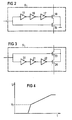
- FIG. 4 the voltage waveform at the gate of transistor 3 is shown over time generated by this combination of circuits.
- the pulse generator 8 first generates a strong voltage rise up to the voltage V t . Then the pulse ends. At this time, the transistor 4 is also turned on and the voltage at the gate of the output FET 2 continues to increase with a correspondingly shallower rise.
- the output current of the clock signal through the RC load 12, 13 assumes a virtually Gaussian shape.
- Embodiments for the pulse generators 8 and 9 are shown. These are responsible for the acceleration of the switching of the clock drivers with largely the same noise incidence.
- the drive signal is supplied to the one via a series connection of three inverters 15, 16, 17 to the gate terminal of an n-channel FET 18 and the other directly to the gate terminal of another n-channel FET 19th
- the load paths of the two n-channel FETs 18, 19 are connected in series, wherein at one terminal, the output signal is tapped and the other terminal, the output signal of the voltage regulator 6 is supplied.
- the substrate terminals of the FETs 18 and 19 are connected to ground.
- FIG. 3 the input signal from the input terminal 1 to a directly to a gate terminal of a p-channel FET 23 and the other via a series circuit of three inverters 20, 21, 22 the gate terminal of another p-channel FET 24 supplied.
- the load paths of these two FETs 23, 24 are connected in series, wherein the series circuit is acted upon on the one hand with the regulated output voltage of the voltage regulator 7 and on the other hand, the output signal can be tapped.
- the substrate terminals of the two FETs 23 and 24 are also supplied with the regulated output voltage of the voltage regulator 7.
- transistor 19 If a logic "0" signal is present at the input terminal 1, transistor 19 is off and transistor 18 is turned on. If the signal at the input terminal 1 goes from “0" to "1”, then transistor 19 is likewise turned on and the output signal of the voltage regulator 6 is switched to the gate of the output transistor 2 via the load paths of the transistors 18 and 19 conducting at that time.
- the three inverters 15, 16, 17 form a delay chain which delays the input signal at the input terminal 1 to the gate of the transistor 18. After the delay time defined by the three inverter stages 15, 16, 17, the input signal of the input terminal 1 now arrives at the gate of the transistor 18. As a result, it is turned off, whereby the previously mentioned pulse is generated.
- the voltage regulator 6 generates a voltage which always has a constant difference to the supply voltage V DD .
- the delay time can be arbitrarily selected by selecting the number of inverter stages or replaced by an equivalent delay circuit. It is only important that the drive signal to be delayed is inverted.
Landscapes
- Physics & Mathematics (AREA)
- Engineering & Computer Science (AREA)
- Computer Hardware Design (AREA)
- Computing Systems (AREA)
- General Engineering & Computer Science (AREA)
- Mathematical Physics (AREA)
- Electronic Switches (AREA)
- Logic Circuits (AREA)
Description
Die Erfindung betrifft eine Treiberstufe gemäß dem Oberbegriff des Anspruchs 1.The invention relates to a driver stage according to the preamble of
Eine derartige Treiberstufe, welche als CMOS-Inverterstufe ausgebildet ist, ist z.B. in
Aufgrund der steigenden Taktfrequenzen und EMV Anforderungen in Mikrocontrolleranwendungen stellen Störungen auf den Versorgungsleitungen, verursacht durch schnelles Schalten großer Ströme, zunehmend ein Problem bei der Schaltungsentwicklung dar.Due to the increasing clock frequencies and EMC requirements in microcontroller applications, disturbances on the supply lines, caused by fast switching of large currents, are increasingly a problem in circuit design.
Im Zusammenwirken der Induktivitäten der Pins und Bonddrähte mit den stets vorhandenen Kapazitäten werden durch schnelles Schalten der Treiberstufen Störschwingungen angeregt, die besonders dann, wenn Analog- und Digitalteile auf einem Chip realisiert werden, zu einer Fehlfunktion führen können. Darüberhinaus kommt es an den Pins zur Abstrahlung elektromagnetischer Wellen, die die Funktion anderer Bauteile beeinträchtigen können.In the interaction of the inductances of the pins and bonding wires with the ever-present capacities are excited by rapid switching of the driver stages spurious vibrations, which can lead to a malfunction especially when analog and digital parts are realized on a chip. In addition, it comes at the pins to the radiation of electromagnetic waves, which may affect the function of other components.
Messungen haben gezeigt, daß die Takttreiber der Mikrocontroller die Hauptquelle, sowohl für die leitungsgeführten, als auch für die abgestrahlten Störungen darstellen.Measurements have shown that the clock drivers of the microcontrollers represent the main source for both the conducted and the radiated disturbances.
Für 8-Bit Mikrocontroller wird z.B. ein Taktsystem mit nichtüberlappenden Takten verwendet, in dem die Größe der Nichtüberlappzeit zum größten Teil von der Schaltzeit des Takttreibers bestimmt wird. Die Schaltzeit der Takttreiber bzw. die Nichtüberlappzeit zwischen den Takten unterliegt Schwankungen aufgrund von Betriebsspannungs-, Temperatur- und Fertigungseinflüssen. Da die Nichtüberlappzeit, um die einwandfreie Funktion der Digitalstufen des Mikrocontrollers zu gewährleisten, einen Minimalwert nicht unterschreiten (1ns), als auch einen Maximalwert nicht überschreiten darf, gestaltet sich die Dimensionierung bei störempfindlichen Anwendungen mit großen Takttreiberlasten als problematisch, da mit der Forderung nach minimaler Nichtüberlappzeit bei den schnellsten Betriebsbedingungen die Takttreiber festgelegt sind. Bei störempfindlichen Anwendungen und großen Takttreiberlasten kann dann die Vergrößerung der Nichtüberlappzeit, der Anstiegs- und Abfallzeit der Takte bei den langsamsten Betriebsbedingungen die Forderung nach einer ausreichender Taktbreite bei einer bestimmten Taktfrequenz unerfüllbar machen. Bei kleineren Takttreiberlasten könnte eine Verringerung der Schwankung der Nichtüberlappzeit den Einsatz des Mikrocontrollers bei höheren Taktfrequenzen ermöglichen.For 8-bit microcontroller, for example, a clock system with non-overlapping clocks is used, in which the size of the Non-overlap time is largely determined by the switching time of the clock driver. The switching time of the clock driver or the non-overlap time between the clocks is subject to fluctuations due to operating voltage, temperature and manufacturing influences. Since the non-overlap time to ensure the proper functioning of the digital stages of the microcontroller, a minimum value (1ns), and must not exceed a maximum value, dimensioning in noise-sensitive applications with large clock driver loads is problematic, since with the demand for minimum Non-overlap time at the fastest operating conditions the clock drivers are set. For noise sensitive applications and large clock driver loads, then, increasing the non-overlap time, the rise and fall times of the clocks at the slowest operating conditions can make the requirement for a sufficient clock width at a particular clock frequency unsatisfiable. For smaller clock driver loads, reducing the non-overlap time variation could allow the use of the microcontroller at higher clock frequencies.
Aufgabe der vorliegenden Erfindung ist es daher eine Treiberstufe anzugeben, welche den vorgenannten Nachteil nicht aufweist.Object of the present invention is therefore to provide a driver stage, which does not have the aforementioned disadvantage.
Diese Aufgabe wird durch den kennzeichnenden Teil des Anspruchs 1 gelöst.This object is solved by the characterizing part of
Vorteil der Erfindung ist es, daß durch die Verwendung von zwei voneinander getrennten Ansteuerschaltungen mit jeweilig zugeordneten Spannungsreglern für den jeweiligen Schalttransistor der Inverterstufe zum einen Einflüsse der Versorgungsspannung ausgeglichen werden und zum anderen gegenseitige Einflüsse der beiden Treiberstufen vermieden werden.Advantage of the invention is that are compensated by the use of two separate drive circuits with respective associated voltage regulators for the respective switching transistor of the inverter stage on the one hand influences the supply voltage and on the other mutual influences of the two driver stages are avoided.
Ein weiterer Vorteil ergibt sich durch die Verwendung eines Pulsgenerators, welcher für ein besonders schnelles Schalten der jeweiligen Schalttransistoren verantwortlich ist. Dabei werden Störungen nicht vermieden sondern durch geeignete Dimensionierung des Vortreibertransistors den Erfordernissen angepaßt. Eine geeignete Wahl des Vortreibertransistors und Haupttreibertransistors ergibt vorteilhafterweise einen gaußförmigen Verlauf.Another advantage results from the use of a pulse generator, which for a particularly fast switching the respective switching transistors is responsible. Disturbances are not avoided but adapted by suitable dimensioning of the pre-driver transistor requirements. A suitable choice of the predriver transistor and main driver transistor advantageously results in a Gaussian shape.
Ein weiterer Vorteil besteht in dem besonders geringen Schaltungsaufwand und der zuverlässigen Arbeitsweise auch bei hohen Frequenzen.Another advantage is the particularly low circuit complexity and the reliable operation even at high frequencies.
Die Erfindung wird nachfolgend anhand von vier Figuren näher erläutert.The invention will be explained in more detail with reference to four figures.
Es zeigen:
Figur 1- ein Prinzipschaltbild der erfindungsgemäßen Anordnung,
Figur 2 und 3- Ausführungsformen der in
Figur 1 Figur 4- einen zeitlichen Verlauf des Ansteuersignals für den Ausgangstransistor.
- FIG. 1
- a schematic diagram of the inventive arrangement,
- FIGS. 2 and 3
- Embodiments of in
FIG. 1 shown pulse generators, - FIG. 4
- a time profile of the drive signal for the output transistor.
In
Des weiteren ist die Eingangsklemme 1 zum einen mit dem Gateanschluß eines p-Kanal-FETS 5 sowie mit dem Gateanschluß eines n-Kanal-FETS 11 verschaltet. Die Laststrecke des p-Kanal-FETS 5 ist mit der Laststrecke des n-Kanal-FETS 11 sowie mit dem Steueranschluß eines n-Kanal-Ausgangs-FETS 3 verbunden. Der andere Laststreckenanschluß des n-Kanal-FETS 11 ist mit Masse verschaltet. Der andere Laststreckenanschluß des p-Kanal-FETS 5 ist mit dem Ausgang eines zweiten Spannungsreglers 7 verbunden. Das Ausgangssignal des Spannungsreglers 7 wird außerdem einem zweiten Pulsgenerator 9 zugeführt, der wiederum durch das an der Eingangsklemme 1 anliegende Eingangssignal gesteuert wird und dessen Ausgangssignal dem Gateanschluß des n-Kanal-Ausgangs-FETS 3 zugeführt wird.Furthermore, the
Die Laststrecke des p-Kanal-Ausgangs-FETS 2 ist zum einen mit der Versorgungsspannungsklemme 14 verschaltet und zum anderen mit der Laststrecke des n-Kanal-Ausgangs-FETS 3. Dessen anderer Laststreckenanschluß ist mit Masse verschaltet. Am Knotenpunkt der Reihenschaltung der Laststrecken der beiden Ausgangs-FETS 2, 3 ist eine Last gegen Masse verschaltet, die symbolisch aus der Reihenschaltung eines Widerstands 12 und einer Kapazität 13 besteht.The load path of the p-
Die Transistoren 2 und 3 stellen die jeweiligen Treibertransistoren dar. Im Layout werden diese großen Transistoren aus mehreren kleinen parallel geschalteten Transistoren aufgebaut. Neben diesen Treibertransistoren 2, 3 befinden sich direkt vom Eingangssignal gesteuerte Abschalttransistoren 10 und 11. Mit diesen kann der jeweils nicht benötigte Treibertransistor schnell ausgeschaltet werden und dadurch eine fast völlige Querstromfreiheit erreicht werden. Ihre Realisierung im Layout erfolgt ähnlich wie bei den Treibertransistoren, wobei jedem parallelgeschalteten Treibertransistor ein derartiger Abschalttransistor zugeordnet wird.
Die eigentliche Funktionsweise wird nachfolgend für einen Ausgangstransistor, nämlich den Ausgangs-FET 2, näher beschrieben. Die Funktionsweise für den spiegelbildlichen Schaltungsteil betreffend den Ausgangs-FET 3 entspricht dieser.The actual mode of operation is described in more detail below for an output transistor, namely the
Die eigentliche Vortreiberschaltung besteht aus dem Vortreibertransistor 4 für den Ausgangstransistor 2, bzw. dem Vortreibertransistor 5 für den Ausgangstransistor 3. Mit 8 bzw. 9 ist jeweils ein Pulsgenerator bezeichnet, der später näher beschrieben wird.The actual pre-driver circuit consists of the
Steigt das Signal an der Eingangsklemme 1 von "0" nach "1", so werden sowohl der Transistor 4 wie auch der Pulsgenerator 8 angesteuert. Beide Elemente werden dabei durch den Spannungsregler 6 versorgt.If the signal at the
In
In
Die Laststrecken der beiden n-Kanal-FETS 18, 19 sind in Reihe geschaltet, wobei an einem Anschluß das Ausgangssignal abgreifbar ist und dem anderen Anschluß das Ausgangssignal des Spannungsreglers 6 zugeführt wird. Die Substratanschlüsse der FETS 18 und 19 sind mit Masse verschaltet.The load paths of the two n-
Ebenso wird in
Liegt an der Eingangsklemme 1 ein logisches "0"-Signal an, so ist Transistor 19 sperrend und Transistor 18 leitend geschaltet. Geht das Signal an der Eingangsklemme 1 von "0" nach "1", so wird Transistor 19 ebenfalls leitend geschaltet und das Ausgangssignal des Spannungsreglers 6 wird über die Laststrecken der zu diesem Zeitpunkt leitenden Transistoren 18 und 19 an das Gate des Ausgangstransistors 2 geschaltet. Die drei Inverter 15, 16, 17 bilden eine Verzögerungskette, welche das Eingangssignal an der Eingangsklemme 1 verzögert auf das Gate des Transistors 18 schalten. Nach der durch die drei Inverterstufen 15, 16, 17 definierten Verzögerungszeit gelangt nun das Eingangssignal der Eingangsklemme 1 an das Gate des Transistors 18. Dadurch wird dieser gesperrt, wodurch der zuvor erwähnte Impuls erzeugt wird.If a logic "0" signal is present at the
Der Spannungsregler 6 erzeugt eine Spannung, welche immer eine konstante Differenz zur Versorgungsspannung VDD aufweist. Der Spannungsregler 7 hingegen erzeugt eine Spannung die immer eine konstante Differenz zu Vss aufweist.The voltage regulator 6 generates a voltage which always has a constant difference to the supply voltage V DD . The voltage regulator 7, however, generates a voltage which always has a constant difference to V ss .
Die Verzögerungszeit kann beliebig durch Wahl der Anzahl von Inverterstufen ausgewählt werden oder durch eine gleichwertige Verzögerungsschaltung ersetzt werden. Wesentlich ist nur, daß das zu verzögernde Ansteuersignal invertiert wird.The delay time can be arbitrarily selected by selecting the number of inverter stages or replaced by an equivalent delay circuit. It is only important that the drive signal to be delayed is inverted.
Claims (3)
- Driver stage having two output field effect transistors (2, 3) of the opposite conduction type, the load paths of which are connected between a supply voltage and earth, the output signal being able to be tapped off at the node of the series circuit of the load paths of the two output field effect transistors (2, 3), and the control connections of the output field effect transistors (2, 3) each being connected to the output of a respective voltage regulator (6, 7) via the load path of a further field effect transistor (4, 5) of the respectively opposite conduction type, and the signal to be driven being supplied to the control connection of the further field effect transistor (4, 5),
characterized
in that a pulse generator (8, 9) is provided, which pulse generator is fed by the respective voltage regulator (6, 7), is controlled by the input signal (1) and generates an output pulse which is supplied to the gate connection of the output field effect transistor (2, 3), and
in that the voltage regulator (6, 7) generates a voltage which always has a constant difference from the supply voltage or from earth. - Driver stage according to Claim 1,
characterized
in that the load path of a disconnection transistor (10, 11) is provided between the control connection of the output field effect transistor (2, 3) and the supply voltage terminal or earth, the input signal (1) being applied to the control connection of said disconnection transistor. - Driver stage according to Claim 1 or 2,
characterized
in that the pulse generator (8, 9) is formed by two further field effect transistors (18, 19; 23, 24) which are of the conduction type opposite to the conduction type of the output field effect transistor (2; 3) and the load paths of which are connected in series, the regulated voltage from the respective voltage regulator (6; 7) being supplied to the load path, on the one hand, and the output signal being able to be tapped off at the load path, on the other hand, and the input signal (1) being directly applied to the control connection of the one further field effect transistor (18, 19; 23, 24), and the input signal (1) being applied to the control connection of the other further field effect transistor (18, 19; 23, 24) via an inverting delay element (15, 16, 17; 20, 21, 22).
Applications Claiming Priority (2)
| Application Number | Priority Date | Filing Date | Title |
|---|---|---|---|
| DE19617173 | 1996-04-29 | ||
| DE19617173 | 1996-04-29 |
Publications (3)
| Publication Number | Publication Date |
|---|---|
| EP0805559A2 EP0805559A2 (en) | 1997-11-05 |
| EP0805559A3 EP0805559A3 (en) | 1998-01-07 |
| EP0805559B1 true EP0805559B1 (en) | 2013-11-27 |
Family
ID=7792823
Family Applications (1)
| Application Number | Title | Priority Date | Filing Date |
|---|---|---|---|
| EP97106966.1A Expired - Lifetime EP0805559B1 (en) | 1996-04-29 | 1997-04-25 | Driver stage |
Country Status (1)
| Country | Link |
|---|---|
| EP (1) | EP0805559B1 (en) |
Family Cites Families (6)
| Publication number | Priority date | Publication date | Assignee | Title |
|---|---|---|---|---|
| US5086238A (en) * | 1985-07-22 | 1992-02-04 | Hitachi, Ltd. | Semiconductor supply incorporating internal power supply for compensating for deviation in operating condition and fabrication process conditions |
| JPH0282713A (en) * | 1988-09-19 | 1990-03-23 | Fujitsu Ltd | Switching auxiliary circuit |
| US5081374A (en) * | 1990-02-22 | 1992-01-14 | National Semiconductor Corporation | Output buffer circuit with signal feed forward for reducing switching induced noise |
| US5128555A (en) * | 1991-03-18 | 1992-07-07 | Motorola, Inc. | Pulsed CMOS logic circuit having selectable rise and fall times |
| US5414312A (en) * | 1993-07-15 | 1995-05-09 | Altera Corporation | Advanced signal driving buffer with directional input transition detection |
| US5440258A (en) * | 1994-02-08 | 1995-08-08 | International Business Machines Corporation | Off-chip driver with voltage regulated predrive |
-
1997
- 1997-04-25 EP EP97106966.1A patent/EP0805559B1/en not_active Expired - Lifetime
Also Published As
| Publication number | Publication date |
|---|---|
| EP0805559A2 (en) | 1997-11-05 |
| EP0805559A3 (en) | 1998-01-07 |
Similar Documents
| Publication | Publication Date | Title |
|---|---|---|
| DE68912277T2 (en) | Output buffer circuit. | |
| DE4423546C2 (en) | Chip initialization signal generation circuit for initializing circuits of a semiconductor memory device | |
| DE112018003130T5 (en) | Time control for dead time control | |
| DE102018126780A1 (en) | Circuit arrangement of gate driver circuits and circuit breakers with negative reverse voltage | |
| EP0639308B1 (en) | Drive circuitry for a mos field effect transistor | |
| DE4322701C1 (en) | Circuit arrangement for a ring oscillator | |
| EP1050951B1 (en) | Circuit arrangement for clocked power supply | |
| DE19725459A1 (en) | Bias voltage level detector | |
| EP0342693A1 (en) | DC power supply system with a plurality of DC sources | |
| DE4324138B4 (en) | CMOS tri-state buffer circuit | |
| EP0805559B1 (en) | Driver stage | |
| DE68916612T2 (en) | ECL / CMOS level converter. | |
| DE102007030569B4 (en) | Circuit arrangement and method for evaluating a data signal | |
| EP0902541B1 (en) | Level Shifter | |
| DE4421419C2 (en) | MOS driver circuit | |
| EP0371163B1 (en) | Delay circuit for pulse signals, suitable for integration | |
| DE102012107024B3 (en) | Current-limited node transferring circuit used in e.g. smart card, has two potential change stages that are dimensioned such that sum of currents flowed between output node and potential supply unit does not exceeds maximum current | |
| DE69500045T2 (en) | Control circuit with zener reference | |
| EP1439443B9 (en) | Circuit for the voltage supply and method for producing a supply voltage | |
| DE102004015318B3 (en) | Input stage for electronic circuit for receiving, evaluating input signal, passing to subsequent stage has control circuit that activates one or other receiving stage depending on current drains of both stages for respective input signal | |
| DE4410211B4 (en) | Circuit arrangement for the switchable control of a load | |
| EP0509075B1 (en) | Circuit for use in motor vehicles for the timed switching of inductive consumers | |
| EP1163724A1 (en) | Compensation circuit for driver circuits | |
| EP0510221A1 (en) | Apparatus for optimizing the operation of MOS driver stages used in synchronous digital circuits | |
| DE19950023A1 (en) | Drive device for switch for electronic switching of loads has semiconducting bridge circuit with clock signal input, charge pump with 42 Volt supply for generating gate voltage for FETs |
Legal Events
| Date | Code | Title | Description |
|---|---|---|---|
| PUAI | Public reference made under article 153(3) epc to a published international application that has entered the european phase |
Free format text: ORIGINAL CODE: 0009012 |
|
| AK | Designated contracting states |
Kind code of ref document: A2 Designated state(s): DE FR GB IT |
|
| PUAL | Search report despatched |
Free format text: ORIGINAL CODE: 0009013 |
|
| AK | Designated contracting states |
Kind code of ref document: A3 Designated state(s): DE FR GB IT |
|
| 17P | Request for examination filed |
Effective date: 19980707 |
|
| RAP1 | Party data changed (applicant data changed or rights of an application transferred) |
Owner name: INFINEON TECHNOLOGIES AG |
|
| 17Q | First examination report despatched |
Effective date: 20040722 |
|
| RAP1 | Party data changed (applicant data changed or rights of an application transferred) |
Owner name: INFINEON TECHNOLOGIES AG |
|
| GRAP | Despatch of communication of intention to grant a patent |
Free format text: ORIGINAL CODE: EPIDOSNIGR1 |
|
| INTG | Intention to grant announced |
Effective date: 20130506 |
|
| GRAS | Grant fee paid |
Free format text: ORIGINAL CODE: EPIDOSNIGR3 |
|
| GRAA | (expected) grant |
Free format text: ORIGINAL CODE: 0009210 |
|
| AK | Designated contracting states |
Kind code of ref document: B1 Designated state(s): DE FR GB IT |
|
| REG | Reference to a national code |
Ref country code: GB Ref legal event code: FG4D Free format text: NOT ENGLISH |
|
| REG | Reference to a national code |
Ref country code: DE Ref legal event code: R096 Ref document number: 59713090 Country of ref document: DE Effective date: 20140116 |
|
| REG | Reference to a national code |
Ref country code: DE Ref legal event code: R097 Ref document number: 59713090 Country of ref document: DE |
|
| PLBE | No opposition filed within time limit |
Free format text: ORIGINAL CODE: 0009261 |
|
| STAA | Information on the status of an ep patent application or granted ep patent |
Free format text: STATUS: NO OPPOSITION FILED WITHIN TIME LIMIT |
|
| 26N | No opposition filed |
Effective date: 20140828 |
|
| REG | Reference to a national code |
Ref country code: DE Ref legal event code: R097 Ref document number: 59713090 Country of ref document: DE Effective date: 20140828 |
|
| PG25 | Lapsed in a contracting state [announced via postgrant information from national office to epo] |
Ref country code: IT Free format text: LAPSE BECAUSE OF FAILURE TO SUBMIT A TRANSLATION OF THE DESCRIPTION OR TO PAY THE FEE WITHIN THE PRESCRIBED TIME-LIMIT Effective date: 20131127 |
|
| REG | Reference to a national code |
Ref country code: FR Ref legal event code: PLFP Year of fee payment: 20 |
|
| PGFP | Annual fee paid to national office [announced via postgrant information from national office to epo] |
Ref country code: GB Payment date: 20160421 Year of fee payment: 20 Ref country code: DE Payment date: 20160621 Year of fee payment: 20 |
|
| PGFP | Annual fee paid to national office [announced via postgrant information from national office to epo] |
Ref country code: FR Payment date: 20160421 Year of fee payment: 20 |
|
| REG | Reference to a national code |
Ref country code: DE Ref legal event code: R071 Ref document number: 59713090 Country of ref document: DE |
|
| REG | Reference to a national code |
Ref country code: GB Ref legal event code: PE20 Expiry date: 20170424 |
|
| PG25 | Lapsed in a contracting state [announced via postgrant information from national office to epo] |
Ref country code: GB Free format text: LAPSE BECAUSE OF EXPIRATION OF PROTECTION Effective date: 20170424 |