EP0804019A2 - Circuit pour la limitation du courant de faisceau d'un tube image - Google Patents
Circuit pour la limitation du courant de faisceau d'un tube image Download PDFInfo
- Publication number
- EP0804019A2 EP0804019A2 EP97106150A EP97106150A EP0804019A2 EP 0804019 A2 EP0804019 A2 EP 0804019A2 EP 97106150 A EP97106150 A EP 97106150A EP 97106150 A EP97106150 A EP 97106150A EP 0804019 A2 EP0804019 A2 EP 0804019A2
- Authority
- EP
- European Patent Office
- Prior art keywords
- beam current
- resistor
- transformer
- circuit
- circuit according
- Prior art date
- Legal status (The legal status is an assumption and is not a legal conclusion. Google has not performed a legal analysis and makes no representation as to the accuracy of the status listed.)
- Granted
Links
Images

Classifications
-
- H—ELECTRICITY
- H04—ELECTRIC COMMUNICATION TECHNIQUE
- H04N—PICTORIAL COMMUNICATION, e.g. TELEVISION
- H04N5/00—Details of television systems
- H04N5/66—Transforming electric information into light information
- H04N5/68—Circuit details for cathode-ray display tubes
-
- H—ELECTRICITY
- H04—ELECTRIC COMMUNICATION TECHNIQUE
- H04N—PICTORIAL COMMUNICATION, e.g. TELEVISION
- H04N3/00—Scanning details of television systems; Combination thereof with generation of supply voltages
- H04N3/10—Scanning details of television systems; Combination thereof with generation of supply voltages by means not exclusively optical-mechanical
- H04N3/16—Scanning details of television systems; Combination thereof with generation of supply voltages by means not exclusively optical-mechanical by deflecting electron beam in cathode-ray tube, e.g. scanning corrections
- H04N3/20—Prevention of damage to cathode-ray tubes in the event of failure of scanning
Definitions
- the invention relates to a circuit for limiting the beam current of a picture tube in a television receiver according to the preamble of claim 1.
- the limiting value is set so that it lies above the beam current with which the picture tube may be subjected to continuous operation without being damaged.
- the long-term average is always below this maximum limitation of the beam current, since there are also dark scenes in which the limitation is not effective. Continuous operation with active beam current limitation is theoretically possible.
- An extreme load case must be taken into account when dimensioning the beam current limiting circuit. This occurs, for example, if the television receiver is operated at an ambient temperature of + 40 ° C for several hours with a completely white picture under extremely poor cooling conditions, such as on a shelf. Even in this extreme load case, the limit values for the high-voltage transformer must not be exceeded.
- the mentioned extreme load case occurs in practice with a device very rarely or never. The need for its consideration in the Dimensioning the beam current limitation, however, limits the scope for the maximum permissible beam current for normal moving images. In other words: If the extreme load case mentioned did not exist with certainty, a higher beam current could be permitted with normal moving images and thus a brighter image could be achieved.
- the invention has for its object to enable a higher beam current for white image areas and thus a brighter image, without the high voltage transformer being endangered in the extreme case mentioned.
- This object is achieved by the invention specified in claim 1.
- Advantageous developments of the invention are specified in the subclaims.
- the invention thus consists in that the transformer contains a temperature sensor, which acts above a certain temperature on the control circuit for the jet current in the sense of a reduction in the jet current.
- the invention is based on the following findings and considerations.
- the extreme load case mentioned cannot be ruled out in practice and must be taken into account when dimensioning the beam current limiting circuit.
- a danger or destruction of the transformer is only possible through an increased temperature of the transformer. Therefore, the temperature of the high-voltage transformer is monitored according to the invention. If the temperature of the transformer and thus also that of the rectifier diodes exceeds a certain value, the beam current is regulated back in the sense of a control loop so that a permissible temperature on the transformer of e.g. 100 °.
- the solution according to the invention has several advantages. There is an imminent danger to the high-voltage transformer in an extreme load case due to the temperature monitoring is recognized and captured, a higher beam current can be permitted for normal operation with moving images and thus a brighter image can be achieved without there being any danger to the transformer.
- the high-voltage transformer remains protected by the temperature control in all cases. In particular, the rectifier diodes cannot reach an inadmissibly high temperature and the core of the transformer cannot reach saturation. If necessary, the high-voltage transformer can be made smaller and cheaper.
- the measure according to the invention requires only a few components, for example a temperature-dependent resistor, an ohmic resistor and a diode.
- the device itself becomes practically indestructible, even if, in extreme cases, it is operated at + 40 ° C ambient temperature under poor cooling conditions for a number of hours with a completely white picture.
- the brightness is reduced in the extreme case mentioned.
- this is practically not a disadvantage, since in the extreme case of stress mentioned there is no normal picture anyway, the change in brightness is noticeably slow with suitable dimensioning and this case usually only rarely or never occurs with a particular device.
- the circuit controlled by the temperature sensor is preferably dimensioned such that it does not respond to long-term beam current behavior due to moving images with normal average brightness.
- the temperature sensor is preferably formed by a temperature-dependent resistor, a so-called NTC or PTC resistor. Such resistors are commercially available and inexpensive.
- the temperature sensor in the form of a temperature-dependent resistor is preferably cast into a plastic body together with the coil former, the windings and the rectifier diodes. The ends of the resistor are connected to two terminals of the transformer. It has been shown that with this solution, the temperature of the resistor with sufficient accuracy and time constant of the temperature of the Rectifier diodes follow. The temperature at the temperature-dependent resistor is therefore a real measure of the temperature of the rectifier diodes.
- the temperature-dependent resistance is close to the core of the transformer. This also ensures that the temperature of the resistor follows the temperature of the rectifier diodes with sufficient accuracy and speed.
- This arrangement has the advantage that the core is at ground potential, ie not in the high-voltage range, and thus there are no insulation problems with the temperature-dependent resistor.
- the resistance can also be between the core and a printed circuit board carrying the transformer.
- the arrangement is such that the heat from the core is transferred as well as possible to the resistor, but as little as possible to the printed circuit board and the conductor tracks contained on it.
- the temperature dependent resistance can also be in a recess such as a notch on a surface of the core.
- the thermal contact between the core and the resistor can be improved further by the core being in direct contact with the resistor at approximately 180 ° the circumference thereof.
- the temperature-dependent resistor can also be embedded in a plastic body which is enclosed between the core and the printed circuit board.
- the temperature sensor preferably forms part of a network which is connected via a threshold circuit to a control terminal of a picture tube control circuit which influences the beam current.
- the series connection of the temperature-dependent resistor and a further ohmic resistor is between an operating voltage and earth, and the center point of the series connection is over a Diode connected to the control terminal influencing the beam current.
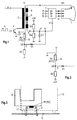
- Fig. 1 shows the high voltage transformer Tr, which supplies the high voltage UH for the picture tube 1 of a television receiver.
- the primary winding 2 of the transformer Tr is connected to the operating voltage + UB and to ground via a switching transistor 4 actuated periodically by the switching voltage 3.
- the high-voltage winding 5 is designed as a diode split winding with a plurality of high-voltage rectifier diodes 6.
- the control signals R, G, B are fed to the picture tube 1 via the video output amplifier 7 and control the beam currents is in the picture tube 1.
- a circuit for limiting the beam current is provided with the resistors R3 and R4 and the capacitor C1.
- the resistors R3 and R4 form a voltage divider with the filter capacitor C1.
- the resistor R3 is connected to the operating voltage + U2 and acts as a current source. If the beam current flowing through resistor R4 is zero, only a current of + U2 flows through resistor R3 into resistor R4 and generates a voltage U4 at point b.
- the high-voltage winding 5 takes over part of the current through the resistor R3 and thereby reduces the voltage across the resistor R3 to lower or even negative values.
- the voltage U4 is the correcting variable for the Beam current limitation applied to the control terminal a of the video amplifier 7. The circuit described so far is known.
- the resistor R2 lies closely on the ferrite core 8 of the transformer Tr.
- the voltage divider consisting of the resistors R1, R2 thus supplies a voltage which is dependent on the respective temperature of the ferrite core 8.
- the voltage U3 is greater than the voltage U4, so that the point c is decoupled from the point b by the blocked diode D1.
- R2 becomes less resistive, so that the voltage U3 drops.
- the voltage U3 finally becomes lower than the voltage U4 and thus the diode D1 conducts. Then a part of the current coming from the resistor R3 flows through the conductive diode D1 and no longer through the high-voltage winding 5. This means that the threshold value of the beam current limiter slowly decreases and thus the transmitted power is reduced as desired. This is a closed loop, the losses in the ferrite core 8 being reduced together with the transmitted power and the temperature being regulated and stabilized to an absolute value which is no longer dangerous for the transformer.
- the voltage divider consisting of the resistors R1 and R2 determines the point at which the beam current limitation controlled by the temperature of the transformer Tr becomes active.
- FIG. 2 shows a modification of the circuit according to FIG. 1.
- the resistor R1 is designed as an NTC resistor and is arranged on the ferrite core 8.
- the mode of operation is practically the same as in FIG. 1.
- the resistance R1 becomes more high-resistance, so that, as in FIG. 1, the voltage U3 at point c decreases and finally the diode D1 becomes conductive above a certain temperature and triggers the beam current limitation.
- FIG. 3 shows the arrangement of the resistor R1 according to FIG. 2 or R1 according to FIG. 2 on the ferrite core 8.
- the resistor R1 or R2 is embedded in a plastic body 9 which lies between the lower edge of the ferrite core 8 and the printed circuit board 10 and is held by the bracket 11.
- the housing of the high-voltage transformer Tr is symbolically indicated by the plastic body 12.
- the temperature-dependent resistor R1 or R2 is also cast into the plastic body 12, into which the coil former, the primary winding 2 arranged thereon, the secondary winding 6 and, if appropriate, additional windings and the high-voltage rectifier diodes are also cast.
- the ends of the resistor R1 or R2 are connected with two additional connection pins 20 which engage in corresponding conductor tracks on the printed circuit board 10 and effect the switching of the resistor R1 or R2 according to FIG. 1 or 2.
- the plastic body 12, which represents the actual housing of the transformer, furthermore contains a large number of connection pins 21 for the primary winding, the high-voltage winding and, if appropriate, further additional windings.
- connection pins 21 are also connected to corresponding conductor tracks on the underside of the printed circuit board 10. This arrangement of the resistor R1 or R2 in the casting compound of the plastic body 12 without immediate contact with the core 8 also ensures that the resistor R1 or R2 follows the temperature of the high-voltage rectifier diodes cast into the plastic body 12 with sufficient accuracy and time constant.
- FIG. 5 shows a simplified block diagram of the picture tube control circuit of the television receiver, which contains the solution according to the invention according to FIGS. 1 to 4.
- the high voltage stage 13, which includes the transformer Tr, delivers the High voltage UH for the picture tube 1, the information IT about the temperature of the ferrite core 8 and the information Iis about the respective value of the beam current is to the interface circuit 14.
- the circuit 14 supplies the manipulated variable Bis for the beam current limitation to the video processor 7, the supplies the control signals R, G, B to the picture tube 1.
- the signals R, G, B are fed to the video processor 7 from a known signal processing circuit.
- the microprocessor 15 supplies control signals for the contrast K and the brightness H to the processor 7.
- the line 16 shown in dotted lines can optionally also be used, since the control loop can be closed via the microprocessor 15. This is also able to control the beam current by adjusting the contrast and brightness, as is generally done within the video processor 7.
Landscapes
- Engineering & Computer Science (AREA)
- Multimedia (AREA)
- Signal Processing (AREA)
- Details Of Television Scanning (AREA)
- Transforming Electric Information Into Light Information (AREA)
- Processing Of Color Television Signals (AREA)
Applications Claiming Priority (2)
| Application Number | Priority Date | Filing Date | Title |
|---|---|---|---|
| DE19616272 | 1996-04-24 | ||
| DE19616272A DE19616272A1 (de) | 1996-04-24 | 1996-04-24 | Schaltung zur Begrenzung des Strahlstroms einer Bildröhre |
Publications (3)
| Publication Number | Publication Date |
|---|---|
| EP0804019A2 true EP0804019A2 (fr) | 1997-10-29 |
| EP0804019A3 EP0804019A3 (fr) | 1997-11-19 |
| EP0804019B1 EP0804019B1 (fr) | 2002-07-24 |
Family
ID=7792246
Family Applications (1)
| Application Number | Title | Priority Date | Filing Date |
|---|---|---|---|
| EP97106150A Expired - Lifetime EP0804019B1 (fr) | 1996-04-24 | 1997-04-15 | Circuit pour la limitation du courant de faisceau d'un tube image |
Country Status (5)
| Country | Link |
|---|---|
| US (1) | US6040664A (fr) |
| EP (1) | EP0804019B1 (fr) |
| JP (1) | JPH1070693A (fr) |
| CN (1) | CN1160951C (fr) |
| DE (2) | DE19616272A1 (fr) |
Families Citing this family (4)
| Publication number | Priority date | Publication date | Assignee | Title |
|---|---|---|---|---|
| JP3833843B2 (ja) * | 1999-04-06 | 2006-10-18 | Necディスプレイソリューションズ株式会社 | 画像補正方法及び画像補正装置並びに陰極線管ディスプレイ装置 |
| US6636265B1 (en) * | 2000-01-21 | 2003-10-21 | Thomson Licensing S.A. | Focus flutter prevention in TV receivers and monitors |
| KR20040068680A (ko) * | 2003-01-27 | 2004-08-02 | 삼성전자주식회사 | 고압 변압기 |
| KR20080079449A (ko) | 2007-02-27 | 2008-09-01 | 삼성전자주식회사 | 영상 디스플레이장치 및 영상 디스플레이장치에서의 과전류제어방법 |
Family Cites Families (6)
| Publication number | Priority date | Publication date | Assignee | Title |
|---|---|---|---|---|
| JPS5630985B2 (fr) * | 1973-10-16 | 1981-07-18 | ||
| US4042858A (en) * | 1976-07-08 | 1977-08-16 | Gte Sylvania Incorporated | Television receiver protection circuit |
| US4126816A (en) * | 1977-05-13 | 1978-11-21 | Rca Corporation | High voltage protection circuit |
| US4645988A (en) * | 1985-12-11 | 1987-02-24 | Zenith Electronics Corporation | Temperature compensated drive circuit for CRT G2 grid |
| US4945414A (en) * | 1988-05-12 | 1990-07-31 | Rca Licensing Corporation | Compensator for temperature-induced black level drift for use in a television receiver |
| JPH04134973A (ja) * | 1990-09-26 | 1992-05-08 | Mitsubishi Electric Corp | フライバックトランスの発煙防止装置 |
-
1996
- 1996-04-24 DE DE19616272A patent/DE19616272A1/de not_active Withdrawn
-
1997
- 1997-03-24 CN CNB971030855A patent/CN1160951C/zh not_active Expired - Fee Related
- 1997-04-15 DE DE59707761T patent/DE59707761D1/de not_active Expired - Fee Related
- 1997-04-15 EP EP97106150A patent/EP0804019B1/fr not_active Expired - Lifetime
- 1997-04-22 JP JP9103740A patent/JPH1070693A/ja active Pending
-
1998
- 1998-02-25 US US08/999,879 patent/US6040664A/en not_active Expired - Fee Related
Also Published As
| Publication number | Publication date |
|---|---|
| CN1171695A (zh) | 1998-01-28 |
| CN1160951C (zh) | 2004-08-04 |
| EP0804019A3 (fr) | 1997-11-19 |
| DE59707761D1 (de) | 2002-08-29 |
| JPH1070693A (ja) | 1998-03-10 |
| EP0804019B1 (fr) | 2002-07-24 |
| US6040664A (en) | 2000-03-21 |
| DE19616272A1 (de) | 1997-10-30 |
Similar Documents
| Publication | Publication Date | Title |
|---|---|---|
| DE2834678C2 (de) | Schaltungsanordnung mit Kurzschlußschutz | |
| EP0804019B1 (fr) | Circuit pour la limitation du courant de faisceau d'un tube image | |
| DE69838973T2 (de) | Schwachstromüberwachung durch "low-side" getriebenen DMOS mittels Modulierung seines inneren Widerstands | |
| DE2700274A1 (de) | Stromversorgungseinrichtung fuer bildverstaerker | |
| DE3510798C2 (fr) | ||
| DE1137795B (de) | Elektrisches Schutzrelais | |
| DE3723579C1 (de) | Laengsspannungsregler | |
| DE3000595C2 (fr) | ||
| DE2930216C2 (fr) | ||
| EP0018598A1 (fr) | Circuit pour limiter le courant de commutation dans un circuit série comprenant un transformateur de courant, un élément semi-conducteur de commutation, une inductance de protection et un circuit de déclenchement par surintensité de courant | |
| DE3891380C2 (de) | Verstärker mit vier Transistoren, die in einer Brückenschaltung miteinander verbunden sind | |
| DE2115379C3 (de) | Ablenkstufe für einen Fernsehempfänger | |
| DE1168962B (de) | Schaltungsanordnung zur Vermeidung einer UEberlastung eines Schalttransistors | |
| DE2736966A1 (de) | Sender fuer optische strahlung | |
| DE3726244C2 (de) | Schaltungsanordnung zur Überwachung der Leistung einer Laserdiode | |
| DE2733006B2 (de) | Temperaturwächter | |
| DE3032970C2 (de) | Schaltungsanordnung zur Symmetrierung der Arbeitspunkte bei elektronisch gleichstromgespeisten Anschlußleitungen in Fernmelde-, insbesondere Fernsprechvermittlungsanlagen | |
| DE3878945T2 (de) | Vorrichtung zur speisung elektrischer energie fuer ein kabel und seine anwendung. | |
| EP3794701B1 (fr) | Circuit de protection d'un composant électronique | |
| DE1093407B (de) | Schaltungsanordnung mit einer Bildaufnahmeroehre vom Vidikontyp | |
| DE3314299C1 (de) | Schaltungsanordnung zur Einstellung des Schwarzpegels von Videosignalen | |
| DE19709681A1 (de) | Schaltung zur Überwachung des Strahlstroms in einer Farbildröhre | |
| DE1563633C3 (de) | Stromversorgungsschaltung | |
| DE19833968A1 (de) | Integrierte Reglervorrichtung | |
| DE2906010B2 (de) | Schaltung zur Verarbeitung von Videosignalen mit einer Überlastschutzschaltung |
Legal Events
| Date | Code | Title | Description |
|---|---|---|---|
| PUAI | Public reference made under article 153(3) epc to a published international application that has entered the european phase |
Free format text: ORIGINAL CODE: 0009012 |
|
| PUAL | Search report despatched |
Free format text: ORIGINAL CODE: 0009013 |
|
| AK | Designated contracting states |
Kind code of ref document: A2 Designated state(s): DE FR GB IT |
|
| AK | Designated contracting states |
Kind code of ref document: A3 Designated state(s): DE FR GB IT |
|
| 17P | Request for examination filed |
Effective date: 19980505 |
|
| 17Q | First examination report despatched |
Effective date: 20000120 |
|
| GRAG | Despatch of communication of intention to grant |
Free format text: ORIGINAL CODE: EPIDOS AGRA |
|
| GRAG | Despatch of communication of intention to grant |
Free format text: ORIGINAL CODE: EPIDOS AGRA |
|
| GRAH | Despatch of communication of intention to grant a patent |
Free format text: ORIGINAL CODE: EPIDOS IGRA |
|
| GRAH | Despatch of communication of intention to grant a patent |
Free format text: ORIGINAL CODE: EPIDOS IGRA |
|
| GRAA | (expected) grant |
Free format text: ORIGINAL CODE: 0009210 |
|
| AK | Designated contracting states |
Kind code of ref document: B1 Designated state(s): DE FR GB IT |
|
| REG | Reference to a national code |
Ref country code: GB Ref legal event code: FG4D Free format text: NOT ENGLISH |
|
| GBT | Gb: translation of ep patent filed (gb section 77(6)(a)/1977) |
Effective date: 20020725 |
|
| REG | Reference to a national code |
Ref country code: GB Ref legal event code: 746 Effective date: 20020807 |
|
| REF | Corresponds to: |
Ref document number: 59707761 Country of ref document: DE Date of ref document: 20020829 |
|
| ET | Fr: translation filed | ||
| REG | Reference to a national code |
Ref country code: FR Ref legal event code: D6 |
|
| PLBE | No opposition filed within time limit |
Free format text: ORIGINAL CODE: 0009261 |
|
| STAA | Information on the status of an ep patent application or granted ep patent |
Free format text: STATUS: NO OPPOSITION FILED WITHIN TIME LIMIT |
|
| 26N | No opposition filed |
Effective date: 20030425 |
|
| PGFP | Annual fee paid to national office [announced via postgrant information from national office to epo] |
Ref country code: GB Payment date: 20080326 Year of fee payment: 12 |
|
| PGFP | Annual fee paid to national office [announced via postgrant information from national office to epo] |
Ref country code: IT Payment date: 20090427 Year of fee payment: 13 Ref country code: DE Payment date: 20090423 Year of fee payment: 13 |
|
| GBPC | Gb: european patent ceased through non-payment of renewal fee |
Effective date: 20090415 |
|
| REG | Reference to a national code |
Ref country code: FR Ref legal event code: ST Effective date: 20091231 |
|
| PG25 | Lapsed in a contracting state [announced via postgrant information from national office to epo] |
Ref country code: GB Free format text: LAPSE BECAUSE OF NON-PAYMENT OF DUE FEES Effective date: 20090415 Ref country code: FR Free format text: LAPSE BECAUSE OF NON-PAYMENT OF DUE FEES Effective date: 20091222 |
|
| PGFP | Annual fee paid to national office [announced via postgrant information from national office to epo] |
Ref country code: FR Payment date: 20080425 Year of fee payment: 12 |
|
| PG25 | Lapsed in a contracting state [announced via postgrant information from national office to epo] |
Ref country code: DE Free format text: LAPSE BECAUSE OF NON-PAYMENT OF DUE FEES Effective date: 20101103 |
|
| PG25 | Lapsed in a contracting state [announced via postgrant information from national office to epo] |
Ref country code: IT Free format text: LAPSE BECAUSE OF NON-PAYMENT OF DUE FEES Effective date: 20100415 |