EP0803907A2 - Ribbon, bonding wire and microwave circuit package - Google Patents
Ribbon, bonding wire and microwave circuit package Download PDFInfo
- Publication number
- EP0803907A2 EP0803907A2 EP97105797A EP97105797A EP0803907A2 EP 0803907 A2 EP0803907 A2 EP 0803907A2 EP 97105797 A EP97105797 A EP 97105797A EP 97105797 A EP97105797 A EP 97105797A EP 0803907 A2 EP0803907 A2 EP 0803907A2
- Authority
- EP
- European Patent Office
- Prior art keywords
- ribbon
- microwave circuit
- width
- circuit package
- bonding
- Prior art date
- Legal status (The legal status is an assumption and is not a legal conclusion. Google has not performed a legal analysis and makes no representation as to the accuracy of the status listed.)
- Granted
Links
Images



Classifications
-
- H—ELECTRICITY
- H10—SEMICONDUCTOR DEVICES; ELECTRIC SOLID-STATE DEVICES NOT OTHERWISE PROVIDED FOR
- H10W—GENERIC PACKAGES, INTERCONNECTIONS, CONNECTORS OR OTHER CONSTRUCTIONAL DETAILS OF DEVICES COVERED BY CLASS H10
- H10W72/00—Interconnections or connectors in packages
- H10W72/851—Dispositions of multiple connectors or interconnections
-
- H—ELECTRICITY
- H10—SEMICONDUCTOR DEVICES; ELECTRIC SOLID-STATE DEVICES NOT OTHERWISE PROVIDED FOR
- H10W—GENERIC PACKAGES, INTERCONNECTIONS, CONNECTORS OR OTHER CONSTRUCTIONAL DETAILS OF DEVICES COVERED BY CLASS H10
- H10W44/00—Electrical arrangements for controlling or matching impedance
- H10W44/20—Electrical arrangements for controlling or matching impedance at high-frequency [HF] or radio frequency [RF]
-
- H—ELECTRICITY
- H10—SEMICONDUCTOR DEVICES; ELECTRIC SOLID-STATE DEVICES NOT OTHERWISE PROVIDED FOR
- H10W—GENERIC PACKAGES, INTERCONNECTIONS, CONNECTORS OR OTHER CONSTRUCTIONAL DETAILS OF DEVICES COVERED BY CLASS H10
- H10W99/00—Subject matter not provided for in other groups of this subclass
-
- H—ELECTRICITY
- H10—SEMICONDUCTOR DEVICES; ELECTRIC SOLID-STATE DEVICES NOT OTHERWISE PROVIDED FOR
- H10W—GENERIC PACKAGES, INTERCONNECTIONS, CONNECTORS OR OTHER CONSTRUCTIONAL DETAILS OF DEVICES COVERED BY CLASS H10
- H10W44/00—Electrical arrangements for controlling or matching impedance
- H10W44/20—Electrical arrangements for controlling or matching impedance at high-frequency [HF] or radio frequency [RF]
- H10W44/203—Electrical connections
- H10W44/206—Wires
-
- H—ELECTRICITY
- H10—SEMICONDUCTOR DEVICES; ELECTRIC SOLID-STATE DEVICES NOT OTHERWISE PROVIDED FOR
- H10W—GENERIC PACKAGES, INTERCONNECTIONS, CONNECTORS OR OTHER CONSTRUCTIONAL DETAILS OF DEVICES COVERED BY CLASS H10
- H10W72/00—Interconnections or connectors in packages
- H10W72/071—Connecting or disconnecting
- H10W72/075—Connecting or disconnecting of bond wires
- H10W72/07531—Techniques
- H10W72/07532—Compression bonding, e.g. thermocompression bonding
-
- H—ELECTRICITY
- H10—SEMICONDUCTOR DEVICES; ELECTRIC SOLID-STATE DEVICES NOT OTHERWISE PROVIDED FOR
- H10W—GENERIC PACKAGES, INTERCONNECTIONS, CONNECTORS OR OTHER CONSTRUCTIONAL DETAILS OF DEVICES COVERED BY CLASS H10
- H10W72/00—Interconnections or connectors in packages
- H10W72/071—Connecting or disconnecting
- H10W72/075—Connecting or disconnecting of bond wires
- H10W72/07531—Techniques
- H10W72/07532—Compression bonding, e.g. thermocompression bonding
- H10W72/07533—Ultrasonic bonding, e.g. thermosonic bonding
-
- H—ELECTRICITY
- H10—SEMICONDUCTOR DEVICES; ELECTRIC SOLID-STATE DEVICES NOT OTHERWISE PROVIDED FOR
- H10W—GENERIC PACKAGES, INTERCONNECTIONS, CONNECTORS OR OTHER CONSTRUCTIONAL DETAILS OF DEVICES COVERED BY CLASS H10
- H10W72/00—Interconnections or connectors in packages
- H10W72/50—Bond wires
- H10W72/531—Shapes of wire connectors
- H10W72/533—Cross-sectional shape
-
- H—ELECTRICITY
- H10—SEMICONDUCTOR DEVICES; ELECTRIC SOLID-STATE DEVICES NOT OTHERWISE PROVIDED FOR
- H10W—GENERIC PACKAGES, INTERCONNECTIONS, CONNECTORS OR OTHER CONSTRUCTIONAL DETAILS OF DEVICES COVERED BY CLASS H10
- H10W72/00—Interconnections or connectors in packages
- H10W72/50—Bond wires
- H10W72/531—Shapes of wire connectors
- H10W72/533—Cross-sectional shape
- H10W72/534—Cross-sectional shape being rectangular
-
- H—ELECTRICITY
- H10—SEMICONDUCTOR DEVICES; ELECTRIC SOLID-STATE DEVICES NOT OTHERWISE PROVIDED FOR
- H10W—GENERIC PACKAGES, INTERCONNECTIONS, CONNECTORS OR OTHER CONSTRUCTIONAL DETAILS OF DEVICES COVERED BY CLASS H10
- H10W72/00—Interconnections or connectors in packages
- H10W72/50—Bond wires
- H10W72/531—Shapes of wire connectors
- H10W72/536—Shapes of wire connectors the connected ends being ball-shaped
-
- H—ELECTRICITY
- H10—SEMICONDUCTOR DEVICES; ELECTRIC SOLID-STATE DEVICES NOT OTHERWISE PROVIDED FOR
- H10W—GENERIC PACKAGES, INTERCONNECTIONS, CONNECTORS OR OTHER CONSTRUCTIONAL DETAILS OF DEVICES COVERED BY CLASS H10
- H10W72/00—Interconnections or connectors in packages
- H10W72/50—Bond wires
- H10W72/541—Dispositions of bond wires
- H10W72/5445—Dispositions of bond wires being orthogonal to a side surface of the chip, e.g. parallel arrangements
-
- H—ELECTRICITY
- H10—SEMICONDUCTOR DEVICES; ELECTRIC SOLID-STATE DEVICES NOT OTHERWISE PROVIDED FOR
- H10W—GENERIC PACKAGES, INTERCONNECTIONS, CONNECTORS OR OTHER CONSTRUCTIONAL DETAILS OF DEVICES COVERED BY CLASS H10
- H10W90/00—Package configurations
- H10W90/701—Package configurations characterised by the relative positions of pads or connectors relative to package parts
- H10W90/751—Package configurations characterised by the relative positions of pads or connectors relative to package parts of bond wires
- H10W90/754—Package configurations characterised by the relative positions of pads or connectors relative to package parts of bond wires between a chip and a stacked insulating package substrate, interposer or RDL
Definitions
- the present invention relates to an improvement in a microwave circuit package for sealing therein microwave circuitry having monolithic microwave integrated circuits (hereinafter referred to as MMICs), as well as to ribbons and bonding wires for use in fabricating the microwave circuit package.
- MMICs monolithic microwave integrated circuits
- bonding wires having uniform diameters along their lengths, ribbons of uniform thickness and/or mesh ribbons, have been used for mounting high-frequency devices to a metallic substrate in a microwave circuit package.
- Japanese Patent Laid-Open Publication No. HEI 1-300546 discloses a microwave circuit package in which electrostatic capacity is provided externally of an area of an MMIC chip by forming a dielectric layer between a metallic substrate and a biasing direct current (DC) terminal.
- DC direct current
- a microwave circuit package be fabricated using metallic substrates, MMICs and bonding wires which are altered in their materials, while rendering the microwave circuit package to be compatible with a separate microwave circuit package fabricated using the same components but not involving such changes in material, by varying the post-mounting high-frequency characteristics of the MMIC and so forth.
- the post-mounting high-frequency characteristics of the MMICs may be varied by changing the lengths of the ribbons and bonding wires.
- connection through the bonding wires requires of the latter to be gently curved in a proper manner.
- length alteration of the bonding wires is limited due to the limited space within the microwave circuit package.
- Another possible approach would be to change the spacing between the components such as the MMICs to allow alteration of the lengths of the ribbons.
- the space alteration is also limited and hence is not an effective solution.
- Another object of the present invention is to provide a microwave circuit package having a metallic substrate and sealing therein an MMIC mounted to the metallic substrate, the microwave circuit package further comprising a circuit or circuit element having a ribbon and/or a bonding wire assembled thereinto for allowing intentional variation of the frequency characteristics of the resulting microwave circuit.
- a ribbon and a bonding wire the width and thickness of which are varied at at least a portion other than a portion thereof used for bonding.
- the ribbon width and bonding wire thickness may be varied continuously or discontinuously.
- the ribbon and bonding wire involving such variation may be used for the connection of a high-frequency input/output of a microwave circuit sealed in a microwave circuit package.
- the ribbon and bonding wire have such components as resistance R and reactance X, as well as the total opposition, namely, impedance Z which is a combination of the former two.
- a circuit of high frequency (1 - 100 Hz) such as a microwave circuit, it is possible to vary reactance X significantly and hence impedance Z by slightly varying inductance L through variation of the ribbon width and bonding wire thickness.
- the MMIC sealed within the microwave circuit package according to the present invention is provided with a high-frequency compensating circuit positioned closely to the bonding portions of the ribbon and bonding wire.
- a high-frequency compensating circuit Apart from varying the frequency characteristics of the microwave circuit through the variation of the ribbon width and bonding wire thickness, provision of such a high-frequency compensating circuit also makes it possible to independently vary the frequency characteristics of the microwave circuit in that impedance can be regulated using the high-frequency compensating circuit.
- the high-frequency compensating circuit may be comprised of an impedance regulating stub. As a result, it become possible to delicately vary the frequency characteristics of the microwave circuit using the ribbon, bonding wire and the high-frequency compensating circuit having different characteristics.
- the high-frequency input/output of the microwave circuit within the microwave circuit package may be connected by means of the ribbon varied in thickness at at least a portion other than a portion thereof used for bonding.
- the thickness of the ribbon at a portion other than a portion thereof used for bonding it becomes possible to intentionally vary the discontinuity of impedance within the microwave circuit so as to effect the intentional variation of the frequency characteristics of the microwave circuit.
- the high-frequency input/output of the microwave circuit within the microwave circuit package according to the present invention may desirably be connected by means of the ribbon varied in width at a portion other than a portion thereof used for bonding and having opposed ends narrower than the widths of the microwave circuit high-frequency input/output ends to which the ribbon is to be bonded.
- the width of the ribbon at a portion other than a portion thereof used for bonding it becomes possible to intentionally vary the discontinuity of impedance in the microwave circuit to thereby intentionally vary the frequency characteristics of the microwave circuit.
- By making the widths of the opposed ribbon ends narrower than the widths of the high-frequency input/output ends to which the ribbon is to be bonded positioning of the ribbon upon bonding thereof becomes easy, leading to reduced production costs of the microwave circuit package.
- the microwave circuit package according to the present invention includes a support member disposed on the metallic substrate for supporting the ribbon thereon.
- a support member disposed on the metallic substrate for supporting the ribbon.
- increased mechanical strength may be imparted to the ribbon, thus resulting in increased reliability of the microwave circuit.
- a sloped surface corresponding to the height difference may be provided on the support member so that the ribbon can be positioned to lie along the sloped surface, thus compensating for the height difference.
- the material of the support member it becomes possible to vary capacitance between the ribbon and metallic substrate. This also enables the variation of the frequency characteristics of the microwave circuit.
- the ribbon may have a width enlarged at an edge of the MMIC to the width of the strip conductor while the opposed ends thereof are arranged such that the one proximate to the MMIC has a width substantially equal to the width of the high-frequency input of the MMIC and the other proximate to the dielectric substrate has a width substantially equal to the width of the strip conductor.
- the width of the ribbon at an edge of the MMIC is increased to the width of the strip conductor, it becomes possible to obtain an arrangement similar to the arrangement in which the strip conductor extends to the high-frequency input/output ends of the MMIC.
- the thus obtained arrangement produces improved post-mounting frequency characteristics compared to at least the arrangement wherein the ribbon of uniform width equal to the widths of the high frequency input/output ends of the MMIC is used for connection.
- the microwave circuit package according to the present invention includes a high-frequency compensating circuit disposed on the dielectric substrate proximately to the bonding portion of the ribbon.
- a high-frequency compensating circuit Apart from varying the frequency characteristics of the microwave circuit through the use of the ribbon, provision of such a high-frequency compensating circuit also enables independent variation of the frequency characteristics of the microwave circuit in that impedance can be regulated through the use of the high-frequency compensating circuit. As a result, it become possible to delicately vary the frequency characteristics of the microwave circuit through the use of the ribbon and the high-frequency compensating circuit having different characteristics.
- a microwave circuit package 10 includes a metallic substrate 3 and seals monolithic microwave integrated circuits (MMICs) 11, 12 disposed on the metallic substrate 3.
- MMICs monolithic microwave integrated circuits
- the metallic substrate 3 also seals a dielectric substrate 17 and dielectric elements 19, 19 mounted to the metallic substrate 3.
- the dielectric substrate 17 is provided on a surface thereof with a strip conductor 17b.
- the metallic substrate 3, dielectric substrate 17 and strip conductor 17b jointly provide microstrip lines.
- the metallic substrate 3 is formed from Kovar or the like and also serves as a heat sink.
- An upper cover 6 is formed from a dielectric material.
- the MMICs 11, 12 are formed from GaAs while the dielectric substrate 17 is formed from ceramics such as alumina ceramics.
- the MMIC 11 has a plurality of biasing DC terminals 34, 35 which are connected thereto by means of their respective bonding wires 44, 45 and extend through the metallic substrate 3 in an electrically insulated manner for supplying a given biasing voltage to the MMIC 11.
- the MMIC 12 has a plurality of biasing DC terminals 36, 37 which are connected thereto by means of their respective bonding wires 46, 47 and extend through the metallic substrate 3 in an electrically insulated manner for supplying a given biasing voltage to the MMIC 12.
- High-frequency input of the MMIC 11 is connected to the strip conductor 17b on the dielectric substrate 17 by means of a ribbon 11e.
- High-frequency outputs of the MMIC 11 are connected to their respective RF terminals 11f, 11g via bonding wires 40, 40.
- High-frequency input of the MMIC 12 is connected to the strip conductor 17b on the dielectric substrate 17 via a ribbon 12e.
- Two high-frequency outputs of the MMIC 12 are connected to their respective RF terminals 12f, 12g by means of bonding wires 42, 42.
- the strip conductor 17b and RF terminal 17a on the dielectric substrate 17 are interconnected through a bonding wire 44.
- microstrip lines various circuits and/or circuit elements may be fabricated.
- a distributor for distributing high-frequency signals can be formed using such microstrip lines to thereby reduce the RF terminals in number.
- the microwave circuit package 10 can be placed in close proximity to a companion microwave circuit package, whereby highly dense microwave circuit package assemblage is enabled.
- Fig. 3A illustrates in top plan a ribbon 11e connecting the high-frequency input terminal 11s of the MMIC 11, forming part of the lines, with the strip conductor 17b on the dielectric substrate 17, and its peripheries.
- Fig. 3B is a cross-sectional view illustrating the ribbon 11e and its peripheries.
- the ribbon 11e is supported on a support member 18 which is formed of a material such as resins and disposed on the metallic substrate 3.
- Ends of the ribbon 11e are bonded respectively to the high-frequency input 11s and strip conductor 17b by thermal pressure bonding or ultrasonic pressure bonding.
- the width of the ribbon end on the MMIC 11 side is equal to the width of the high-frequency input 11s while the ribbon end on the dielectric substrate 17 side is equal to the width of the strip conductor 17b.
- the width of the ribbon 11e increased at the edge of the MMIC 11 to correspond to the width of the strip conductor 17b. Stated otherwise, the ribbon 11e has altered or varied widths at portions other than the portions to be subjected to bonding.
- the ribbon width on the MMIC 11 side may be smaller than the width of the high-frequency input 11s whilst the ribbon end on the dielectric substrate 17 side may be smaller than the width of the strip conductor 17b. That is, the end widths of the ribbon 11e may be smaller than the widths of the high-frequency input and output ends to which the ribbon 11e is to be bonded.
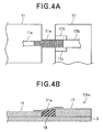
- Fig. 4A and Fig. 4B illustrate an embodiment of the microwave circuit package shown in Fig. 3A and Fig. 3B, in which the dielectric substrate 17 is provided with an impedance regulating stub 17z serving as a high-frequency compensating circuit.
- a high-frequency compensating circuit On the dielectric substrate 17 of a microstrip line 17m for effecting high-frequency inputting and outputting, there is provided a high-frequency compensating circuit in close proximity to the bond position of the ribbon 11e.
- the high-frequency compensating circuit may comprise a bonding pad and be disposed on the MMIC 11.
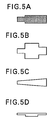
- Fig. 5A - Fig. 5C illustrate various configurations of the microwave circuit ribbon according to the present invention, as seen in top plan, while Fig. 5D shows the ribbon in side elevation.
- Fig. 5A Shown in Fig. 5A is a ribbon corresponding to the ribbons 11e, 12e described in relation to Fig. 1 through Fig. 4 and having a width varied discontinuously.
- the ribbon shown in Fig. 5B has ends equal in width to the ends of the ribbon shown in Fig. 5A, and a central part wider than that of the latter ribbon so that the width of the former ribbon is longitudinally varied discontinuously.
- the ribbon shown in Fig. 5C is continuously varied in width longitudinally but has ends equal in width to the ends of the ribbon shown in Fig. 5A, thus providing a trapezoidal configuration.
- the thickness of the ribbons shown in Fig. 5A - Fig. 5C may be varied so that a stepped portion is provided as shown in Fig. 5D.
- a stepped portion By varying the thickness of the ribbons at portions other than bonding portions thereof to provide such a stepped portion, longitudinal positioning of the ribbons upon bonding thereof becomes easy.
- the ribbons may have thicknesses uniform lengthwise.
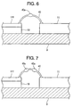
- Fig. 6 illustrates a bonding wire 40 as an example for connecting the high-frequency output and RF terminal 11f of the MMIC 11.
- the bonding wire 40 has a thickness or diameter altered at portions other than the bonding portions thereof.
- the bonding wire has a flattened portion 40a formed, for example, by pinching with a small-sized pair of tweezers.
- the flattened portion 40a has a substantially oval cross-section.
- the bonding wire 40 may be altered in configuration such that it has two flattened portions 40a, 40a at portions other than the bonding portions thereof, as shown in Fig. 7.
- Fig. 8 illustrates an altered form of the bonding wire 40 in which part of the bonding wire 40 is corrugated as at 40b.
- a corrugated portion can be formed, for example, by pinching a desired part of the wire with saw-teethed portions at tip ends of a small-sized pair of tweezers.
- the bonding wire 40 has a thickness varied discontinuously lengthwise such that it has a corrugated portion 40c on one side and a flat or straight portion on the other, the corrugated and straight portions being obtained by causing a desired part of the bonding wire to be pinched between a saw-teethed portion on one side of a tip end and a straight portion on an opposed side of a companion tip end of a pair of tweezers (see Fig. 10).
- Fig. 9 illustrates a still further alteration of the bonding wire 40 in which both a flattened portion 40a and a corrugated portion 40b respectively shown in Fig. 6 and Fig. 8 are provided.
- the RF terminals 11f, 11g, 12f, 12g and high-frequency output ends of the MMICs 11, 12 may be interconnected by means of beam leads of gold or like material, or the ribbons as used at the high-frequency input ends.
- the high-frequency output ends and strip conductor 17b of the MMICs 11, 12 may be interconnected through the above-described inventive bonding wires.
- the RF terminals 11f, 11g, 12f, 12g, 17a may be arranged to extend vertically with respect to the surface of the metallic substrate 3 like the DC terminals 34 - 37.
- the present invention may also be applied to the radar module and antenna apparatus as proposed in European Patent Application No. 96 104 536.6.
- a plurality of MMICs each including four high-frequency field effect transistors (FETs) and two mixers, may be mounted to the package so as to provide a multichip circuit.
- FETs field effect transistors
- the ribbons, bonding wires and/or microwave circuit package employing the same allow intentional alteration or variation of discontinuity of impedance within the microwave circuit in that the width of the ribbons and/or the thickness of the bonding wires are altered at portions other than the bonding portions thereof, whereby the frequency characteristics of the microwave circuit can be varied intentionally by virtue of the ribbons and bonding wires incorporating such intentional alterations.
- impedance in the respective microscopic portions of the ribbons and bonding wires and hence the microwave circuit package according to the present invention can be varied gradually (or continuously).
- impedance in the respective microscopic portions of the ribbons and/or the bonding wires and hence the microwave circuit package according to the present invention can be effectively varied suddenly (or in a phased manner) since the width of the ribbons and/or the thickness of the bonding wires are varied discontinuously.
- the frequency characteristics of the microwave circuits can be varied not only by the ribbons and/or the bonding wires but also by the high-frequency compensating circuit provided for impedance regulation. As a result, it becomes possible to make slight changes in the frequency characteristics of the microwave circuits by means of the high-frequency compensating circuit and the ribbons and/or bonding wires having different characteristics.
- the microwave circuit package according to the present invention employs the inventive ribbons varied in thickness at portions other than the bonding portions thereof, it becomes possible to intentionally vary the discontinuity of impedance in the microwave circuit, thus enabling intentional variation of the frequency characteristics of the microwave circuit.
- the microwave circuit package according to the present invention employs the ribbons varied in width at portions other than the bonding portions thereof, it becomes possible to intentionally vary the discontinuity of impedance in the microwave circuit, thus enabling intentional variation of the frequency characteristics of the microwave circuit.
- the ribbons are provided with opposite ends having widths narrower than the widths of the high-frequency input/output ends of the ribbons at which the latter are to be bonded, positioning of the ribbons upon bonding thereof becomes easy, thereby reducing the production costs of the microwave circuit package.
- the support member supporting the ribbons thereon is disposed on the metallic substrate.
- a sloped surface corresponding to the height difference may be provided on the support member so that the ribbons can be positioned to lie along the sloped surface, thus compensating the height difference.
- the microwave circuit package according to the present invention by intentionally varying the width of the ribbons at portions other than the bonding portions thereof, it becomes possible to intentionally vary the discontinuity of impedance within the microwave circuit, whereby intentional variation of the frequency characteristics of the microwave circuit is enabled.
- the ribbon width at the edges of the MMICs up to the width of the strip conductor it becomes possible to obtain an arrangement similar to the one in which the strip conductor extends up to the high-frequency input/output ends of the MMICs.
- the thus-obtained arrangement provides increased post-mount high-frequency characteristics of the MMICs compared to at least the arrangement in which the ribbons of uniform width equal to the width of the high-frequency input/output ends of the MMICs are used for connection.
- the frequency characteristics of the microwave circuit can be varied via the ribbons. Such frequency variation can also be achieved through impedance regulation using the high-frequency compensating circuit. Thus, subtle or delicate variation of the frequency characteristics of the microwave circuit is enabled by using the ribbons and high-frequency compensating circuit having different characteristics.
- the high-frequency compensating circuit in the microwave circuit package according to the present invention is comprised of the impedance regulating stub disposed in close proximity to the bonding portions of the ribbons and/or the bonding wires, impedance regulation can be effected on the MMIC side, as well as on the dielectric substrate side.
- a ribbon (11e, 12e) and a bonding wire (40, 42) are connected respectively to a high-frequency input and output of a microwave circuit, the width of the ribbon and/or the thickness of the bonding wire being varied continuously or discontinuously at a portion other than a portion used for bonding.
Landscapes
- Waveguide Connection Structure (AREA)
- Waveguides (AREA)
- Microwave Amplifiers (AREA)
- Wire Bonding (AREA)
Abstract
Description
- The present invention relates to an improvement in a microwave circuit package for sealing therein microwave circuitry having monolithic microwave integrated circuits (hereinafter referred to as MMICs), as well as to ribbons and bonding wires for use in fabricating the microwave circuit package.
- Conventionally, bonding wires having uniform diameters along their lengths, ribbons of uniform thickness and/or mesh ribbons, have been used for mounting high-frequency devices to a metallic substrate in a microwave circuit package.
- Japanese Patent Laid-Open Publication No. HEI 1-300546 discloses a microwave circuit package in which electrostatic capacity is provided externally of an area of an MMIC chip by forming a dielectric layer between a metallic substrate and a biasing direct current (DC) terminal.
- In such a microwave circuit package, discontinuity of impedance is likely to arise at places where ribbons and bonding wires are provided. As a result, it is likely that components such as MMICs vary in their bare characteristics after mounting or assemblage thereof, leading to deteriorated characteristics of the components.
- Certain occasions arise wherein it is desired that a microwave circuit package be fabricated using metallic substrates, MMICs and bonding wires which are altered in their materials, while rendering the microwave circuit package to be compatible with a separate microwave circuit package fabricated using the same components but not involving such changes in material, by varying the post-mounting high-frequency characteristics of the MMIC and so forth.
- The post-mounting high-frequency characteristics of the MMICs may be varied by changing the lengths of the ribbons and bonding wires. However, connection through the bonding wires requires of the latter to be gently curved in a proper manner. In addition, length alteration of the bonding wires is limited due to the limited space within the microwave circuit package. Another possible approach would be to change the spacing between the components such as the MMICs to allow alteration of the lengths of the ribbons. However, the space alteration is also limited and hence is not an effective solution.
- It is an object of the present invention to provide a ribbon and a bonding wire which can be connected to an input and an output of a microwave circuit and allow intentional variation of the frequency characteristics of the microwave circuit.
- Another object of the present invention is to provide a microwave circuit package having a metallic substrate and sealing therein an MMIC mounted to the metallic substrate, the microwave circuit package further comprising a circuit or circuit element having a ribbon and/or a bonding wire assembled thereinto for allowing intentional variation of the frequency characteristics of the resulting microwave circuit.
- According to the present invention, there are provided a ribbon and a bonding wire, the width and thickness of which are varied at at least a portion other than a portion thereof used for bonding. Specifically, the ribbon width and bonding wire thickness may be varied continuously or discontinuously. The ribbon and bonding wire involving such variation may be used for the connection of a high-frequency input/output of a microwave circuit sealed in a microwave circuit package.
- Effects resulting from the variation of the ribbon width and bonding wire thickness at portions other than portions thereof used for bonding may be explained as below:
- The ribbon and bonding wire have such components as resistance R and reactance X, as well as the total opposition, namely, impedance Z which is a combination of the former two. Using resistance R and reactance X, the correlations may be represented by


- Reactance X is a function of frequency f (or angular frequency

- Accordingly, by varying the width of the ribbon and the thickness of the bonding wire at portions other than portions thereof used for bonding, it becomes possible to intentionally vary the discontinuity of impedance within a microwave circuit and to thus vary the frequency characteristics of the microwave circuit.
- Consequently, it also becomes possible to vary impedance in the respective microscopic portions of the ribbon and bonding wire gradually (or continuously) by continuously varying the ribbon width and bonding wire thickness.
- By varying the ribbon width and bonding wire thickness discontinuously, it becomes possible to vary impedance in the respective microscopic portions of the ribbon and bonding wire suddenly (or in a phased fashion).
- In a preferred form, the MMIC sealed within the microwave circuit package according to the present invention is provided with a high-frequency compensating circuit positioned closely to the bonding portions of the ribbon and bonding wire. Apart from varying the frequency characteristics of the microwave circuit through the variation of the ribbon width and bonding wire thickness, provision of such a high-frequency compensating circuit also makes it possible to independently vary the frequency characteristics of the microwave circuit in that impedance can be regulated using the high-frequency compensating circuit. The high-frequency compensating circuit may be comprised of an impedance regulating stub. As a result, it become possible to delicately vary the frequency characteristics of the microwave circuit using the ribbon, bonding wire and the high-frequency compensating circuit having different characteristics.
- Alternatively, the high-frequency input/output of the microwave circuit within the microwave circuit package may be connected by means of the ribbon varied in thickness at at least a portion other than a portion thereof used for bonding. By varying the thickness of the ribbon at a portion other than a portion thereof used for bonding, it becomes possible to intentionally vary the discontinuity of impedance within the microwave circuit so as to effect the intentional variation of the frequency characteristics of the microwave circuit.
- The high-frequency input/output of the microwave circuit within the microwave circuit package according to the present invention may desirably be connected by means of the ribbon varied in width at a portion other than a portion thereof used for bonding and having opposed ends narrower than the widths of the microwave circuit high-frequency input/output ends to which the ribbon is to be bonded. By varying the width of the ribbon at a portion other than a portion thereof used for bonding, it becomes possible to intentionally vary the discontinuity of impedance in the microwave circuit to thereby intentionally vary the frequency characteristics of the microwave circuit. By making the widths of the opposed ribbon ends narrower than the widths of the high-frequency input/output ends to which the ribbon is to be bonded, positioning of the ribbon upon bonding thereof becomes easy, leading to reduced production costs of the microwave circuit package.
- The microwave circuit package according to the present invention includes a support member disposed on the metallic substrate for supporting the ribbon thereon. By disposing the support member on the metallic substrate for supporting the ribbon, increased mechanical strength may be imparted to the ribbon, thus resulting in increased reliability of the microwave circuit. When there is a height difference between the MMICs and other components, a sloped surface corresponding to the height difference may be provided on the support member so that the ribbon can be positioned to lie along the sloped surface, thus compensating for the height difference. Further, by varying the material of the support member, it becomes possible to vary capacitance between the ribbon and metallic substrate. This also enables the variation of the frequency characteristics of the microwave circuit.
- The ribbon may have a width enlarged at an edge of the MMIC to the width of the strip conductor while the opposed ends thereof are arranged such that the one proximate to the MMIC has a width substantially equal to the width of the high-frequency input of the MMIC and the other proximate to the dielectric substrate has a width substantially equal to the width of the strip conductor. By varying the width of the ribbon at a portion other than a portion thereof used for bonding, it becomes possible to intentionally vary the discontinuity of impedance within the microwave circuit and hence the frequency characteristics of the microwave circuit. Particularly, by increasing the width of the ribbon at an edge of the MMIC to the width of the strip conductor, it becomes possible to obtain an arrangement similar to the arrangement in which the strip conductor extends to the high-frequency input/output ends of the MMIC. The thus obtained arrangement produces improved post-mounting frequency characteristics compared to at least the arrangement wherein the ribbon of uniform width equal to the widths of the high frequency input/output ends of the MMIC is used for connection.
- Preferably, the microwave circuit package according to the present invention includes a high-frequency compensating circuit disposed on the dielectric substrate proximately to the bonding portion of the ribbon. Apart from varying the frequency characteristics of the microwave circuit through the use of the ribbon, provision of such a high-frequency compensating circuit also enables independent variation of the frequency characteristics of the microwave circuit in that impedance can be regulated through the use of the high-frequency compensating circuit. As a result, it become possible to delicately vary the frequency characteristics of the microwave circuit through the use of the ribbon and the high-frequency compensating circuit having different characteristics.
- Preferred embodiments of the present invention will be described in more detail hereinbelow with reference to the accompanying drawings, in which:
- Fig. 1 is a schematic plan view illustrating a microwave circuit package according to the present invention;
- Fig. 2 is a schematic cross-sectional view taken along line A - A of Fig. 1, showing the microwave circuit package with DC terminals and bonding wires removed;
- Fig. 3A is an enlarged plan view illustrating an MMIC with its high-frequency input connected to a strip conductor on a dielectric substrate by means of a ribbon;
- Fig. 3B is a schematic cross-sectional view of Fig. 3A;
- Fig. 4A is an enlarged plan view similar to Fig. 3A illustrating a high-frequency compensating circuit disposed on the dielectric substrate;
- Fig. 4B is a schematic cross-sectional view of Fig. 4A;
- Fig. 5A - Fig. 5D schematically illustrate various ribbon configurations;
- Fig. 6 is a view illustrating schematically a bonding wire having a flattened portion;
- Fig. 7 is a view illustrating schematically a bonding wire having two flattened portions;
- Fig. 8 is a view schematically illustrating a bonding wire with a corrugated portion;
- Fig. 9 is a view schematically illustrating a bonding wire having a flattened portion and a corrugated portion; and
- Fig. 10 is a view schematically illustrating a bonding sire with a corrugated portion on one surface thereof.
- Referring to Figs. 1 and 2, a
microwave circuit package 10 according to the present invention includes ametallic substrate 3 and seals monolithic microwave integrated circuits (MMICs) 11, 12 disposed on themetallic substrate 3. - The
metallic substrate 3 also seals adielectric substrate 17 anddielectric elements metallic substrate 3. Thedielectric substrate 17 is provided on a surface thereof with astrip conductor 17b. Themetallic substrate 3,dielectric substrate 17 andstrip conductor 17b jointly provide microstrip lines. - The
metallic substrate 3 is formed from Kovar or the like and also serves as a heat sink. Anupper cover 6 is formed from a dielectric material. TheMMICs dielectric substrate 17 is formed from ceramics such as alumina ceramics. - The
MMIC 11 has a plurality of biasingDC terminals respective bonding wires metallic substrate 3 in an electrically insulated manner for supplying a given biasing voltage to theMMIC 11. - Similarly, the
MMIC 12 has a plurality of biasingDC terminals respective bonding wires metallic substrate 3 in an electrically insulated manner for supplying a given biasing voltage to theMMIC 12. - High-frequency input of the
MMIC 11 is connected to thestrip conductor 17b on thedielectric substrate 17 by means of aribbon 11e. High-frequency outputs of theMMIC 11 are connected to theirrespective RF terminals bonding wires - High-frequency input of the
MMIC 12 is connected to thestrip conductor 17b on thedielectric substrate 17 via aribbon 12e. Two high-frequency outputs of theMMIC 12 are connected to theirrespective RF terminals bonding wires - The
strip conductor 17b and RF terminal 17a on thedielectric substrate 17 are interconnected through abonding wire 44. - Using the above-described microstrip lines, various circuits and/or circuit elements may be fabricated. For example, a distributor for distributing high-frequency signals can be formed using such microstrip lines to thereby reduce the RF terminals in number.
- With the DC terminals 34 - 37 being arranged to extend vertically relative to the surface of the
metallic substrate 3 andRF terminals metallic substrate 3 and extending horizontally within a plane of the surface of thebase plate 3, themicrowave circuit package 10 can be placed in close proximity to a companion microwave circuit package, whereby highly dense microwave circuit package assemblage is enabled. - Fig. 3A illustrates in top plan a
ribbon 11e connecting the high-frequency input terminal 11s of theMMIC 11, forming part of the lines, with thestrip conductor 17b on thedielectric substrate 17, and its peripheries. Fig. 3B is a cross-sectional view illustrating theribbon 11e and its peripheries. Theribbon 11e is supported on asupport member 18 which is formed of a material such as resins and disposed on themetallic substrate 3. - Ends of the
ribbon 11e are bonded respectively to the high-frequency input 11s andstrip conductor 17b by thermal pressure bonding or ultrasonic pressure bonding. The width of the ribbon end on theMMIC 11 side is equal to the width of the high-frequency input 11s while the ribbon end on thedielectric substrate 17 side is equal to the width of thestrip conductor 17b. The width of theribbon 11e increased at the edge of theMMIC 11 to correspond to the width of thestrip conductor 17b. Stated otherwise, theribbon 11e has altered or varied widths at portions other than the portions to be subjected to bonding. Alternatively, the ribbon width on theMMIC 11 side may be smaller than the width of the high-frequency input 11s whilst the ribbon end on thedielectric substrate 17 side may be smaller than the width of thestrip conductor 17b. That is, the end widths of theribbon 11e may be smaller than the widths of the high-frequency input and output ends to which theribbon 11e is to be bonded. - Fig. 4A and Fig. 4B illustrate an embodiment of the microwave circuit package shown in Fig. 3A and Fig. 3B, in which the
dielectric substrate 17 is provided with animpedance regulating stub 17z serving as a high-frequency compensating circuit. On thedielectric substrate 17 of amicrostrip line 17m for effecting high-frequency inputting and outputting, there is provided a high-frequency compensating circuit in close proximity to the bond position of theribbon 11e. The high-frequency compensating circuit may comprise a bonding pad and be disposed on theMMIC 11. - Fig. 5A - Fig. 5C illustrate various configurations of the microwave circuit ribbon according to the present invention, as seen in top plan, while Fig. 5D shows the ribbon in side elevation.
- Shown in Fig. 5A is a ribbon corresponding to the
ribbons - The ribbon shown in Fig. 5B has ends equal in width to the ends of the ribbon shown in Fig. 5A, and a central part wider than that of the latter ribbon so that the width of the former ribbon is longitudinally varied discontinuously.
- The ribbon shown in Fig. 5C is continuously varied in width longitudinally but has ends equal in width to the ends of the ribbon shown in Fig. 5A, thus providing a trapezoidal configuration.
- The thickness of the ribbons shown in Fig. 5A - Fig. 5C may be varied so that a stepped portion is provided as shown in Fig. 5D. By varying the thickness of the ribbons at portions other than bonding portions thereof to provide such a stepped portion, longitudinal positioning of the ribbons upon bonding thereof becomes easy. Alternatively, the ribbons may have thicknesses uniform lengthwise.
- Fig. 6 illustrates a
bonding wire 40 as an example for connecting the high-frequency output and RF terminal 11f of theMMIC 11. - As shown in Fig. 6, the
bonding wire 40 has a thickness or diameter altered at portions other than the bonding portions thereof. The bonding wire has a flattenedportion 40a formed, for example, by pinching with a small-sized pair of tweezers. The flattenedportion 40a has a substantially oval cross-section. Thebonding wire 40 may be altered in configuration such that it has two flattenedportions - Fig. 8 illustrates an altered form of the
bonding wire 40 in which part of thebonding wire 40 is corrugated as at 40b. Such a corrugated portion can be formed, for example, by pinching a desired part of the wire with saw-teethed portions at tip ends of a small-sized pair of tweezers. - In a further altered form, the
bonding wire 40 has a thickness varied discontinuously lengthwise such that it has a corrugatedportion 40c on one side and a flat or straight portion on the other, the corrugated and straight portions being obtained by causing a desired part of the bonding wire to be pinched between a saw-teethed portion on one side of a tip end and a straight portion on an opposed side of a companion tip end of a pair of tweezers (see Fig. 10). - Fig. 9 illustrates a still further alteration of the
bonding wire 40 in which both a flattenedportion 40a and acorrugated portion 40b respectively shown in Fig. 6 and Fig. 8 are provided. - The
RF terminals MMICs strip conductor 17b of theMMICs RF terminals metallic substrate 3 like the DC terminals 34 - 37. - The present invention may also be applied to the radar module and antenna apparatus as proposed in European Patent Application No. 96 104 536.6. For example, a plurality of MMICs, each including four high-frequency field effect transistors (FETs) and two mixers, may be mounted to the package so as to provide a multichip circuit.
- As thus far explained, the ribbons, bonding wires and/or microwave circuit package employing the same according to the present invention allow intentional alteration or variation of discontinuity of impedance within the microwave circuit in that the width of the ribbons and/or the thickness of the bonding wires are altered at portions other than the bonding portions thereof, whereby the frequency characteristics of the microwave circuit can be varied intentionally by virtue of the ribbons and bonding wires incorporating such intentional alterations.
- Also, impedance in the respective microscopic portions of the ribbons and bonding wires and hence the microwave circuit package according to the present invention can be varied gradually (or continuously).
- Further, impedance in the respective microscopic portions of the ribbons and/or the bonding wires and hence the microwave circuit package according to the present invention can be effectively varied suddenly (or in a phased manner) since the width of the ribbons and/or the thickness of the bonding wires are varied discontinuously.
- Additionally, in the microwave circuit package according to the present invention, the frequency characteristics of the microwave circuits can be varied not only by the ribbons and/or the bonding wires but also by the high-frequency compensating circuit provided for impedance regulation. As a result, it becomes possible to make slight changes in the frequency characteristics of the microwave circuits by means of the high-frequency compensating circuit and the ribbons and/or bonding wires having different characteristics.
- Since the microwave circuit package according to the present invention employs the inventive ribbons varied in thickness at portions other than the bonding portions thereof, it becomes possible to intentionally vary the discontinuity of impedance in the microwave circuit, thus enabling intentional variation of the frequency characteristics of the microwave circuit.
- Also, since the microwave circuit package according to the present invention employs the ribbons varied in width at portions other than the bonding portions thereof, it becomes possible to intentionally vary the discontinuity of impedance in the microwave circuit, thus enabling intentional variation of the frequency characteristics of the microwave circuit. In particular, since the ribbons are provided with opposite ends having widths narrower than the widths of the high-frequency input/output ends of the ribbons at which the latter are to be bonded, positioning of the ribbons upon bonding thereof becomes easy, thereby reducing the production costs of the microwave circuit package.
- Furthermore, in the microwave circuit package according to the present invention, the support member supporting the ribbons thereon is disposed on the metallic substrate. As a result, it becomes possible to impart mechanical strength to the ribbons, thus resulting in increased reliability of the microwave circuit. When there is a height difference between the high-frequency inputting/outputting MMICs or the like, a sloped surface corresponding to the height difference may be provided on the support member so that the ribbons can be positioned to lie along the sloped surface, thus compensating the height difference. By altering the material of the support member, it also becomes possible to vary the capacitance between the ribbons and the metallic substrate. Utilization of this further enables varying of the frequency characteristics of the microwave circuit.
- In the microwave circuit package according to the present invention, by intentionally varying the width of the ribbons at portions other than the bonding portions thereof, it becomes possible to intentionally vary the discontinuity of impedance within the microwave circuit, whereby intentional variation of the frequency characteristics of the microwave circuit is enabled. Particularly, by increasing the ribbon width at the edges of the MMICs up to the width of the strip conductor, it becomes possible to obtain an arrangement similar to the one in which the strip conductor extends up to the high-frequency input/output ends of the MMICs. The thus-obtained arrangement provides increased post-mount high-frequency characteristics of the MMICs compared to at least the arrangement in which the ribbons of uniform width equal to the width of the high-frequency input/output ends of the MMICs are used for connection.
- As already explained above, in the microwave circuit package according to the present invention, the frequency characteristics of the microwave circuit can be varied via the ribbons. Such frequency variation can also be achieved through impedance regulation using the high-frequency compensating circuit. Thus, subtle or delicate variation of the frequency characteristics of the microwave circuit is enabled by using the ribbons and high-frequency compensating circuit having different characteristics.
- Moreover, since the high-frequency compensating circuit in the microwave circuit package according to the present invention is comprised of the impedance regulating stub disposed in close proximity to the bonding portions of the ribbons and/or the bonding wires, impedance regulation can be effected on the MMIC side, as well as on the dielectric substrate side.
- The foregoing discussion discloses and describes merely exemplary embodiments of the present invention. One skilled in the art will readily recognize from such discussion, and from the accompanying drawings and claims, that various changes, modifications and variations can be made therein without departing from the spirit and scope of the invention as defined in the following claims.
- A ribbon (11e, 12e) and a bonding wire (40, 42) are connected respectively to a high-frequency input and output of a microwave circuit, the width of the ribbon and/or the thickness of the bonding wire being varied continuously or discontinuously at a portion other than a portion used for bonding. By applying the ribbon and bonding wire to a microwave circuit package (10) including a metallic substrate (3) and sealing therein an MMIC (11, 12) mounted to the metallic substrate, desired high-frequency characteristics of the MMIC can be obtained.
Claims (18)
- A ribbon designed to be connected to a high-frequency input of a microwave circuit, wherein said ribbon (11e, 12e) has a varied width at at least a portion other than a portion thereof to be used for bonding.
- The ribbon of Claim 1, wherein the varied width of said ribbon is continuous.
- The ribbon of Claim 1, wherein the varied width of said ribbon is discontinuous.
- A bonding wire designed to be connected to a high-frequency output of a microwave circuit, wherein said bonding wire (40, 42) has a varied thickness at at least a portion other than a portion thereof used for bonding.
- The bonding wire of Claim 4, wherein the varied thickness of said bonding wire is continuous.
- The bonding wire of Claim 4, wherein the varied thickness of said bonding wire is discontinuous.
- A microwave circuit package including a metallic substrate (3) and sealing therein an MMIC (11, 12) mounted to said metallic substrate (3), said microwave circuit package (10) further comprising:a ribbon (11e, 12e) connected to a high-frequency input of said microwave circuit (10); anda bonding wire (40, 42) connected to a high-frequency output of said microwave circuit (10), the width of said ribbon and/or the thickness of said bonding wire being varied at at least a portion other than a bonding portion thereof.
- The microwave circuit package of Claim 7, wherein the variation of the ribbon width and/or the bonding wire thickness is continuous.
- The microwave circuit package of Claim 7, wherein the variation of the ribbon width and/or the bonding wire thickness is discontinuous.
- The microwave circuit package of Claim 7, 8 or 9, wherein said MMIC for inputting/outputting a high frequency includes a high-frequency compensating circuit (17z) disposed proximately to the bonding portions of said ribbon and/or said bonding wire.
- The microwave circuit package of Claim 10, wherein said high-frequency compensating circuit comprises an impedance regulating stub (17z).
- A microwave circuit package (10) including a metallic substrate (3) and sealing therein an MMIC (11, 12) mounted to said metallic substrate (3), said microwave circuit package (10) further comprising:a ribbon (11e, 12e) connected to a high-frequency input of said microwave circuit, the thickness of said ribbon being varied at at least a portion other than a bonding portion thereof.
- The microwave circuit package of Claim 12, further comprising a support member (18) disposed on said metallic substrate (3) for supporting said ribbon thereon.
- A microwave circuit package (10) including a metallic substrate (3) and sealing therein an MMIC (11, 12) mounted to said metallic substrate (3), said microwave circuit package (10) further comprising:a ribbon (11e, 12e) connected to a high-frequency input of said microwave circuit, the width of said ribbon being varied at at least a portion other than a bonding portion thereof, said ribbon having opposed ends of a width narrower than the width of the high-frequency input to which said ribbon is to be bonded.
- The microwave circuit package of Claim 14, further comprising a support member disposed on said metallic substrate for supporting said ribbon thereon.
- A microwave circuit package (10) including a metallic substrate (3) and sealing therein an MMIC (11, 12) mounted to said metallic substrate (3), said microwave circuit package (10) further comprising:a dielectric substrate (17) having a strip conductor (17b) and mounted to said metallic substrate in a sealed fashion; anda ribbon (11e, 12e) connected to a high-frequency input of said microwave circuit,said ribbon having opposed ends, one of said opposed ends proximate to said MMIC having a width substantially equal to the width of said high-frequency input of said MMIC and the other of said opposed ends proximate to said dielectric substrate having a width substantially equal to the width of said strip conductor,the ribbon width at an edge of said MMIC being enlarged to the width of said strip conductor.
- The microwave circuit package of Claim 16, further comprising a high-frequency compensating circuit (17z) disposed on said dielectric substrate in close proximity to the bonding portion of said ribbon.
- The microwave circuit package of Claim 17, wherein said high-frequency compensating circuit comprises an impedance regulating stub (17z).
Applications Claiming Priority (3)
| Application Number | Priority Date | Filing Date | Title |
|---|---|---|---|
| JP102814/96 | 1996-04-24 | ||
| JP8102814A JPH09289404A (en) | 1996-04-24 | 1996-04-24 | Ribbon, bonding wire and microwave circuit package |
| JP10281496 | 1996-04-24 |
Publications (3)
| Publication Number | Publication Date |
|---|---|
| EP0803907A2 true EP0803907A2 (en) | 1997-10-29 |
| EP0803907A3 EP0803907A3 (en) | 1999-07-28 |
| EP0803907B1 EP0803907B1 (en) | 2007-12-05 |
Family
ID=14337510
Family Applications (1)
| Application Number | Title | Priority Date | Filing Date |
|---|---|---|---|
| EP97105797A Expired - Lifetime EP0803907B1 (en) | 1996-04-24 | 1997-04-08 | Method of regulating the impedance of a microwave circuit package |
Country Status (4)
| Country | Link |
|---|---|
| US (2) | US5936492A (en) |
| EP (1) | EP0803907B1 (en) |
| JP (1) | JPH09289404A (en) |
| DE (1) | DE69738340T2 (en) |
Cited By (2)
| Publication number | Priority date | Publication date | Assignee | Title |
|---|---|---|---|---|
| WO2000038232A1 (en) * | 1998-12-22 | 2000-06-29 | Telefonaktiebolaget Lm Ericsson (Publ) | Wire bond compensation |
| US8829659B2 (en) | 2009-08-12 | 2014-09-09 | Sony Corporation | Integrated circuit |
Families Citing this family (24)
| Publication number | Priority date | Publication date | Assignee | Title |
|---|---|---|---|---|
| JP3209183B2 (en) * | 1998-07-08 | 2001-09-17 | 日本電気株式会社 | High frequency signal integrated circuit package and method of manufacturing the same |
| US6664630B2 (en) * | 2001-10-16 | 2003-12-16 | Hitachi Maxell, Ltd. | Semiconductor device |
| JP3756129B2 (en) * | 2002-06-11 | 2006-03-15 | Necトーキン株式会社 | Transmission line type noise filter |
| US6737931B2 (en) * | 2002-07-19 | 2004-05-18 | Agilent Technologies, Inc. | Device interconnects and methods of making the same |
| TW550990B (en) * | 2002-10-24 | 2003-09-01 | Advanced Semiconductor Eng | A printed circuit board |
| JP2005072031A (en) * | 2003-08-22 | 2005-03-17 | Renesas Technology Corp | High-frequency semiconductor device, communication electronic component, and wireless communication system |
| WO2005048314A2 (en) * | 2003-11-12 | 2005-05-26 | Silicon Pipe, Inc. | Tapered dielectric and conductor structures and applications thereof |
| US20050248022A1 (en) * | 2004-05-10 | 2005-11-10 | Northern Microdesign, Inc. | High data rate chip mounting |
| DE112005001218A5 (en) * | 2004-06-25 | 2007-05-24 | Conti Temic Microelectronic Gmbh | Electrical assembly with a protective cover |
| US7397329B2 (en) * | 2004-11-02 | 2008-07-08 | Du Toit Nicolaas D | Compact tunable filter and method of operation and manufacture therefore |
| US7471520B2 (en) * | 2005-03-10 | 2008-12-30 | Avago Technologies Fiber Ip (Singapore) Pte. Ltd. | Impedance matching external component connections with uncompensated leads |
| US7388451B2 (en) * | 2005-08-15 | 2008-06-17 | Northrop Grumman Corporation | Thickness tapered substrate launch |
| US7295084B2 (en) * | 2005-09-28 | 2007-11-13 | Agilent Technologies, Inc. | Electrical interconnection for coaxial line to slab line structure including a bead ring |
| US7443018B2 (en) * | 2005-11-09 | 2008-10-28 | Stats Chippac Ltd. | Integrated circuit package system including ribbon bond interconnect |
| US7557431B2 (en) * | 2007-01-18 | 2009-07-07 | Miteq, Inc. | Microwave surface mount hermetically sealed package and method of forming the same |
| DE102007008464B4 (en) * | 2007-02-19 | 2012-01-05 | Hottinger Baldwin Messtechnik Gmbh | Optical strain gauge |
| JP4656212B2 (en) * | 2008-06-13 | 2011-03-23 | ソニー株式会社 | Connection method |
| TW201352092A (en) | 2012-03-28 | 2013-12-16 | Fujikura Ltd | Wiring board |
| US20130265734A1 (en) * | 2012-04-04 | 2013-10-10 | Texas Instruments Incorporated | Interchip communication using embedded dielectric and metal waveguides |
| US20130265733A1 (en) * | 2012-04-04 | 2013-10-10 | Texas Instruments Incorporated | Interchip communication using an embedded dielectric waveguide |
| CN102856302B (en) * | 2012-09-14 | 2014-11-05 | 中国科学院半导体研究所 | Three-dimensional packaging device for photonic integrated chip matching circuit |
| FR3015781B1 (en) * | 2013-12-20 | 2016-02-05 | Thales Sa | HYPERFREQUENCY INTERCONNECTION DEVICE |
| KR102298516B1 (en) * | 2020-02-28 | 2021-09-27 | 주식회사 웨이브피아 | Lead frame of hermetic RF chip package for incorporating the function of impedance matching |
| KR102298517B1 (en) * | 2020-02-28 | 2021-09-06 | 주식회사 웨이브피아 | Lead frame of RF chip package for incorporating the function of impedance matching |
Family Cites Families (25)
| Publication number | Priority date | Publication date | Assignee | Title |
|---|---|---|---|---|
| JPS5575301A (en) * | 1978-12-01 | 1980-06-06 | Hitachi Denshi Ltd | Amplitude frequency characteristics compensating circuit at microwave band |
| JPS5939055A (en) * | 1982-08-26 | 1984-03-03 | Sanken Electric Co Ltd | Manufacture of semiconductor device |
| US4600907A (en) * | 1985-03-07 | 1986-07-15 | Tektronix, Inc. | Coplanar microstrap waveguide interconnector and method of interconnection |
| JPS63131970A (en) * | 1986-11-21 | 1988-06-03 | 松下冷機株式会社 | Forced cooling device for refrigerator |
| JPS6431567A (en) | 1987-07-27 | 1989-02-01 | Honda Motor Co Ltd | Production of fiber reinforced metallic member |
| US4967261A (en) * | 1987-07-30 | 1990-10-30 | Mitsubishi Denki Kabushiki Kaisha | Tape carrier for assembling an IC chip on a substrate |
| JPH01315167A (en) * | 1988-03-01 | 1989-12-20 | Oki Electric Ind Co Ltd | Semiconductor device |
| JPH01293001A (en) * | 1988-05-20 | 1989-11-27 | Fujitsu Ltd | Connecting structure for micro-strip line |
| JPH01300546A (en) | 1988-05-30 | 1989-12-05 | Sharp Corp | Packaging stem for semiconductor device |
| JPH02185047A (en) * | 1989-01-12 | 1990-07-19 | Nec Corp | Semiconductor device |
| JPH02237301A (en) * | 1989-03-10 | 1990-09-19 | Nec Corp | Coaxial microstrip line converter |
| JPH03131102A (en) * | 1989-10-17 | 1991-06-04 | Mitsubishi Materials Corp | Method for connecting semiconductor element and circuit board or carrier |
| JPH07105608B2 (en) * | 1990-03-01 | 1995-11-13 | 三菱電機株式会社 | Microwave integrated circuit storage case |
| US5086335A (en) * | 1990-07-31 | 1992-02-04 | Hewlett-Packard Company | Tape automated bonding system which facilitate repair |
| JPH04180401A (en) * | 1990-11-15 | 1992-06-26 | Hitachi Ltd | High frequency transmission line |
| JPH04212501A (en) * | 1990-12-06 | 1992-08-04 | Fujitsu Ltd | Method of connecting microstrip lines |
| JPH04284661A (en) * | 1991-03-13 | 1992-10-09 | Toshiba Corp | Semiconductor device |
| US5296744A (en) * | 1991-07-12 | 1994-03-22 | Vlsi Technology, Inc. | Lead frame assembly and method for wiring same |
| US5438305A (en) * | 1991-08-12 | 1995-08-01 | Hitachi, Ltd. | High frequency module including a flexible substrate |
| JPH06188603A (en) * | 1992-12-21 | 1994-07-08 | Mitsubishi Electric Corp | Microwave circuit |
| US5395227A (en) | 1993-08-20 | 1995-03-07 | Westinghouse Electric Corporation | Adjustable powder flow gate for a rotary pellet press |
| US5821457A (en) * | 1994-03-11 | 1998-10-13 | The Panda Project | Semiconductor die carrier having a dielectric epoxy between adjacent leads |
| US5491302A (en) * | 1994-09-19 | 1996-02-13 | Tessera, Inc. | Microelectronic bonding with lead motion |
| JP2782053B2 (en) * | 1995-03-23 | 1998-07-30 | 本田技研工業株式会社 | Radar module and antenna device |
| US5736784A (en) * | 1996-10-31 | 1998-04-07 | Hewlett-Packard Co. | Variable-width lead interconnection structure and method |
-
1996
- 1996-04-24 JP JP8102814A patent/JPH09289404A/en active Pending
-
1997
- 1997-04-08 DE DE69738340T patent/DE69738340T2/en not_active Expired - Lifetime
- 1997-04-08 EP EP97105797A patent/EP0803907B1/en not_active Expired - Lifetime
- 1997-04-22 US US08/844,921 patent/US5936492A/en not_active Expired - Lifetime
-
1999
- 1999-07-15 US US09/354,213 patent/US6331806B1/en not_active Expired - Fee Related
Cited By (3)
| Publication number | Priority date | Publication date | Assignee | Title |
|---|---|---|---|---|
| WO2000038232A1 (en) * | 1998-12-22 | 2000-06-29 | Telefonaktiebolaget Lm Ericsson (Publ) | Wire bond compensation |
| US6399894B1 (en) | 1998-12-22 | 2002-06-04 | Telefonaktiebolaget Lm Ericsson (Publ) | Wire bond compensation |
| US8829659B2 (en) | 2009-08-12 | 2014-09-09 | Sony Corporation | Integrated circuit |
Also Published As
| Publication number | Publication date |
|---|---|
| JPH09289404A (en) | 1997-11-04 |
| EP0803907A3 (en) | 1999-07-28 |
| EP0803907B1 (en) | 2007-12-05 |
| DE69738340T2 (en) | 2008-04-03 |
| US5936492A (en) | 1999-08-10 |
| US6331806B1 (en) | 2001-12-18 |
| DE69738340D1 (en) | 2008-01-17 |
Similar Documents
| Publication | Publication Date | Title |
|---|---|---|
| US5936492A (en) | Ribbon, bonding wire and microwave circuit package | |
| EP0798782B1 (en) | Microwave circuit package | |
| US5014115A (en) | Coplanar waveguide semiconductor package | |
| US5677570A (en) | Semiconductor integrated circuit devices for high-speed or high frequency | |
| US5218230A (en) | Ic package with electric conductor lines in dielectric package body | |
| US6414387B1 (en) | Semiconductor device including a chip having high-frequency circuit blocks | |
| US5901042A (en) | Package and semiconductor device | |
| US6906406B2 (en) | Multiple dice package | |
| JP3741274B2 (en) | Semiconductor device | |
| JP2001036309A (en) | Multi-chip module connection structure | |
| US5399906A (en) | High-frequency hybrid semiconductor integrated circuit structure including multiple coupling substrate and thermal dissipator | |
| JPH07263581A (en) | SMD container made of synthetic resin for semiconductor chips | |
| US11935848B2 (en) | Package for a semiconductor device | |
| US4340901A (en) | Lead connecting structure for a semiconductor device | |
| KR100190213B1 (en) | Semiconductor device free from short-circuit due to resin pressure in mold | |
| JPH02198158A (en) | Semiconductor device | |
| JP7718030B2 (en) | semiconductor devices | |
| JP2001144510A (en) | Characteristic adjustment circuit and characteristic adjustment method for microwave circuit | |
| JP2000323907A (en) | Microwave IC connection line | |
| JP2590686B2 (en) | Hybrid integrated circuit | |
| KR19980063740A (en) | Multilayer Leadframe for Molded Packages | |
| JPH066512Y2 (en) | Integrated circuit package | |
| JPS61184852A (en) | Integrated circuit package | |
| JPH0334911Y2 (en) | ||
| JPH07105463B2 (en) | Package for ultra high frequency devices |
Legal Events
| Date | Code | Title | Description |
|---|---|---|---|
| PUAI | Public reference made under article 153(3) epc to a published international application that has entered the european phase |
Free format text: ORIGINAL CODE: 0009012 |
|
| AK | Designated contracting states |
Kind code of ref document: A2 Designated state(s): DE FR GB |
|
| PUAL | Search report despatched |
Free format text: ORIGINAL CODE: 0009013 |
|
| AK | Designated contracting states |
Kind code of ref document: A3 Designated state(s): DE FR GB |
|
| 17P | Request for examination filed |
Effective date: 19991209 |
|
| 17Q | First examination report despatched |
Effective date: 20051025 |
|
| RTI1 | Title (correction) |
Free format text: METHOD OF REGULATING THE IMPEDANCE OF A MICROWAVE CIRCUIT PACKAGE |
|
| GRAP | Despatch of communication of intention to grant a patent |
Free format text: ORIGINAL CODE: EPIDOSNIGR1 |
|
| GRAS | Grant fee paid |
Free format text: ORIGINAL CODE: EPIDOSNIGR3 |
|
| GRAA | (expected) grant |
Free format text: ORIGINAL CODE: 0009210 |
|
| AK | Designated contracting states |
Kind code of ref document: B1 Designated state(s): DE FR GB |
|
| REG | Reference to a national code |
Ref country code: GB Ref legal event code: FG4D |
|
| REF | Corresponds to: |
Ref document number: 69738340 Country of ref document: DE Date of ref document: 20080117 Kind code of ref document: P |
|
| EN | Fr: translation not filed | ||
| PLBE | No opposition filed within time limit |
Free format text: ORIGINAL CODE: 0009261 |
|
| STAA | Information on the status of an ep patent application or granted ep patent |
Free format text: STATUS: NO OPPOSITION FILED WITHIN TIME LIMIT |
|
| 26N | No opposition filed |
Effective date: 20080908 |
|
| PGFP | Annual fee paid to national office [announced via postgrant information from national office to epo] |
Ref country code: GB Payment date: 20080409 Year of fee payment: 12 |
|
| PG25 | Lapsed in a contracting state [announced via postgrant information from national office to epo] |
Ref country code: FR Free format text: LAPSE BECAUSE OF FAILURE TO SUBMIT A TRANSLATION OF THE DESCRIPTION OR TO PAY THE FEE WITHIN THE PRESCRIBED TIME-LIMIT Effective date: 20081003 |
|
| GBPC | Gb: european patent ceased through non-payment of renewal fee |
Effective date: 20090408 |
|
| PG25 | Lapsed in a contracting state [announced via postgrant information from national office to epo] |
Ref country code: GB Free format text: LAPSE BECAUSE OF NON-PAYMENT OF DUE FEES Effective date: 20090408 |
|
| PGFP | Annual fee paid to national office [announced via postgrant information from national office to epo] |
Ref country code: DE Payment date: 20100430 Year of fee payment: 14 |
|
| REG | Reference to a national code |
Ref country code: DE Ref legal event code: R119 Ref document number: 69738340 Country of ref document: DE |
|
| REG | Reference to a national code |
Ref country code: DE Ref legal event code: R119 Ref document number: 69738340 Country of ref document: DE |
|
| PG25 | Lapsed in a contracting state [announced via postgrant information from national office to epo] |
Ref country code: DE Free format text: LAPSE BECAUSE OF NON-PAYMENT OF DUE FEES Effective date: 20111031 |