EP0802854B1 - Geprägtes substrat und photoreceptor-vorrichtung die dieses beinhaltet und verfahren - Google Patents
Geprägtes substrat und photoreceptor-vorrichtung die dieses beinhaltet und verfahren Download PDFInfo
- Publication number
- EP0802854B1 EP0802854B1 EP96940776A EP96940776A EP0802854B1 EP 0802854 B1 EP0802854 B1 EP 0802854B1 EP 96940776 A EP96940776 A EP 96940776A EP 96940776 A EP96940776 A EP 96940776A EP 0802854 B1 EP0802854 B1 EP 0802854B1
- Authority
- EP
- European Patent Office
- Prior art keywords
- substrate
- embossed
- valleys
- ridges
- layer
- Prior art date
- Legal status (The legal status is an assumption and is not a legal conclusion. Google has not performed a legal analysis and makes no representation as to the accuracy of the status listed.)
- Expired - Lifetime
Links
- 239000000758 substrate Substances 0.000 title claims abstract description 77
- 238000000034 method Methods 0.000 title claims description 20
- 108091008695 photoreceptors Proteins 0.000 title claims description 20
- 230000000694 effects Effects 0.000 claims abstract description 14
- 239000004033 plastic Substances 0.000 claims abstract description 13
- 229920003023 plastic Polymers 0.000 claims abstract description 13
- 239000000463 material Substances 0.000 claims abstract description 12
- 238000009792 diffusion process Methods 0.000 claims abstract description 5
- 239000012044 organic layer Substances 0.000 claims abstract description 3
- 239000010410 layer Substances 0.000 claims description 52
- 238000004049 embossing Methods 0.000 claims description 20
- 229920000642 polymer Polymers 0.000 claims description 15
- 238000012876 topography Methods 0.000 claims description 14
- 229910052751 metal Inorganic materials 0.000 claims description 9
- 239000002184 metal Substances 0.000 claims description 9
- 230000010076 replication Effects 0.000 claims description 9
- 230000001464 adherent effect Effects 0.000 claims description 8
- 230000003287 optical effect Effects 0.000 claims description 7
- NIXOWILDQLNWCW-UHFFFAOYSA-N acrylic acid group Chemical group C(C=C)(=O)O NIXOWILDQLNWCW-UHFFFAOYSA-N 0.000 claims description 6
- 230000000903 blocking effect Effects 0.000 claims description 6
- 238000000151 deposition Methods 0.000 claims 1
- 239000011521 glass Substances 0.000 description 25
- 229920002120 photoresistant polymer Polymers 0.000 description 11
- PCHJSUWPFVWCPO-UHFFFAOYSA-N gold Chemical compound [Au] PCHJSUWPFVWCPO-UHFFFAOYSA-N 0.000 description 9
- 239000010931 gold Substances 0.000 description 9
- 229910052737 gold Inorganic materials 0.000 description 9
- PXHVJJICTQNCMI-UHFFFAOYSA-N Nickel Chemical compound [Ni] PXHVJJICTQNCMI-UHFFFAOYSA-N 0.000 description 6
- 238000004519 manufacturing process Methods 0.000 description 5
- 229910052759 nickel Inorganic materials 0.000 description 3
- FAPWRFPIFSIZLT-UHFFFAOYSA-M Sodium chloride Chemical compound [Na+].[Cl-] FAPWRFPIFSIZLT-UHFFFAOYSA-M 0.000 description 2
- 229910052782 aluminium Inorganic materials 0.000 description 2
- XAGFODPZIPBFFR-UHFFFAOYSA-N aluminium Chemical compound [Al] XAGFODPZIPBFFR-UHFFFAOYSA-N 0.000 description 2
- 238000000576 coating method Methods 0.000 description 2
- 238000007772 electroless plating Methods 0.000 description 2
- 239000007788 liquid Substances 0.000 description 2
- 230000003362 replicative effect Effects 0.000 description 2
- 229920002545 silicone oil Polymers 0.000 description 2
- 239000002023 wood Substances 0.000 description 2
- 239000004593 Epoxy Substances 0.000 description 1
- 229910000831 Steel Inorganic materials 0.000 description 1
- 239000000853 adhesive Substances 0.000 description 1
- 230000001070 adhesive effect Effects 0.000 description 1
- 230000015572 biosynthetic process Effects 0.000 description 1
- 239000011248 coating agent Substances 0.000 description 1
- 230000001427 coherent effect Effects 0.000 description 1
- 238000010276 construction Methods 0.000 description 1
- 238000013016 damping Methods 0.000 description 1
- 230000001066 destructive effect Effects 0.000 description 1
- 238000010586 diagram Methods 0.000 description 1
- 238000001035 drying Methods 0.000 description 1
- 238000000609 electron-beam lithography Methods 0.000 description 1
- 238000001704 evaporation Methods 0.000 description 1
- 229920002457 flexible plastic Polymers 0.000 description 1
- 239000007769 metal material Substances 0.000 description 1
- 230000000737 periodic effect Effects 0.000 description 1
- 239000002985 plastic film Substances 0.000 description 1
- 238000007747 plating Methods 0.000 description 1
- 229920000058 polyacrylate Polymers 0.000 description 1
- 230000035945 sensitivity Effects 0.000 description 1
- 239000011780 sodium chloride Substances 0.000 description 1
- 238000009987 spinning Methods 0.000 description 1
- 229910001220 stainless steel Inorganic materials 0.000 description 1
- 239000010935 stainless steel Substances 0.000 description 1
- 239000010959 steel Substances 0.000 description 1
- 230000003746 surface roughness Effects 0.000 description 1
Images

Classifications
-
- B—PERFORMING OPERATIONS; TRANSPORTING
- B32—LAYERED PRODUCTS
- B32B—LAYERED PRODUCTS, i.e. PRODUCTS BUILT-UP OF STRATA OF FLAT OR NON-FLAT, e.g. CELLULAR OR HONEYCOMB, FORM
- B32B27/00—Layered products comprising a layer of synthetic resin
- B32B27/06—Layered products comprising a layer of synthetic resin as the main or only constituent of a layer, which is next to another layer of the same or of a different material
- B32B27/08—Layered products comprising a layer of synthetic resin as the main or only constituent of a layer, which is next to another layer of the same or of a different material of synthetic resin
-
- B—PERFORMING OPERATIONS; TRANSPORTING
- B29—WORKING OF PLASTICS; WORKING OF SUBSTANCES IN A PLASTIC STATE IN GENERAL
- B29C—SHAPING OR JOINING OF PLASTICS; SHAPING OF MATERIAL IN A PLASTIC STATE, NOT OTHERWISE PROVIDED FOR; AFTER-TREATMENT OF THE SHAPED PRODUCTS, e.g. REPAIRING
- B29C59/00—Surface shaping of articles, e.g. embossing; Apparatus therefor
- B29C59/02—Surface shaping of articles, e.g. embossing; Apparatus therefor by mechanical means, e.g. pressing
- B29C59/022—Surface shaping of articles, e.g. embossing; Apparatus therefor by mechanical means, e.g. pressing characterised by the disposition or the configuration, e.g. dimensions, of the embossments or the shaping tools therefor
-
- B—PERFORMING OPERATIONS; TRANSPORTING
- B29—WORKING OF PLASTICS; WORKING OF SUBSTANCES IN A PLASTIC STATE IN GENERAL
- B29C—SHAPING OR JOINING OF PLASTICS; SHAPING OF MATERIAL IN A PLASTIC STATE, NOT OTHERWISE PROVIDED FOR; AFTER-TREATMENT OF THE SHAPED PRODUCTS, e.g. REPAIRING
- B29C59/00—Surface shaping of articles, e.g. embossing; Apparatus therefor
- B29C59/02—Surface shaping of articles, e.g. embossing; Apparatus therefor by mechanical means, e.g. pressing
- B29C59/04—Surface shaping of articles, e.g. embossing; Apparatus therefor by mechanical means, e.g. pressing using rollers or endless belts
- B29C59/046—Surface shaping of articles, e.g. embossing; Apparatus therefor by mechanical means, e.g. pressing using rollers or endless belts for layered or coated substantially flat surfaces
-
- B—PERFORMING OPERATIONS; TRANSPORTING
- B32—LAYERED PRODUCTS
- B32B—LAYERED PRODUCTS, i.e. PRODUCTS BUILT-UP OF STRATA OF FLAT OR NON-FLAT, e.g. CELLULAR OR HONEYCOMB, FORM
- B32B27/00—Layered products comprising a layer of synthetic resin
- B32B27/36—Layered products comprising a layer of synthetic resin comprising polyesters
-
- B—PERFORMING OPERATIONS; TRANSPORTING
- B32—LAYERED PRODUCTS
- B32B—LAYERED PRODUCTS, i.e. PRODUCTS BUILT-UP OF STRATA OF FLAT OR NON-FLAT, e.g. CELLULAR OR HONEYCOMB, FORM
- B32B3/00—Layered products comprising a layer with external or internal discontinuities or unevennesses, or a layer of non-planar shape; Layered products comprising a layer having particular features of form
- B32B3/26—Layered products comprising a layer with external or internal discontinuities or unevennesses, or a layer of non-planar shape; Layered products comprising a layer having particular features of form characterised by a particular shape of the outline of the cross-section of a continuous layer; characterised by a layer with cavities or internal voids ; characterised by an apertured layer
- B32B3/30—Layered products comprising a layer with external or internal discontinuities or unevennesses, or a layer of non-planar shape; Layered products comprising a layer having particular features of form characterised by a particular shape of the outline of the cross-section of a continuous layer; characterised by a layer with cavities or internal voids ; characterised by an apertured layer characterised by a layer formed with recesses or projections, e.g. hollows, grooves, protuberances, ribs
-
- G—PHYSICS
- G03—PHOTOGRAPHY; CINEMATOGRAPHY; ANALOGOUS TECHNIQUES USING WAVES OTHER THAN OPTICAL WAVES; ELECTROGRAPHY; HOLOGRAPHY
- G03F—PHOTOMECHANICAL PRODUCTION OF TEXTURED OR PATTERNED SURFACES, e.g. FOR PRINTING, FOR PROCESSING OF SEMICONDUCTOR DEVICES; MATERIALS THEREFOR; ORIGINALS THEREFOR; APPARATUS SPECIALLY ADAPTED THEREFOR
- G03F7/00—Photomechanical, e.g. photolithographic, production of textured or patterned surfaces, e.g. printing surfaces; Materials therefor, e.g. comprising photoresists; Apparatus specially adapted therefor
-
- G—PHYSICS
- G03—PHOTOGRAPHY; CINEMATOGRAPHY; ANALOGOUS TECHNIQUES USING WAVES OTHER THAN OPTICAL WAVES; ELECTROGRAPHY; HOLOGRAPHY
- G03G—ELECTROGRAPHY; ELECTROPHOTOGRAPHY; MAGNETOGRAPHY
- G03G5/00—Recording members for original recording by exposure, e.g. to light, to heat, to electrons; Manufacture thereof; Selection of materials therefor
- G03G5/10—Bases for charge-receiving or other layers
-
- B—PERFORMING OPERATIONS; TRANSPORTING
- B29—WORKING OF PLASTICS; WORKING OF SUBSTANCES IN A PLASTIC STATE IN GENERAL
- B29C—SHAPING OR JOINING OF PLASTICS; SHAPING OF MATERIAL IN A PLASTIC STATE, NOT OTHERWISE PROVIDED FOR; AFTER-TREATMENT OF THE SHAPED PRODUCTS, e.g. REPAIRING
- B29C59/00—Surface shaping of articles, e.g. embossing; Apparatus therefor
- B29C59/02—Surface shaping of articles, e.g. embossing; Apparatus therefor by mechanical means, e.g. pressing
- B29C59/022—Surface shaping of articles, e.g. embossing; Apparatus therefor by mechanical means, e.g. pressing characterised by the disposition or the configuration, e.g. dimensions, of the embossments or the shaping tools therefor
- B29C2059/023—Microembossing
-
- B—PERFORMING OPERATIONS; TRANSPORTING
- B29—WORKING OF PLASTICS; WORKING OF SUBSTANCES IN A PLASTIC STATE IN GENERAL
- B29C—SHAPING OR JOINING OF PLASTICS; SHAPING OF MATERIAL IN A PLASTIC STATE, NOT OTHERWISE PROVIDED FOR; AFTER-TREATMENT OF THE SHAPED PRODUCTS, e.g. REPAIRING
- B29C59/00—Surface shaping of articles, e.g. embossing; Apparatus therefor
- B29C59/02—Surface shaping of articles, e.g. embossing; Apparatus therefor by mechanical means, e.g. pressing
- B29C59/04—Surface shaping of articles, e.g. embossing; Apparatus therefor by mechanical means, e.g. pressing using rollers or endless belts
-
- B—PERFORMING OPERATIONS; TRANSPORTING
- B32—LAYERED PRODUCTS
- B32B—LAYERED PRODUCTS, i.e. PRODUCTS BUILT-UP OF STRATA OF FLAT OR NON-FLAT, e.g. CELLULAR OR HONEYCOMB, FORM
- B32B2367/00—Polyesters, e.g. PET, i.e. polyethylene terephthalate
-
- B—PERFORMING OPERATIONS; TRANSPORTING
- B32—LAYERED PRODUCTS
- B32B—LAYERED PRODUCTS, i.e. PRODUCTS BUILT-UP OF STRATA OF FLAT OR NON-FLAT, e.g. CELLULAR OR HONEYCOMB, FORM
- B32B2457/00—Electrical equipment
-
- Y—GENERAL TAGGING OF NEW TECHNOLOGICAL DEVELOPMENTS; GENERAL TAGGING OF CROSS-SECTIONAL TECHNOLOGIES SPANNING OVER SEVERAL SECTIONS OF THE IPC; TECHNICAL SUBJECTS COVERED BY FORMER USPC CROSS-REFERENCE ART COLLECTIONS [XRACs] AND DIGESTS
- Y10—TECHNICAL SUBJECTS COVERED BY FORMER USPC
- Y10T—TECHNICAL SUBJECTS COVERED BY FORMER US CLASSIFICATION
- Y10T156/00—Adhesive bonding and miscellaneous chemical manufacture
- Y10T156/10—Methods of surface bonding and/or assembly therefor
- Y10T156/1002—Methods of surface bonding and/or assembly therefor with permanent bending or reshaping or surface deformation of self sustaining lamina
- Y10T156/1007—Running or continuous length work
- Y10T156/1023—Surface deformation only [e.g., embossing]
-
- Y—GENERAL TAGGING OF NEW TECHNOLOGICAL DEVELOPMENTS; GENERAL TAGGING OF CROSS-SECTIONAL TECHNOLOGIES SPANNING OVER SEVERAL SECTIONS OF THE IPC; TECHNICAL SUBJECTS COVERED BY FORMER USPC CROSS-REFERENCE ART COLLECTIONS [XRACs] AND DIGESTS
- Y10—TECHNICAL SUBJECTS COVERED BY FORMER USPC
- Y10T—TECHNICAL SUBJECTS COVERED BY FORMER US CLASSIFICATION
- Y10T156/00—Adhesive bonding and miscellaneous chemical manufacture
- Y10T156/10—Methods of surface bonding and/or assembly therefor
- Y10T156/1089—Methods of surface bonding and/or assembly therefor of discrete laminae to single face of additional lamina
-
- Y—GENERAL TAGGING OF NEW TECHNOLOGICAL DEVELOPMENTS; GENERAL TAGGING OF CROSS-SECTIONAL TECHNOLOGIES SPANNING OVER SEVERAL SECTIONS OF THE IPC; TECHNICAL SUBJECTS COVERED BY FORMER USPC CROSS-REFERENCE ART COLLECTIONS [XRACs] AND DIGESTS
- Y10—TECHNICAL SUBJECTS COVERED BY FORMER USPC
- Y10T—TECHNICAL SUBJECTS COVERED BY FORMER US CLASSIFICATION
- Y10T428/00—Stock material or miscellaneous articles
- Y10T428/24—Structurally defined web or sheet [e.g., overall dimension, etc.]
- Y10T428/24355—Continuous and nonuniform or irregular surface on layer or component [e.g., roofing, etc.]
-
- Y—GENERAL TAGGING OF NEW TECHNOLOGICAL DEVELOPMENTS; GENERAL TAGGING OF CROSS-SECTIONAL TECHNOLOGIES SPANNING OVER SEVERAL SECTIONS OF THE IPC; TECHNICAL SUBJECTS COVERED BY FORMER USPC CROSS-REFERENCE ART COLLECTIONS [XRACs] AND DIGESTS
- Y10—TECHNICAL SUBJECTS COVERED BY FORMER USPC
- Y10T—TECHNICAL SUBJECTS COVERED BY FORMER US CLASSIFICATION
- Y10T428/00—Stock material or miscellaneous articles
- Y10T428/24—Structurally defined web or sheet [e.g., overall dimension, etc.]
- Y10T428/24628—Nonplanar uniform thickness material
- Y10T428/24669—Aligned or parallel nonplanarities
-
- Y—GENERAL TAGGING OF NEW TECHNOLOGICAL DEVELOPMENTS; GENERAL TAGGING OF CROSS-SECTIONAL TECHNOLOGIES SPANNING OVER SEVERAL SECTIONS OF THE IPC; TECHNICAL SUBJECTS COVERED BY FORMER USPC CROSS-REFERENCE ART COLLECTIONS [XRACs] AND DIGESTS
- Y10—TECHNICAL SUBJECTS COVERED BY FORMER USPC
- Y10T—TECHNICAL SUBJECTS COVERED BY FORMER US CLASSIFICATION
- Y10T428/00—Stock material or miscellaneous articles
- Y10T428/24—Structurally defined web or sheet [e.g., overall dimension, etc.]
- Y10T428/24802—Discontinuous or differential coating, impregnation or bond [e.g., artwork, printing, retouched photograph, etc.]
-
- Y—GENERAL TAGGING OF NEW TECHNOLOGICAL DEVELOPMENTS; GENERAL TAGGING OF CROSS-SECTIONAL TECHNOLOGIES SPANNING OVER SEVERAL SECTIONS OF THE IPC; TECHNICAL SUBJECTS COVERED BY FORMER USPC CROSS-REFERENCE ART COLLECTIONS [XRACs] AND DIGESTS
- Y10—TECHNICAL SUBJECTS COVERED BY FORMER USPC
- Y10T—TECHNICAL SUBJECTS COVERED BY FORMER US CLASSIFICATION
- Y10T428/00—Stock material or miscellaneous articles
- Y10T428/31504—Composite [nonstructural laminate]
- Y10T428/31678—Of metal
- Y10T428/31681—Next to polyester, polyamide or polyimide [e.g., alkyd, glue, or nylon, etc.]
-
- Y—GENERAL TAGGING OF NEW TECHNOLOGICAL DEVELOPMENTS; GENERAL TAGGING OF CROSS-SECTIONAL TECHNOLOGIES SPANNING OVER SEVERAL SECTIONS OF THE IPC; TECHNICAL SUBJECTS COVERED BY FORMER USPC CROSS-REFERENCE ART COLLECTIONS [XRACs] AND DIGESTS
- Y10—TECHNICAL SUBJECTS COVERED BY FORMER USPC
- Y10T—TECHNICAL SUBJECTS COVERED BY FORMER US CLASSIFICATION
- Y10T428/00—Stock material or miscellaneous articles
- Y10T428/31504—Composite [nonstructural laminate]
- Y10T428/31786—Of polyester [e.g., alkyd, etc.]
-
- Y—GENERAL TAGGING OF NEW TECHNOLOGICAL DEVELOPMENTS; GENERAL TAGGING OF CROSS-SECTIONAL TECHNOLOGIES SPANNING OVER SEVERAL SECTIONS OF THE IPC; TECHNICAL SUBJECTS COVERED BY FORMER USPC CROSS-REFERENCE ART COLLECTIONS [XRACs] AND DIGESTS
- Y10—TECHNICAL SUBJECTS COVERED BY FORMER USPC
- Y10T—TECHNICAL SUBJECTS COVERED BY FORMER US CLASSIFICATION
- Y10T428/00—Stock material or miscellaneous articles
- Y10T428/31504—Composite [nonstructural laminate]
- Y10T428/31855—Of addition polymer from unsaturated monomers
Definitions
- This invention relates to an embossed substrate and photoreceptor device incorporating the same and method of manufacture.
- EP 0 462 439 discloses a substrate, the surface of which is roughened to minimise optical interference effects.
- an embossed substrate comprising a substrate of a plastic material and having a surface and an embossed surface carried by the surface of the substrate, the embossed surface having a pattern with an average roughness of between 100 nanometers and 300 nanometers with the roughness being distributed substantially uniformly over the surface, said pattern having ridges and valleys with the ratio of the distance between adjacent ridges and/or adjacent valleys to the depth between the ridges and the valleys being greater than 20, and the ridges and the valleys being randomly disposed without periodicity to cause diffusion of light impinging thereon to minimise or eliminate interference effects when the embossed surface is exposed to light.
- a photoreceptor device comprising a plastic substrate carrying an embossed surface, said embossed surface having a pattern with an average roughness of between 100 nanometers and 300 nanometers with the roughness being distributed substantially uniformly over the embossed surface, said pattern having ridges and valleys with the ratio of the distance between adjacent ridges and/or adjacent valleys to the depth between the tops of the ridges and the bottoms of the valleys being greater than 20, the ridges and the valleys being randomly disposed within the pattern without periodicity, a ground plane layer adherent to the embossed surface, a charge blocking layer adherent to the ground plane layer, a charge generation layer adhered to the charge blocking layer and a charge transport layer adherent to the charge generation layer, said embossed surface serving to cause diffusion of light impinging thereon and serving to minimise or eliminate optical interference effects when the photoreceptor device is exposed to light.
- a method for providing a shim comprising;
- the substrate, device and method can be used with laser wavelengths ranging from 350 to 1050 nanometers.
- the embossed substrate of the present invention is comprised of a substrate having an embossed surface.
- the embossed surface is characterized in that it has a pattern with an average roughness of between 100 nanometers and 300 nanometers with the roughness being distributed substantially uniformly over the pattern.
- the pattern has ridges and valleys with the distance between adjacent ridges being greater than the depth between adjacent peaks and valleys.
- the peaks and valleys are randomly disposed without periodicity in the pattern to diffuse light impinging thereon to minimize or eliminate interference effects when the substrate is overcoated with a planar film and exposed to light.
- an embossed substrate 21 incorporating the present invention is shown in Figure 10 and is made utilizing a substrate 22 shown in Figure 1 in conjunction with the steps shown in Figures 2 through 9.
- the substrate 19 has upper and lower surfaces 23 and 24.
- the substrate 22 can be formed of any suitable material put preferably is formed of a flexible material as for example a plastic such as PET having a thickness ranging from 1 to 10 mils and preferably a thickness of 2-3 mils and in which the surfaces 23 and 24 do not have the desired roughness necessary for implementation of the present invention.
- the surface 23 can have an average roughness R a of 78 nanometers or less which is too smooth and conversely if the surface 23 has an average roughness R a of 400 nanometers it is too rough.
- one of the surfaces 23 and 24 can be directly embossed to provide the desired roughness.
- the substrate 22 be provided with a hard coat on the surface 23 formed of a suitable material such as an acrylic.
- a suitable material such as an acrylic.
- Such a starting substrate is available commercially and can be identified as TEKRA Marnot II supplied by TEKRA, a PET substrate with an embossable acrylic hardcoat.
- a substrate 22 without such a hard coat is utilized.
- various surfaces were investigated for copying or replicating to provide such an embossed surface.
- One article found which exhibited a desired pattern was found in a piece of glass 26 which had an etched surface 27 identified as a 90° gloss etched glass.
- a gloss ranging from 60° to 97° gloss can be utilized although a 90° gloss is preferable.
- the surface topography 27 of such a glass can be characterized in a number of ways as set forth below wherein the replication of the surface of the glass is discussed.
- the 90° gloss etched glass has a pattern with an average surface roughness R a of approximately 150 nanometers with a range of between 110 and 150 nanometers occurring in such an etched glass surface.
- RMS averages of 140 and 200 nanometers and Z averages of 430 and 410 nanometers for the depth were measured.
- a scan profile of the scan profile sample etched surface of the etched glass shown in Figure 2 extended over 400 micrometers. The distance between adjacent valleys and/or peaks was approximately 10 micrometers with the depth from the top of a peak to the bottom of a valley being approximately 400 nanometers. Thus it can be seen that the width between adjacent valleys and/or peaks is greater, by a factor of 20 or more, than the depth between a peak and an adjacent valley.
- the pattern provided by the surface of such 90° gloss etched glass was random without periodicity on a microscale.
- glass has been utilized for providing the desired surface characteristics for embossing as hereinafter described, other materials also can provide the desired surface characteristics as, for example, plastic and metal sheets.
- a similar pattern can be produced by the use of a computer to provide a similar surface topography such as the form of a three-dimensional damped sinusoidal wave where the high amplitude peaks are randomly spaced across the surface.
- the width or spacing between adjacent peaks could be approximately 10 microns whereas the depth from the top of a peak to the bottom of a valley could be approximately 0.1 micron.
- the damping is required to prevent the formation of a diffraction grating.
- the pattern formed should be diffuse and random to avoid periodicity on the surface and also to avoid diffraction effects.
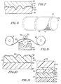
- the glass substrate 26 shown in Figure 3 has the surface 27 coated with a release film 31 formed of a suitable material such as silicone oil to a thickness of approximately 0.1 micron or less.
- a photoresist layer 32 is deposited over the release film 31 in a suitable manner such as by supplying a liquid negative photoresist in the form of a photopolymer as for example, an Eastman Kodak photoresist and spinning it onto the surface of the release film 31 and drying the same in a conventional manner.
- the photoresist layer 32 After the photoresist layer 32 has dried or cured, the photoresist layer 32 is stripped from the surface 27 of the etched glass substrate 26 to provide a negative replica of the surface 27 of the etched glass 26 as shown in Figure 4.
- the photoresist master 32 may be created using e-beam lithography techniques utilizing the computer generated pattern.
- the photoresist layer 32 has a surface 33 which is a negative of the surface 27 which is desired to replicate. This surface is utilized to provide a positive replica master shim 36 having a surface 37 which creates a positive replication of the etched surface 27 of the glass substrate 26.
- a negative replica master shim can be provided which creates a negative replication of an etched surface.
- This shim 36 can be formed of a suitable material such as gold in a conventional electroless plating method to provide a gold master shim 36 having a surface 37 which is a positive replication of the surface 27 of the glass substrate 26.
- the photoresist layer 32 can be dissolved or washed away in a conventional manner so that there remains a gold film master shim 36 having the surface 37 as shown in Figure 6.
- the shim 36 can be of a suitable size as for example 1/2" by 1/2" square.
- a plurality of tiling shims 41 are then formed from the gold film master shim 36 to provide surfaces 42 on the shims 41 which are the negatives of the surface 27 of the glass substrate 26 and a surface 43.
- a release layer 44 formed of a suitable material such as a silicone oil or sodium chloride is placed on the surface 37 of the master shim 36 and thereafter a metal such as nickel is electroplated in an electroless plating technique onto the surface 37 to a suitable thickness as for example 10 microns. After the plating has been finished, the release layer 44 is dissolved so there remains the surface 42 which carries the second negative image of the etched surface 27 of the glass 26.
- the nickel shims can have suitable dimensions as for example the same 1/2" by 1/2" dimensions as the gold film master shim 36.
- the roller 46 can be formed of a suitable material such as stainless steel or aluminum. For example, utilizing a cylindrical surface having a diameter of 6" inches and a width of 36" and utilizing tiling shims 1/2" square, in excess of 2000 shims would be required to cover that surface.
- the nickel tiling shims would then be taken and have their surfaces 43 secured to the cylindrical surface 47 by adhering the surfaces 43 to the cylindrical surface 47 by a suitable means such as an adhesive (not shown) and placing the shims 46 side by side and end to end in a matte to provide a surface pattern corresponding to the surfaces 42 of the shims 41 facing outwardly and radially from the cylindrical surface 47 to provide a cylindrical embossing surface.
- the roller 46 can be used to directly emboss the pattern carried thereby onto the hard coated surface of a flexible substrate as for example the PET substrate carrying an acrylic hard coat. This can be accomplished by use of a suitable temperature and pressure as for example a temperature of 150°C and 80 pounds per square inch and running the substrate between the embossing cylinder and a smooth steel roller.
- the embossing roller or cylinder 46 can be utilized in an apparatus and system such as shown in Figure 9.
- the PET substrate 22 is carried on a supply reel 51 and travels between the embossing roller 46 and a glass roller 52 that has an ultraviolet light source 53 therein and is then taken up by a take up reel 54.
- the embossing roller 46 travels through a liquid in the form of an ultraviolet (UV) curable polymer bath 56 disposed within an open top tank 57.
- the curable polymer bath can be in the form of a UV curable acrylic polymer or an epoxy based polymer within a fast cure heat curable polymer system using an IR heat source.
- the embossing roller 46 picks up a thin layer of the ultraviolet curable polymer from the bath 56 and engages the other under side or lower surface 24 of the substrate 22 and squeezes the polymer from the bath into the pattern on the shims 41 carried by the embossing roller 46.
- a doctor blade 64 can be utilized to remove excess polymer from the embossing roller before the polymer arrives at the underside of the flexible substrate 22.
- the polymer in contact with the embossing roller 46 is cured by the UV light source 53 to provide a cast embossed film 61 adherent to the surface 24 of the substrate 22 and to cause the layer 61 to be formed of a suitable thickness as for example 2 microns and to separate from the embossing roller 46 as it continues to rotate.
- the cured polymer layer 61 then travels with the substrate 22 as an embossed substrate 21 onto the take-up reel 54. After completion of the operation shown in Figure 9, the take up reel 54 can be shipped to the customer where it can be utilized for making photoreceptor devices of the type hereinbefore described.
- the layer 61 provides an embossed surface 62 for the substrate 22 which is a positive or negative of the pattern provided by the etched surface 27 of the glass substrate 26 which it was desired to replicate.
- the surface 62 can be provided with a vacuum deposited ground plane 66 formed of a suitable material such as metal.
- a vacuum deposited ground plane 66 formed of a suitable material such as metal. This can be readily accomplished by passing the embossed substrate 21 carried by the take up reel 54 and advancing the same through a conventional vacuum chamber to metalize the surface 62 to provide a conformal coating serving as the ground plane by evaporating aluminum or other suitable metallic material inside the vacuum chamber.
- the embossed and metalized substrate can then be wound up on another take-up reel (not shown) and thereafter shipped to the customer for fabrication into photoreceptor devices.
- the embossed substrate 21 with or without the vacuum deposited ground plane 66 can be utilized for making photoreceptor devices as for example the device 69 shown in Figure 11.
- the embossed surface 62 was provided with the ground plane 66 as hereinbefore described followed by a series of organic coatings of a type well known to those skilled in the art.
- a subbing adhesion layer/charge blocking layer 71 overlying the ground plane 66.
- a charge generation layer 72 and a charge transport layer 73 to provide the finished product 69.
- the PET substrate 22 can have a suitable thickness as for example 75 microns.
- the cast embossed film or layer can have a suitable thickness as for example 2 microns.
- the ground plane can have a thickness of less than 0.1 microns.
- the subbing adhesion layer or /charge blocking layer 71 can have a thickness greater than 1 micron and the charge generation layer 72 can have a thickness ranging from 0.1 to 1 micron and the charge transport layer 73 can have a thickness of 20 microns.
- the photoreceptor device 69 is provided with an embossed surface 62 which overlies the substrate 22 and provides a light diffusing capability for the photoreceptor device 69 which minimizes or eliminates optical interference (moire) effects such as color or wood graining in the image emitted through the charge transport layer 73 even though thin planar organic layers may be utilized which overlie the ground plane 66.
- embossed surface 62 which overlies the substrate 22 and provides a light diffusing capability for the photoreceptor device 69 which minimizes or eliminates optical interference (moire) effects such as color or wood graining in the image emitted through the charge transport layer 73 even though thin planar organic layers may be utilized which overlie the ground plane 66.
- the embossed surface 62 as described in connection with the surface 27 of the glass 26 has a topography in which the ridges and valleys provided are in a randomized non-periodic pattern and in which the ridges and valleys are more widely spaced from each other than the vertical distance between the peaks and the valleys to provide a microscale topography which diffuses light and does not have any coherent interference effects.
- the average roughness R a should be less than 300 nanometers and greater than 100 nanometers.
- the photoreceptor device can be utilized with laser printers typically using infrared laser diodes for a light source having a wave length ranging from 780 to 950 nanometers.
- the present invention is particularly applicable to IR laser copiers and printers.
- the same type of photoreceptor device as described in the present invention can be utilized in white light copying machines.
Landscapes
- Engineering & Computer Science (AREA)
- Mechanical Engineering (AREA)
- Physics & Mathematics (AREA)
- General Physics & Mathematics (AREA)
- Shaping Of Tube Ends By Bending Or Straightening (AREA)
- Photoreceptors In Electrophotography (AREA)
- Laminated Bodies (AREA)
- Credit Cards Or The Like (AREA)
- Silver Salt Photography Or Processing Solution Therefor (AREA)
- Paints Or Removers (AREA)
- Inks, Pencil-Leads, Or Crayons (AREA)
- Optical Elements Other Than Lenses (AREA)
Claims (22)
- Geprägtes Substrat, das ein Substrat aus einem Kunststoff umfasst und das eine Oberfläche und eine geprägte Oberfläche, die durch die Oberfläche des Substrates getragen wird, aufweist, wobei die geprägte Oberfläche ein Muster mit einer durchschnittlichen Rautiefe zwischen 100 Nanometer und 300 Nanometer aufweist, wobei die Rautiefe im Wesentlichen einheitlich über die Oberfläche hinweg verteilt ist, wobei das Muster Erhöhungen und Vertiefungen aufweist, wobei das Verhältnis des Abstandes zwischen benachbarten Erhöhungen und/oder benachbarten Vertiefungen zu der Tiefe zwischen den Erhöhungen und den Vertiefungen größer als 20 ist und wobei die Erhöhungen und die Vertiefungen zufällig, ohne Periodizität, angeordnet sind, um eine Diffusion von darauf auftreffendem Licht zu verursachen, sodass störende Einflüsse minimiert oder eliminiert werden, wenn die geprägte Oberfläche dem Licht ausgesetzt ist.
- Substrat nach Anspruch 1, wobei die geprägte Oberfläche die Oberfläche des Substrates ist.
- Substrat nach Anspruch 2, das weiter eine harte Beschichtung auf der Oberfläche des Substrates umfasst.
- Substrat nach Anspruch 3, wobei das Substrat PET ist und wobei die harte Beschichtung ein Acrylharzderivat ist.
- Substrat nach Anspruch 1, das weiterhin eine separate Schicht aus Kunststoff umfasst, die eine erste und eine zweite Oberfläche aufweist, wobei die erste Oberfläche der Schicht an die Oberfläche des Substrates adhäriert ist und wobei die geprägte Oberfläche in der zweiten Oberfläche der Schicht gebildet ist.
- Substrat nach Anspruch 5, wobei die Schicht aus einem ultraviolettaushärtbaren Polymer gebildet ist.
- Substrat nach Anspruch 6, wobei das Substrat aus PET gebildet ist.
- Substrat nach Anspruch 7, das weiter ein im Vakuum abgeschiedenes Metall umfasst, das auf der geprägten Oberfläche gebildet wurde.
- Substrat nach Anspruch 1, das die Struktur eines Abstandhalters aufweist.
- Fotorezeptorvorrichtung, umfassend ein Kunststoffsubstrat, das eine geprägte Oberfläche trägt, wobei die geprägte Oberfläche ein Muster mit einer durchschnittlichen Rautiefe zwischen 100 Nanometer und 300 Nanometer aufweist, wobei die Rautiefe im Wesentlichen einheitlich über die geprägte Oberfläche hinweg verteilt ist, wobei das Muster Erhöhungen und Vertiefungen aufweist, wobei das Verhältnis des Abstandes zwischen benachbarten Erhöhungen und/oder benachbarten Vertiefungen zu der Tiefe zwischen dem oberen Ende der Erhöhungen und dem unteren Ende der Vertiefungen größer als 20 ist, wobei die Erhöhungen und die Vertiefungen zufällig, ohne Periodizität, innerhalb des Musters angeordnet sind, eine an die geprägte Oberfläche adhärierte Grundflächenschicht, eine an die Grundflächenschicht adhärierte Ladungstrennschicht, eine an die Ladungstrennschicht adhärierte Ladungserzeugungsschicht und eine an die Ladungserzeugungsschicht adhärierte Ladungstransportschicht, wobei die geprägte Oberfläche dazu dient, eine Diffusion von darauf auftreffendem Licht zu verursachen und dazu dient, störende optische Einflüsse zu minimieren oder zu eliminieren, wenn die Fotorezeptorvorrichtung dem Licht ausgesetzt ist.
- Vorrichtung nach Anspruch 10, wobei das Substrat mit einer Oberfläche bereitgestellt ist, die aus einer harten Acrylharzbeschichtung gebildet ist und wobei das Muster in diese harte Acrylharzbeschichtung geprägt ist.
- Vorrichtung nach Anspruch 10, wobei die geprägte Oberfläche in der Kunststoffschicht gebildet ist.
- Vorrichtung nach Anspruch 12, wobei die geprägte Oberfläche in die Schicht gegossen ist.
- Vorrichtung nach Anspruch 10, wobei das Substrat aus PET gebildet ist.
- Verfahren zur Bereitstellung eines Abstandhalters, wobei das Verfahren umfasst:Bereitstellen eines Abdrucks einer Oberfläche mit einer durchschnittlichen Rautiefe zwischen 100 Nanometer und 300 Nanometer, wobei die Rautiefe im Wesentlichen einheitlich über die Oberfläche verteilt ist und mit einem Muster, das Erhöhungen und Vertiefungen aufweist, wobei das Verhältnis des horizontalen Abstandes zwischen benachbarten Erhöhungen und/oder benachbarten Vertiefungen zu dem vertikalen Abstand zwischen den oberen Enden der Erhöhungen und den unteren Enden der Vertiefungen größer als 20 ist, wobei die Erhöhungen und Vertiefungen zufällig, ohne Periodizität, in dem Muster angeordnet sind; undBilden einer geprägten Oberfläche auf der Oberfläche des Abstandhalters, die der nachgebildeten Oberfläche entspricht.
- Verfahren nach Anspruch 15, wobei der nachgebildete Abstandhalter verwendet wird, um direkt die Oberfläche des Substrates zu prägen.
- Verfahren nach Anspruch 15, wobei der nachgebildete Abstandhalter verwendet wird, um die Oberfläche einer separaten Kunststoffschicht, die an die Oberfläche des Substrates adhäriert ist, zu prägen.
- Verfahren nach Anspruch 15, wobei das Bild einer Oberfläche erzeugt wird durch Bilden einer negativen Oberflächentopographie des Musters einer gewünschten Oberfläche, Bilden einer positiven Oberflächentopographie durch Nachbilden der negativen Oberflächentopographie, Bilden einer weiteren negativen Oberflächentopographie durch Nachbilden der positiven Oberflächentopographie und abschließend Übertragen der negativen Oberflächentopographie in ein Kunststoffsubstrat, das geprägt ist und Erzeugen eines positiven Abdrucks der gewünschten Oberfläche in dem Kunststoffsubstrat.
- Verfahren nach Anspruch 18, wobei die positive Oberflächentopographie in einer Metallschicht gebildet wird und wobei eine weitere negative Oberflächentopographie in einer zusätzlichen Metallschicht gebildet wird.
- Verfahren nach Anspruch 19, wobei die negative Oberflächentopographie zusammen mit einer Prägewalze, die eine zylindrische Oberfläche aufweist, in einer Vielzahl von Abstandhaltern gebildet wird und wobei die Vielzahl von Abstandhaltern in einem Abdeckungsformat auf der zylindrischen Oberfläche der Prägewalze befestigt wird, wobei die Prägewalze durch ein ultraviolettaushärtbares Polymerbad wandert und wobei das ultraviolettaushärtbare Polymer auf eine Seite des Substrats übertragen wird, während das ultraviolettaushärtbare Polymer mit einem ultraviolettaushärtenden Licht behandelt wird, damit das ultraviolette Polymer aushärtet und fest wird und um es von der Prägewalze auf das Substrat zu übertragen, sodass das Substrat mit einer geprägten Oberfläche, die das Bild der gewünschten Oberfläche trägt, bereitgestellt wird.
- Verfahren nach Anspruch 20 zusammen mit dem Schritt des Auftragens einer im Vakuum abgeschiedenen Grundflächenschicht auf die geprägte Oberfläche.
- Verfahren nach Anspruch 21 zusammen mit den Schritten des Ablagerns einer Vielzahl von organischen Schichten, die die Grundflächenschicht überlagern.
Applications Claiming Priority (3)
| Application Number | Priority Date | Filing Date | Title |
|---|---|---|---|
| US555530 | 1995-11-09 | ||
| US08/555,530 US5670240A (en) | 1995-11-09 | 1995-11-09 | Embossed substrate and photoreceptor device incorporating the same and method |
| PCT/US1996/018096 WO1997017193A1 (en) | 1995-11-09 | 1996-11-07 | Embossed substrate and photoreceptor device incorporating the same and method |
Publications (3)
| Publication Number | Publication Date |
|---|---|
| EP0802854A1 EP0802854A1 (de) | 1997-10-29 |
| EP0802854A4 EP0802854A4 (de) | 1998-01-21 |
| EP0802854B1 true EP0802854B1 (de) | 2002-01-30 |
Family
ID=24217614
Family Applications (1)
| Application Number | Title | Priority Date | Filing Date |
|---|---|---|---|
| EP96940776A Expired - Lifetime EP0802854B1 (de) | 1995-11-09 | 1996-11-07 | Geprägtes substrat und photoreceptor-vorrichtung die dieses beinhaltet und verfahren |
Country Status (10)
| Country | Link |
|---|---|
| US (3) | US5670240A (de) |
| EP (1) | EP0802854B1 (de) |
| JP (1) | JPH10512513A (de) |
| CN (1) | CN1086630C (de) |
| AU (1) | AU1075297A (de) |
| CA (1) | CA2209852C (de) |
| DE (1) | DE69618929T2 (de) |
| DK (1) | DK0802854T3 (de) |
| TW (1) | TW337003B (de) |
| WO (1) | WO1997017193A1 (de) |
Families Citing this family (37)
| Publication number | Priority date | Publication date | Assignee | Title |
|---|---|---|---|---|
| US5885672A (en) * | 1989-04-26 | 1999-03-23 | Flex Products, Inc. | Coated barrier film and packaging utilizing the same and method |
| US5670240A (en) * | 1995-11-09 | 1997-09-23 | Flex Products, Inc. | Embossed substrate and photoreceptor device incorporating the same and method |
| SG71168A1 (en) * | 1997-11-14 | 2000-03-21 | Gen Electric | Method for producing textured thermoplastic film |
| US6855415B2 (en) | 1997-11-14 | 2005-02-15 | General Electric Company | Coated thermoplastic film substrate |
| JP3808212B2 (ja) * | 1998-07-31 | 2006-08-09 | 日立化成工業株式会社 | 転写フィルム及び拡散反射板の製造法 |
| US6761958B2 (en) | 2001-09-06 | 2004-07-13 | Toray Plastics (America), Inc. | Embossable thermoplastic polyester film and method for producing the film |
| US6737170B2 (en) | 2001-09-06 | 2004-05-18 | Toray Plastics (America), Inc. | Coated film with exceptional embossing characteristics and method for producing it |
| DE10158347A1 (de) * | 2001-11-28 | 2003-06-12 | Tesa Ag | Verfahren zur Erzeugung von nano- und mikrostrukturierten Polymerfolien |
| US6979419B2 (en) * | 2002-03-07 | 2005-12-27 | Robert Cameron | Method of manufacturing a print pad having a surface textured for printing on a highly polished surface such as a contact lens or a contact lens mold |
| US7010212B2 (en) * | 2002-05-28 | 2006-03-07 | 3M Innovative Properties Company | Multifunctional optical assembly |
| JP4213989B2 (ja) * | 2003-05-08 | 2009-01-28 | 富士フイルム株式会社 | 防眩性フィルムの製造方法 |
| US20040265193A1 (en) * | 2003-06-03 | 2004-12-30 | Ron Panice | In-line, automated, duct-washing apparatus |
| US7063820B2 (en) * | 2003-06-16 | 2006-06-20 | University Of Florida Research Foundation, Inc. | Photoelectrochemical air disinfection |
| US20050130335A1 (en) * | 2003-12-15 | 2005-06-16 | Eiichi Ito | Method of manufacturing master of optical information recording medium, method of manufacturing stamper of optical information recording medium, master and stamper of an optical information recording medium, and optical information recording medium |
| US7470386B2 (en) * | 2004-04-26 | 2008-12-30 | Sipix Imaging, Inc. | Roll-to-roll embossing tools and processes |
| US20060154050A1 (en) * | 2004-05-18 | 2006-07-13 | Toray Plastics (America), Inc., A Corporation Of Rhode Island | Holographic transfer thermoplastic sheet |
| GB0605360D0 (en) | 2006-03-16 | 2006-04-26 | Dupont Teijin Films Us Ltd | Method of manufacture |
| ES2435530T3 (es) * | 2009-05-14 | 2013-12-20 | Flooring Technologies Ltd. | Procedimiento para la estructuración de un elemento de revestimiento del suelo |
| JP5227909B2 (ja) * | 2009-07-13 | 2013-07-03 | 財団法人神奈川科学技術アカデミー | スタンパおよびそれを用いた反射防止膜の製造方法 |
| CN102128782A (zh) * | 2010-12-03 | 2011-07-20 | 南京航空航天大学 | 基于实体模型的腐蚀损伤测量方法及测量装置 |
| FR2971060B1 (fr) * | 2011-01-31 | 2013-08-09 | Saint Gobain | Element transparent a reflexion diffuse |
| US8795778B2 (en) | 2011-10-19 | 2014-08-05 | Unipixel Displays, Inc. | Photo-patterning using a translucent cylindrical master to form microscopic conductive lines on a flexible substrate |
| EP3955042B1 (de) | 2013-08-26 | 2024-08-21 | S.D. Sight Diagnostics Ltd. | Digitale mikroskopiesysteme, verfahren und computerprogrammprodukte |
| CN104582352B (zh) * | 2013-10-25 | 2017-06-13 | 富鼎电子科技(嘉善)有限公司 | 电子装置外壳及其采用的立体图案结构 |
| JP6217679B2 (ja) | 2015-03-25 | 2017-10-25 | コニカミノルタ株式会社 | 電気機器用オプション装置 |
| CN104966789A (zh) * | 2015-06-30 | 2015-10-07 | 深圳市华星光电技术有限公司 | 一种电荷连接层及其制造方法、叠层oled器件 |
| CN108474934B (zh) | 2015-09-17 | 2022-01-18 | 思迪赛特诊断有限公司 | 用于检测身体样本中实体的方法和设备 |
| DE102015120535A1 (de) | 2015-11-26 | 2017-06-01 | Leibniz-Institut für Oberflächenmodifizierung e.V. | Vorrichtung und Verfahren zur Herstellung einer beidseitig mikrostrukturierten Folie |
| WO2017168411A1 (en) | 2016-03-30 | 2017-10-05 | S.D. Sight Diagnostics Ltd | Image processing device for identifying blood parasites |
| EP3455610B1 (de) * | 2016-05-11 | 2023-01-04 | S.D. Sight Diagnostics Ltd. | Probenträger für optische messungen |
| US11099175B2 (en) | 2016-05-11 | 2021-08-24 | S.D. Sight Diagnostics Ltd. | Performing optical measurements on a sample |
| CN111788471B (zh) | 2017-11-14 | 2023-12-12 | 思迪赛特诊断有限公司 | 用于光学测量的样品载体 |
| AT520942B1 (de) * | 2018-03-15 | 2019-09-15 | Werner Faerber | Verfahren zur Herstellung einer Lichtlenkfolie und damit hergestellte Folie |
| CA3155820A1 (en) | 2019-10-22 | 2021-04-29 | S.D. Sight Diagnostics Ltd | Accounting for errors in optical measurements |
| CN114787685B (zh) | 2019-12-12 | 2025-10-17 | 思迪赛特诊断有限公司 | 人工生成彩色血液涂片图像 |
| MX2022007123A (es) | 2019-12-12 | 2022-07-11 | S D Sight Diagnostics Ltd | Analisis de un analito dispuesto dentro de un medio. |
| CN114787625B (zh) | 2019-12-12 | 2026-01-13 | 思迪赛特诊断有限公司 | 检测血液样品中的血小板 |
Family Cites Families (20)
| Publication number | Priority date | Publication date | Assignee | Title |
|---|---|---|---|---|
| GB660279A (en) * | 1948-09-14 | 1951-11-07 | Dunlop Rubber Co | Improvements in or relating to the production of thermoplastic materials having grained or patterned surfaces |
| US3235631A (en) * | 1962-08-23 | 1966-02-15 | Ind Biology Lab Inc | Polarization process |
| US4114983A (en) * | 1977-02-18 | 1978-09-19 | Minnesota Mining And Manufacturing Company | Polymeric optical element having antireflecting surface |
| US4588667A (en) * | 1984-05-15 | 1986-05-13 | Xerox Corporation | Electrophotographic imaging member and process comprising sputtering titanium on substrate |
| JPS6161835A (ja) * | 1984-08-31 | 1986-03-29 | Sekisui Chem Co Ltd | エンボス加工された熱可塑性樹脂シ−トの製造方法 |
| US4711833A (en) * | 1986-03-24 | 1987-12-08 | Xerox Corporation | Powder coating process for seamless substrates |
| US4840757A (en) * | 1987-05-19 | 1989-06-20 | S. D. Warren Company | Replicating process for interference patterns |
| US5164227A (en) * | 1987-06-19 | 1992-11-17 | Van Leer Metallized Products (Usa) Limited | Method for embossing a coated sheet with a diffraction or holographic pattern |
| US5155604A (en) * | 1987-10-26 | 1992-10-13 | Van Leer Metallized Products (Usa) Limited | Coated paper sheet embossed with a diffraction or holographic pattern |
| CN1013748B (zh) * | 1988-01-28 | 1991-09-04 | 安徽工学院 | 聚晶金刚石的机械电脉冲成型加工方法 |
| US4954297A (en) * | 1988-12-05 | 1990-09-04 | The Mead Corporation | Method and apapratus for forming a matte finish on resin-coated webs or sheets |
| EP0462439A1 (de) * | 1990-06-21 | 1991-12-27 | Xerox Corporation | Unterdrückung von Interferenzeffekten in lichtempfindlichen Bildherstellungselementen |
| JPH0641108B2 (ja) * | 1991-03-28 | 1994-06-01 | 富士ゼロックス株式会社 | 湿式ホーニング用研磨材懸濁液及びそれを用いた表面処理方法 |
| JPH06126915A (ja) * | 1992-10-15 | 1994-05-10 | Mitsubishi Petrochem Co Ltd | 熱圧着プリントラミネート用フィルム |
| US5302485A (en) * | 1993-01-04 | 1994-04-12 | Xerox Corporation | Method to suppress plywood in a photosensitive member |
| US5425977A (en) * | 1993-08-16 | 1995-06-20 | Monsanto Company | Rough-surfaced interlayer |
| US5483890A (en) * | 1995-03-15 | 1996-01-16 | Gencorp Inc. | Direct applied embossing casting methods |
| US5635324A (en) * | 1995-03-20 | 1997-06-03 | Xerox Corporation | Multilayered photoreceptor using a roughened substrate and method for fabricating same |
| US5706106A (en) * | 1995-05-25 | 1998-01-06 | Pennsylvania Pulp And Paper Co. | Graphic works involving holography |
| US5670240A (en) * | 1995-11-09 | 1997-09-23 | Flex Products, Inc. | Embossed substrate and photoreceptor device incorporating the same and method |
-
1995
- 1995-11-09 US US08/555,530 patent/US5670240A/en not_active Expired - Lifetime
-
1996
- 1996-11-07 EP EP96940776A patent/EP0802854B1/de not_active Expired - Lifetime
- 1996-11-07 WO PCT/US1996/018096 patent/WO1997017193A1/en not_active Ceased
- 1996-11-07 CN CN96191906A patent/CN1086630C/zh not_active Expired - Fee Related
- 1996-11-07 DE DE69618929T patent/DE69618929T2/de not_active Expired - Fee Related
- 1996-11-07 CA CA002209852A patent/CA2209852C/en not_active Expired - Fee Related
- 1996-11-07 JP JP9518386A patent/JPH10512513A/ja active Pending
- 1996-11-07 DK DK96940776T patent/DK0802854T3/da active
- 1996-11-07 AU AU10752/97A patent/AU1075297A/en not_active Abandoned
- 1996-11-09 TW TW085113709A patent/TW337003B/zh not_active IP Right Cessation
-
1997
- 1997-06-04 US US08/868,986 patent/US5789125A/en not_active Expired - Fee Related
- 1997-06-04 US US08/868,904 patent/US5993702A/en not_active Expired - Lifetime
Also Published As
| Publication number | Publication date |
|---|---|
| TW337003B (en) | 1998-07-21 |
| EP0802854A1 (de) | 1997-10-29 |
| US5670240A (en) | 1997-09-23 |
| CA2209852A1 (en) | 1997-05-15 |
| JPH10512513A (ja) | 1998-12-02 |
| EP0802854A4 (de) | 1998-01-21 |
| US5789125A (en) | 1998-08-04 |
| CN1086630C (zh) | 2002-06-26 |
| AU1075297A (en) | 1997-05-29 |
| DE69618929D1 (de) | 2002-03-14 |
| CN1173843A (zh) | 1998-02-18 |
| CA2209852C (en) | 2001-01-09 |
| DK0802854T3 (da) | 2002-05-21 |
| WO1997017193A1 (en) | 1997-05-15 |
| DE69618929T2 (de) | 2002-06-27 |
| US5993702A (en) | 1999-11-30 |
Similar Documents
| Publication | Publication Date | Title |
|---|---|---|
| EP0802854B1 (de) | Geprägtes substrat und photoreceptor-vorrichtung die dieses beinhaltet und verfahren | |
| US5948199A (en) | Surface relief holograms and holographic hot-stamping foils, and method of fabricating same | |
| US6358442B1 (en) | Animated light diffracting, prismatic refracting, and/or holographic surface papers, board and other substrates and low-cost pattern transfer method of manufacturing the same | |
| US4840757A (en) | Replicating process for interference patterns | |
| US4758296A (en) | Method of fabricating surface relief holograms | |
| KR101369816B1 (ko) | 회절 격자를 사용한 보안 인쇄 | |
| JP3211828B2 (ja) | ホログラムの製造方法および製造装置 | |
| US8241479B2 (en) | Imaging of deep structures of reliefs for shallow relief embossing | |
| JP2001511725A (ja) | 複製及びその材料の形成方法 | |
| US5238516A (en) | Method for embossing holograms | |
| JPS60169887A (ja) | ホログラム画像再生用転写シ−ト及び物品表面にホログラム画像を再生する方法 | |
| US20030221769A1 (en) | Transfer casting of holographic images | |
| JP4170747B2 (ja) | 光回折層を有する転写箔 | |
| JP3810473B2 (ja) | ホログラムが形成された軟質ポリ塩化ビニル積層体およびその製造方法 | |
| JPH11291677A (ja) | レリーフovdパターン画像形成方法 | |
| JP2000010482A (ja) | 光回折構造、光回折構造転写シート及び光回折構造付きカード | |
| JP2017032986A (ja) | ホログラム転写箔およびホログラム印刷物 | |
| JP2005119259A (ja) | 高光反射性の透明積層フィルム及びその製造方法、並びに液晶表示装置 | |
| WO2023170376A1 (en) | Security document substrate and method of manufacture thereof | |
| JPWO2023104653A5 (de) | ||
| JPH09234824A (ja) | アルミニウム薄膜積層紙およびアルミニウム薄膜積層紙の製造方法 | |
| JP2002283774A (ja) | 後加工適性および耐久性に優れた光回折構造転写シートおよびカード |
Legal Events
| Date | Code | Title | Description |
|---|---|---|---|
| PUAI | Public reference made under article 153(3) epc to a published international application that has entered the european phase |
Free format text: ORIGINAL CODE: 0009012 |
|
| 17P | Request for examination filed |
Effective date: 19970717 |
|
| AK | Designated contracting states |
Kind code of ref document: A1 Designated state(s): BE DE DK FR GB IT SE |
|
| A4 | Supplementary search report drawn up and despatched |
Effective date: 19971203 |
|
| AK | Designated contracting states |
Kind code of ref document: A4 Designated state(s): BE DE DK FR GB IT SE |
|
| 17Q | First examination report despatched |
Effective date: 19991208 |
|
| GRAG | Despatch of communication of intention to grant |
Free format text: ORIGINAL CODE: EPIDOS AGRA |
|
| GRAG | Despatch of communication of intention to grant |
Free format text: ORIGINAL CODE: EPIDOS AGRA |
|
| GRAG | Despatch of communication of intention to grant |
Free format text: ORIGINAL CODE: EPIDOS AGRA |
|
| GRAH | Despatch of communication of intention to grant a patent |
Free format text: ORIGINAL CODE: EPIDOS IGRA |
|
| GRAH | Despatch of communication of intention to grant a patent |
Free format text: ORIGINAL CODE: EPIDOS IGRA |
|
| GRAA | (expected) grant |
Free format text: ORIGINAL CODE: 0009210 |
|
| REG | Reference to a national code |
Ref country code: GB Ref legal event code: IF02 |
|
| AK | Designated contracting states |
Kind code of ref document: B1 Designated state(s): BE DE DK FR GB IT SE |
|
| REF | Corresponds to: |
Ref document number: 69618929 Country of ref document: DE Date of ref document: 20020314 |
|
| ET | Fr: translation filed | ||
| REG | Reference to a national code |
Ref country code: DK Ref legal event code: T3 |
|
| PLBE | No opposition filed within time limit |
Free format text: ORIGINAL CODE: 0009261 |
|
| STAA | Information on the status of an ep patent application or granted ep patent |
Free format text: STATUS: NO OPPOSITION FILED WITHIN TIME LIMIT |
|
| 26N | No opposition filed | ||
| PGFP | Annual fee paid to national office [announced via postgrant information from national office to epo] |
Ref country code: GB Payment date: 20031029 Year of fee payment: 8 |
|
| PGFP | Annual fee paid to national office [announced via postgrant information from national office to epo] |
Ref country code: FR Payment date: 20031119 Year of fee payment: 8 |
|
| PGFP | Annual fee paid to national office [announced via postgrant information from national office to epo] |
Ref country code: SE Payment date: 20031121 Year of fee payment: 8 Ref country code: DK Payment date: 20031121 Year of fee payment: 8 |
|
| PGFP | Annual fee paid to national office [announced via postgrant information from national office to epo] |
Ref country code: DE Payment date: 20031231 Year of fee payment: 8 |
|
| PGFP | Annual fee paid to national office [announced via postgrant information from national office to epo] |
Ref country code: BE Payment date: 20040115 Year of fee payment: 8 |
|
| PG25 | Lapsed in a contracting state [announced via postgrant information from national office to epo] |
Ref country code: GB Free format text: LAPSE BECAUSE OF NON-PAYMENT OF DUE FEES Effective date: 20041107 |
|
| PG25 | Lapsed in a contracting state [announced via postgrant information from national office to epo] |
Ref country code: SE Free format text: LAPSE BECAUSE OF NON-PAYMENT OF DUE FEES Effective date: 20041108 |
|
| PG25 | Lapsed in a contracting state [announced via postgrant information from national office to epo] |
Ref country code: DK Free format text: LAPSE BECAUSE OF NON-PAYMENT OF DUE FEES Effective date: 20041130 Ref country code: BE Free format text: LAPSE BECAUSE OF NON-PAYMENT OF DUE FEES Effective date: 20041130 |
|
| BERE | Be: lapsed |
Owner name: *FLEX PRODUCTS INC. Effective date: 20041130 |
|
| PG25 | Lapsed in a contracting state [announced via postgrant information from national office to epo] |
Ref country code: DE Free format text: LAPSE BECAUSE OF NON-PAYMENT OF DUE FEES Effective date: 20050601 |
|
| REG | Reference to a national code |
Ref country code: DK Ref legal event code: EBP |
|
| GBPC | Gb: european patent ceased through non-payment of renewal fee |
Effective date: 20041107 |
|
| EUG | Se: european patent has lapsed | ||
| PG25 | Lapsed in a contracting state [announced via postgrant information from national office to epo] |
Ref country code: FR Free format text: LAPSE BECAUSE OF NON-PAYMENT OF DUE FEES Effective date: 20050729 |
|
| REG | Reference to a national code |
Ref country code: FR Ref legal event code: ST |
|
| PG25 | Lapsed in a contracting state [announced via postgrant information from national office to epo] |
Ref country code: IT Free format text: LAPSE BECAUSE OF NON-PAYMENT OF DUE FEES Effective date: 20051107 |
|
| BERE | Be: lapsed |
Owner name: *FLEX PRODUCTS INC. Effective date: 20041130 |